
Semiconductor companies and semiconductor researchers are constantly looking for ways to make devices fail in the lab in order to prevent failures in the field. Countless hours are spent by failure analysis (FA) engineers trying to understand why a device failed and how it can be prevented in the future. This is vital as many devices are used in mission critical applications where “failure is not an option”, once said by Gene Kranz during the Apollo 13 mission in his role as lead flight director. But device failures do occur.
Microelectronics failure analysis is one of the main analytical methods applied to the diagnosis of problems occurring with devices, either in the fabrication phase or in the use of the package in the application. A semiconductor device electrical failure can be either functional or parametric. When a device is unable to perform its intended function, this failure is considered a functional failure. A parametric failure is when the device is unable to meet electrical specifications for a measurable characteristic. A typical parametric failure can be leakage current, which may not pertain to the device’s functionality. Thus, it is possible that a parametric failure may be present even if the device is still functional or able to perform its intended function.
How is Failure Analysis Performed?
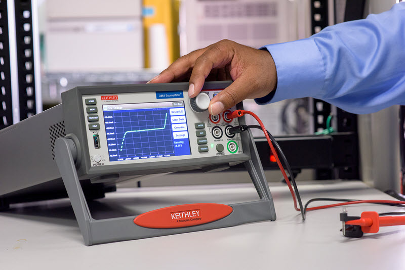
There are a number of failure analysis techniques for semiconductor devices. A quick, simple verification test involves using a source measure unit (SMU) where you can ramp up to an I-V curve anomaly and then use the SMU to seamlessly creep into the behavior, minimizing the risk of further damaging a (potentially) already damaged device.
Figure 1: Keithley’s I-V Tracer solution for failure verification.
Beyond I-V curve tracing, tests would fall into destructive and non-destructive testing. The objective is to determine the failure mechanism that led to the failure mode of the device. These failure mechanisms can come from potential fault lines in ICs from local heat dissipation, shorts between power or signal lines, oxide or junction breakdowns, latch-ups and much more. Unfortunately, destructive testing usually is necessary in a large portion of the analytical effort. Tasks such as decapsulation, scribing metal lines, and cross sectioning are some of the techniques used. Performed prematurely, however, these procedures can result in irreversible damage and a ruined analysis, ignoring the cost of the resources.
Nondestructive evaluation of failures has historically been a visual process, using tools like transmission electron microscopy and other x-ray inspections systems. These tools come at a very large price tag. Another technique that is cost effective is Lock-in Thermography (LiT). LiT addresses a number of challenges that customers have:
- Don’t want to destroy valuable devices under test (DUT).
- Need an easy way to periodically modulate the amplitude of the power dissipated in the DUT.
- Isolate problem sites or hot spots in packaged devices faster, reducing costs and getting to answers faster.

Figure 2: Lock-in Thermography can quickly identify hot spots in packaged semiconductor devices. Amplitude image (a), phase image (b), ε-corrected 0° image (c; 0°/-90° image from the region indicated in b), and power distribution (d), numerically deconvoluted from (c), of a hall sensor circuit2.
Why Lock-in Thermography?
Lock-in thermography is an active thermography technique used to analyze microelectronic devices or more general samples of materials in order to detect defects, damages, or characterize potential fabrication issues. LiT allows the contactless measurement of surface temperatures using an infrared thermal imaging camera. The “lock-in” part of the name comes from the requirement to sync the camera’s acquisition rate with the excitation of the circuit.
LiT consists of applying a periodic thermal excitation to a device under test in the form of a pulsed electrical signal, then monitoring the temperature variation with a thermal camera that captures multiple fast acquisitions and computes these with a post processing algorithm. For semiconductor package devices, this enables the failure analysis engineer to map the surface of the package and quickly identify localized hotspots with increased resolution and temperature distribution on the surface of the package.
How Tektronix/ Keithley can help to build an effective solution for Lock-in Thermography
A typical lock-in thermography system diagram would look like what is shown in Figure 3.
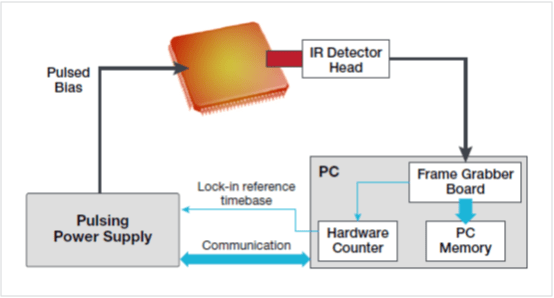
Figure 3: Block diagram for a typical Lock-in Thermography system.1
The above application could be addressed using a programmable arbitrary function generator, voltage pulse source, or a current source generator where appropriate, instead of the hardware counter and the pulsing power supply. Current pulsers, for example can output current pulses as high as 10 amps at 10 volts with very small pulse widths.
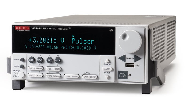
Reacting to the challenges we heard from FA engineers demanding an all-in-one instrument including a built-in programming function to coordinate the process and lock-in function with the thermal camera, Keithley – a Tektronix Company – developed the 2601B-PULSE System SourceMeter® 10 μs Pulser/SMU Instrument.

Figure 4: Keithley’s 2601B-PULSE System SourceMeter 10 μs Pulser/SMU Instrument.
The 2601B-PULSE is a high current/high speed pulser with measurement capability plus the full functionality of a traditional source measure unit. This new pulser offers leading 10 A current pulse output at 10 V with a pulse width minimum of 10 μs, with fast rise times as shown in Figure 6.
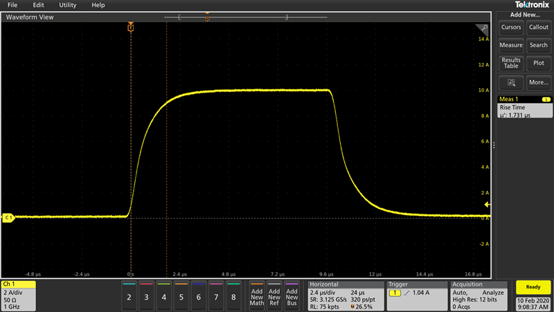
Figure 5: High fidelity 10A, 10ms pulse for application on a failed device.
The instrument also has a built-in timer function that eliminates the need for an external time reference. The internal timer has a free running 47-bit counter with 1 MHz clock input. The timer resolution is 1 μs and accuracy of ±100 ppm. Based upon the diagram in Figure 3, the 2601B-PULSE replaces the pulsing power supply and the hardware counter.
By using the 2601B-PULSE Pulser/SMU with a LAN/Ethernet enabled IR thermal camera, you can simplify the Lock-in Thermography configuration and allow the 2601B-PULSE to control the testing process while the PC runs the thermal analysis software as shown in Figure 6.
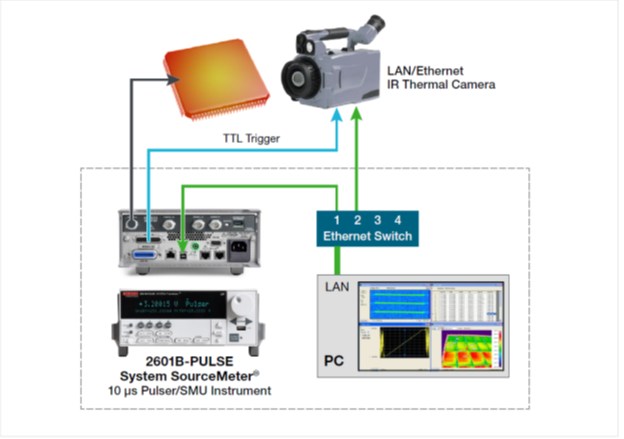
Figure 6: Example Lock-in Thermography System using the Keithley 2601B-PULSE.
Conclusion
Lock-in Thermography is just one technique for quickly identifying hotspots on the device to narrow down the location of a failure and continue the investigation to determine root cause. Instruments like the Keithley 2601B-PULSE and an LAN/Ethernet enabled IR thermal camera minimize the challenges of integrating advanced instrumentations to conduct the measurements. Lock-in Thermography reduces the need for destructive testing and helps to overcome the challenges that failure analysis presents at the package level, resulting in faster time to answer, more efficient use of the FA engineer’s time, and cost savings to the organization.
Download the full application note here.
References
1. APPLICATION OF LOCK-IN THERMOGRAPHY TO FAILURE ANALYSIS IN INTEGRATED CIRCUITS, FRAUNHOFER INSTITUTE FOR MECHANICS OF MATERIALS, MAX PLANCK INSTITUTE OF MICROSTRUCTURE PHYSICS, O. Breitenstein, Ch. Schmidt, F. Altmann, Halle, Germany, Microtherm 2011.
2. Thermal Failure Analysis by IR Lock-in Thermography, Microelectronics Failure Analysis Desk Reference, Breitenstein, Schmidt, Altamann, Karg, ASM International 2011.


