Kontaktaufnahme
Live-Chat mit Tektronix-Vertretern. Verfügbar von 9 bis 17 Uhr CET Geschäftstage.
Kontaktieren Sie uns telefonisch unter
Verfügbar von 9 bis 17 Uhr CET Geschäftstage.
Download
Laden Sie Handbücher, Datenblätter, Software und vieles mehr herunter:
Feedback
Ensuring Precision and Reliability in Electronic Innovation
The pace of semiconductor development is accelerating around the world thanks to near-daily breakthroughs in technology, market demand, and government policies. We depend on semiconductors in nearly every aspect of our lives for connectivity, professional tasks, and relaxation. Quantifying and guaranteeing the dependability of these electronics is crucial. Semiconductor testing is the broad process of ensuring reliability and performance across the material, device, and system levels of the semiconductor world.
Tektronix’s Comprehensive Suite of Semiconductor Test Solutions
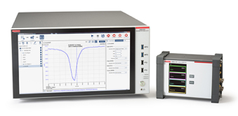
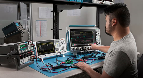
At Tektronix, we offer a range of semiconductor testing solutions tailored to the needs of designers, validation engineers and manufacturers. Keithley instruments deliver exceptional precision for validating device characteristics, from wafer to die to packaged device. EA Elektro-Automatik power supplies contribute high power for testing next-generation power semiconductors. And Tektronix oscilloscopes and signal sources help chip designers secure advances in high-speed data communications. With the global nature of the semiconductor industry, it's important to go with a vendor with global coverage, like Tektronix.
Materials Testing
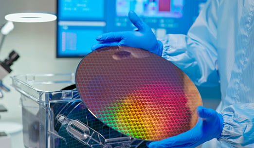
Materials testing in the power semiconductor industry involves examining materials like silicon carbide (SiC) and gallium nitride (GaN). This process, crucial for understanding their unique properties, plays a significant role in the manufacturing of power semiconductors. It contributes to the development of efficient and reliable electronic devices, shaping the future of the electronics industry. Learn more about the types of materials testing Tektronix offers below.
Device Testing
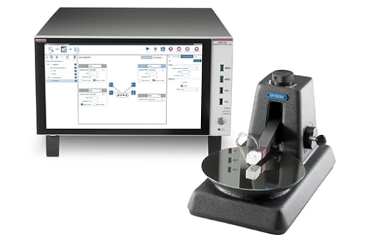
Device testing in the power semiconductor industry is a key process that evaluates the functionality, performance, and reliability of semiconductor devices. This testing ensures that these devices meet the required performance, reliability, and quality standards before they are incorporated into electronic products. It includes various techniques, one of which is I-V characterization, a fundamental method for understanding the relationship between current and voltage in power semiconductors. Learn more about the types of device testing Tektronix offers below.
System-Level Testing
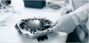
System-Level Testing in the power semiconductor industry is an all-encompassing process that checks the functionality and performance of semiconductor devices within a system context. This method of testing is becoming increasingly important as it can identify design issues that may not be detected at the wafer probe and package test stages. It enables the testing of millions of chips in parallel at high speeds, thereby increasing throughput while ensuring maximum test coverage. As semiconductor geometries shrink and more complexity is integrated into chips or packages, this approach to testing is becoming essential.
Resources Related to Semiconductor Testing
Stages of Semiconductor Testing
Semiconductor testing is a critical process in the manufacturing of semiconductor devices, ensuring that the final products meet the required specifications and are of high quality. The testing process is typically divided into several stages, including wafer testing, package testing, and final testing.

Wafer Testing
Wafer testing, also known as wafer sort or wafer probing, is the first stage of semiconductor testing. It is performed on the semiconductor wafer itself before it is cut into individual dies. The purpose of wafer testing is to identify any defects or failures at an early stage, thereby reducing waste and improving yield. During wafer testing, each die on the wafer is tested for functionality using a probe card that makes electrical contact with the die’s pads. Tektronix offers complete wafer testing services for mission-critical devices. Their capabilities include testing of 4", 6", 8", 12" wafers (100mm, 150mm, 200mm, 300mm) analog, digital, and mixed signal test.
Learn more about Tektronix wafer testing services
Case Study: Wafer Testing
Imagine you’re an engineer at a semiconductor manufacturing facility. You’ve just received a new batch of silicon wafers and it’s your job to test them. You start by loading the wafers into the wafer prober, a machine that can automatically position the wafer so that each die is under the probe card. The probe card comes down and makes contact with the pads on the die. The machine then runs a series of electrical tests to check the functionality of the die. If a die fails any of these tests, it’s marked as defective and will be discarded after the wafer is cut into individual dies.

Package Testing
After the wafer is cut into individual dies, the dies that passed the wafer testing are packaged. The packaged dies undergo another round of testing known as package testing or final testing. This stage of testing is more comprehensive and involves testing the packaged chips under various conditions to ensure they meet all the specified electrical, mechanical, and thermal performance criteria. Package testing can include tests for speed, power, and leakage current. Tektronix offers package testing services to ensure that your packaging will stand up to the rigors of distribution and storage.
Use Case: Package Testing
Now, imagine you’re in the package testing department. You receive the packaged dies from the wafer testing department. Your job is to ensure that these packaged chips are ready for the real world. You load the chips into the test sockets on a test board. The test equipment is programmed to run a series of tests that simulate the conditions the chips will face in their intended applications. These tests include checking the speed of the chip, its power consumption, and whether there are any leaks in the package. Any chips that fail these tests are discarded.
Final Testing
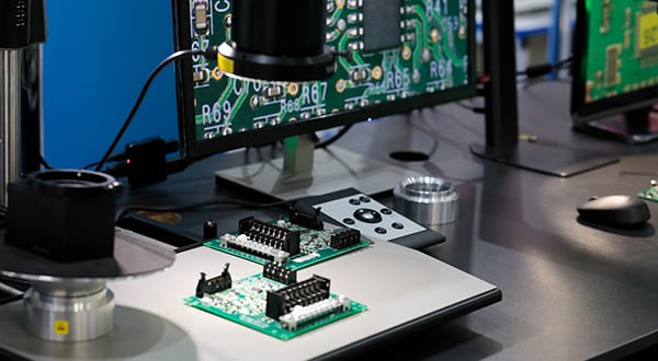
The final stage of semiconductor testing is the system-level testing or application testing. In this stage, the packaged chips are tested in a system similar to the one they will be used in. This ensures that the chips function correctly in real-world applications. Tektronix offers IC package test solutions to verify components and modules are operating at required performance levels.
Use Case: Final Testing
Finally, you’re in the system-level testing department. Here, the chips are no longer tested in isolation. Instead, they’re placed in a system that’s similar to the one they’ll be used in. This could be a mobile phone, a car’s electronic system, or a server in a data center. You monitor the system’s performance, making sure that the chip is working as expected in its intended environment. If the chip passes these tests, it’s ready to be shipped out to the customers.
In conclusion, semiconductor testing is a rigorous process that ensures the quality and reliability of semiconductor devices. It helps in identifying and eliminating defective chips, thereby ensuring that only high-quality devices make it to the market.
Advanced Semiconductor Testing Techniques
- DC Parametric Examination: This critical test assesses the semiconductor's behavior under various direct current (DC) conditions. It involves measuring parameters like leakage current, threshold voltage, and saturation current, which are vital for assessing device performance and stability.
- AC Parametric Examination: This test evaluates how the semiconductor responds to alternating current (AC) at different frequencies. It's essential for devices used in AC applications, ensuring they maintain performance across a range of operating conditions.
- Functional Examination: This comprehensive test verifies that the semiconductor performs its intended function correctly. It includes checking logic operations in transistors and ensuring diodes correctly regulate voltage.
- Burn-In Examination: This long-duration test exposes semiconductors to extreme conditions to accelerate aging. By doing this, manufacturers can identify early failures and improve overall reliability.
- Electrostatic Discharge (ESD) Examination: ESD testing is crucial for determining a semiconductor's vulnerability to sudden discharges of static electricity, which are common in everyday environments.
- Thermal Characteristic Examination: This test evaluates how well the semiconductor dissipates heat, an essential factor for preventing overheating and ensuring long-term reliability.
- Mechanical Property Examination: This test checks the semiconductor's physical resilience, ensuring it can withstand mechanical stresses like vibration and shock during operation and transportation.
- X-ray Analysis: Non-destructive and insightful, X-ray analysis reveals internal structures and possible hidden defects like cracks or misalignments in semiconductor layers.
- Scanning Electron Microscopy (SEM) Analysis: SEM provides high-resolution imaging of the semiconductor surface, allowing for the detection of surface defects and topography at a microscopic level.
- Transmission Electron Microscopy (TEM) Analysis: TEM offers an even deeper look into the internal structure of semiconductors, revealing details at the atomic level, which is crucial for understanding material properties.
- Atomic Force Microscopy (AFM) Analysis: AFM is used for surface analysis, providing a three-dimensional surface profile. It can detect minute surface irregularities that might impact device performance.
- Time-Domain Reflectometry (TDR) Examination: TDR is employed to analyze the integrity of semiconductor packaging and interconnects by measuring reflections of electrical signals.
- Laser Voltage Probing (LVP) Examination: LVP involves using a focused laser to create a voltage contrast on the semiconductor surface, which helps in pinpointing functional defects at a microscopic level.
- Magnetic Property Examination: This test is relevant for semiconductors used in magnetic sensors and memory devices, assessing their response to magnetic fields.
- Radio-Frequency (RF) Examination: For semiconductors in wireless communication, RF testing ensures they can handle the high-frequency signals used in modern communication networks.
- Noise Figure Measurement: This measures the amount of noise a semiconductor introduces into a system, which is critical for high-performance and precision applications.
- Power Supply Noise Examination: This test assesses how noise from the power supply impacts the semiconductor, ensuring the device operates reliably under fluctuating power conditions.
- Signal Integrity Examination: This critical test ensures that the semiconductor can transmit and receive signals without distortion or loss, which is vital for data integrity in digital applications.
- Electromagnetic Compatibility (EMC) Examination: EMC testing assesses whether the semiconductor can operate in its intended environment without causing or succumbing to electromagnetic interference, which is crucial for consumer electronics.
Semiconductor Frequently Asked Questions
What is semiconductor testing?
Semiconductor testing involves evaluating chips to identify defects, verify functionality, and ensure compliance with industry standards. It helps guarantee that the chips perform flawlessly in various applications.
Why is semiconductor testing necessary?
Testing is essential because fabrication processes can introduce flaws. By identifying and rectifying these issues, we ensure that the chips meet quality standards and function correctly.
What are the different types of semiconductor testing?
- Functional Tests: These tests verify whether the chip performs its intended functions.
- Structural Tests: They highlight flaws resulting from manufacturing errors.
- Parametric Tests: These determine specific electronic characteristics (e.g., current and voltage levels).
What is Automated Test Equipment (ATE)?
ATE is a sophisticated testing tool that runs tests on one or more devices simultaneously. It includes hardware, software, signal generators, and testing probes. ATE ensures efficient testing during semiconductor production.
How does ATE work?
- Hardware: Includes complex electronic metering and stimulus devices.
- Software: Regulates data flow, creating unique test programs for different devices.
- Test Tools: Manage the transmission of data and stimulus signals.
- Testing Probes or Handlers: Interact with the devices being tested.
What are the categories of testers used in semiconductor testing?
- Boolean Testers: Evaluate digital logic.
- Memory Testers: Assess memory components.
- Analog Testers: Analyze analog circuits.


