Introduction
The dense high bandwidth connectivity required by high performance data centers calls for interconnect standards like PCIe (Peripheral Component Interconnect Express) and SAS (Serially Attached SCSI) for local storage and I/O. The Inifiniband and Ethernet alternatives dominate inter-rack connectivity but within servers and racks their latency, power, and cost are pushing data center managers toward more efficient alternatives. Almost every board, storage device, and I/O system ships with PCIe and/or SAS connections and now that PCIe Gen4 and SAS 22.5G have crossed the 15 Gb/s per lane hurdle, they are poised to become the preferred inter-rack enterprise computing choices.
Engineers face new challenges every time that a technology standard advances in data rate. Gen4 serial I/O signals suffer frequency-dependent loss that closes eye diagrams and limits reach. To help engineers meet stringent BER (bit error rate) requirements in these challenging conditions, three major changes have been introduced: adaptive equalization, FEC (forward error correction), and retimers.
Adaptive equalization, called “link training,” requires communication between the transmitter and receiver in order to dynamically optimize the equalization schemes of each link. The introduction of FEC can relax the physical layer BER requirement but requires extra power, increases latency, and makes interpreting BER more complicated. And retimers require scaled-down serdes of their own.
Along with these major changes, doubling the data rate cuts the bit period UI (unit interval) by a factor of two, accelerates rise/fall times, and increases channel loss beyond 25 dB; effects that aggravate the problems that high speed serial design engineers have faced for a decade.
Table 1 summarizes the two serial data connectivity standards that are key to data center and enterprise computing performance: PCIe (Peripheral Component Interconnect-Express) and SAS (Serial Attached SCSI). PCIe and SAS are both expandable, fast, and reliable I/O standards for serial data transfer buses. SAS is a storage device standard that is specialized for storage attachments like HDDs (hard disc drives), SSDs (solid-state drives), and emerging NVM (non-volatile media). PCIe is a more general standard for peripheral component connection. PCIe has variants that include SATAe (Serial Advanced Technology Attachment Express), a version of SATA that uses PCIe’s PHY layer; a mobile version, M-PCIe, that sits on top of MIPI’s (Mobile Industry Processor Interface) PHY layer; and NVMe (Non-Volatile Memory Express).
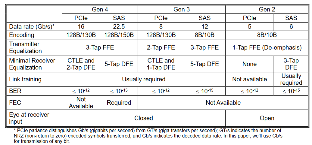
Many standards, including Ethernet, address the problems caused at higher signal frequencies by using complicated coding schemes like PAM4 (4-level pulse amplitude modulation) that combine more than one bit into each transmitted symbol. The latency-sensitive standards discussed in this paper all use the baseband, logic-like NRZ (non-return to zero) scheme.
This paper provides insight into the design and test challenges of Gen4 I/O standards. We begin with a quick review of high speed serial technology that traces signal integrity challenges back to their root causes. We turn to adaptive equalization and link training, and the analysis of closed-eye signals. We show how sophisticated BERTs (bit error rate testers) can virtually probe the performance of integrated receiver components to provide actionable, root cause, debugging information. All of which brings us to FEC, which we describe in conceptual terms sufficient for you to grasp how it works and the challenges it presents. Finally, we conclude with a discussion of the tools necessary to meet the challenges of both compliance and diagnostic testing of Gen4 serial I/O technology.
1. The Challenges of Increasing Data Rates
Figure 1(a) shows a multi-lane enterprise link and Figure 1(b) shows a single lane with the key components. Each lane consists of a low rate, low noise reference clock (typically 100 MHz), a transmitter, a differential channel, and a receiver. In some PCIe designs, the low rate reference clock is distributed from the transmitter to the receiver, called a CC (common clock) configuration. A data-rate clock is recovered from data transitions by a CR (clock recovery) circuit that is integrated within the receiver. The data rate clock sets the sampling time at which the logic decoding circuit/bit slicer identifies bits.

Figure 2 maps the causes of signal integrity problems to their effects and then to the technologies used to address them. Higher data rates mean that signals have higher frequency components and wider bandwidth, faster rise and fall times, and a narrower UI.

The data rate is doubled in the advance from Gen 3 to Gen4 which cuts the UI in half. Measured in UI, the jitter requirements are the same for all generations of PCIe and vary little across SAS generations— which means that jitter margins measured in picoseconds are reduced by factors of two. The tighter UI requires faster rise/fall times which radiates more energy and causes crosstalk.
Reducing the UI by a factor of two also reduces the design margin for differential skew. Differential skew generates common mode noise. To account for skew, the emerging specs introduce a common mode interference term to the stressed receiver tolerance tests. Stressed receiver tolerance tests measure the ability of a receiver to operate at the specified BER with a worst-case but compliant signal.
The response of the channel to signals with high frequency harmonics and a wide bandwidth of subharmonics presents the greatest challenge: frequency and phase dependent signal attenuation due to exponentially increasing PCB (printed circuit board) loss (a.k.a., insertion loss). Since total loss is proportional to channel length, the distance or reach of Gen4 signals on PCB is limited to about 12 inches. The attenuation of the voltage swing and drop in SNR (signal to noise ratio), even after both transmitter and receiver equalization, requires a high sensitivity bit slicer. The Gen4 I/O specs are likely to accommodate post-equalization eye heights of just 15 mV.
2. Channel Response and ISI
Channel response is given by the insertion loss and return loss of the differential channel as a function of frequency. Typical channel responses have two major features: a low pass characteristic that drops exponentially with frequency and nonuniform structure that includes absorption and resonant peaks. The low pass nature is caused by the frequency dependence of dielectric loss and effective resistance due to the skin effect. The resonant/absorption structure is caused by impedance matching difficulties at high frequencies.
The frequency components of NRZ waveforms have tightly knit phase and amplitude relationships. The channel response disrupts these phase-amplitude relationships and causes eye-closing ISI (inter-symbol interference).
3. Equalization
The extreme ISI at Gen4 data rates requires equally extreme equalization technologies. The signal at the receiver input of Gen4 technologies is a closed eye that is qualitatively indistinguishable from noise. Equalization attempts to remove ISI at both the transmitter and receiver. Transmitter equalization distorts the signal in a way that partially counters the channel response. Receiver equalization consists of a combination of linear and nonlinear schemes that attempt to invert the channel response so as to present an open eye to the bit slicer.
Gen4 specs require dynamically adaptive equalization: coordination between the transmitter and receiver called link training that adapts the equalization scheme to operating conditions. Link training presents a huge challenge to test equipment.
BERTs have always been composed of precision clocks driving instrument-quality pulse pattern generators that provide signals to test devices with sensitive error detectors that identify signals, match them to the transmitted patterns and count errors. To test Gen4 I/O technology, BERTs must also be protocol-aware: signals must follow protocol formats and pattern generators and error detectors must be able to submit commands to test devices and respond to commands from test devices.
The BSX-series of BERTScopes were designed to accommodate Gen4 testing.
3.1 Transmitter de-emphasis is generalized to FFE
Early generation serial I/O standards used a simple form of transmitter equalization called de-emphasis. The idea is to counter the low pass nature of the channel response by increasing the relative amplitude of bits prior to logic transitions while holding the overall power constant. At higher data rates, de-emphasis is insufficient and must be generalized to FFE (feed-forward equalization), Figure 3. FFE distorts the transmitted signal in such a way that the channel response yields a cleaner signal at the receiver.
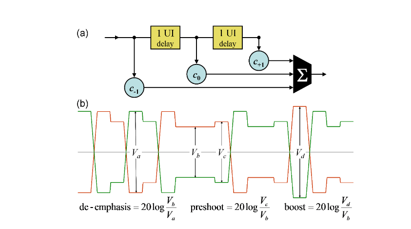
Figure 3 shows “three tap” transmitter FFE; the amplitudes of the three bits surrounding and including transition bits are modified by factors called taps. In PCIe terms, the relative amplitude of bits prior to transitions are increased by a preshoot tap, transition bits are increased by a boost tap, and bits separated by one UI from transitions are de-emphasized.
Transmitter emphasis can be applied in varying amounts to any number of symbols prior to or following a transition. Gen4 technology usually requires 2 to 4 tap transmitter FFE.
3.2 Receiver CTLE and DFE
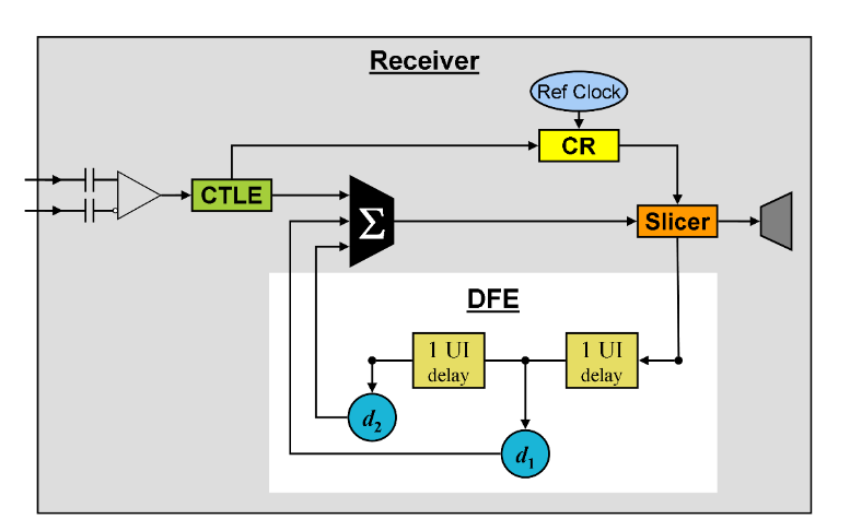
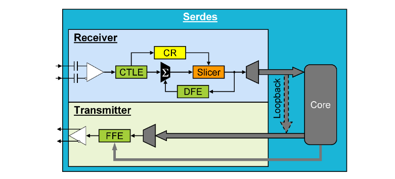
The receiver, Figure 4, has essentially become a black box containing a CR (clock recovery) circuit, two types of equalizers, and the bit slicer none of which are accessible to engineers.

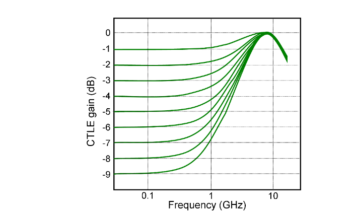
Receiver equalization usually includes both CTLE (continuous time linear equalization) and DFE (decision feedback equalization). CTLE is a linear filter applied to the AC coupled receiver input prior to clock recovery with response controlled by a single gain parameter. As shown in Figure 5, CTLE suppresses the relative contributions of low frequency signal components and amplifies high frequency signal harmonics. The post-CTLE waveform must have sufficiently resolved edges for the CR to recover the data-rate clock.
The recovered clock sets the sampling point of the bit slicer. The identified bits are fed back to the DFE, Figure 6. A DFE is a nonlinear filter that feeds decoded bit values through a shift register. The logic values are delayed, multiplied by taps, and fed back to the slicer to further reduce ISI. Since DFE performance assumes the accuracy of the bit slicer, bit errors can corrupt the DFE output. The corrupt DFE output becomes an additional source of ISI when it is fed back and combined with the next bit presented to the slicer. This next bit is then more likely to be misidentified which further corrupts the DFE output, and so on, often causing error bursts.
The Gen4 standards specify BER performance but do not impose conditions on receiver equalization design.
3.3 Adaptive Equalization and Link Training
Every time the data rate is increased, choices have to be made to maintain performance while optimizing cost. The standards demand greater serdes performance while continuing to use standard circuit board media without introduction of new, higher performance connectors. For example, PCIe Gen4 doubled its data rate without changing the minimum performance requirements of the transmission path.
To accommodate Gen4 data rates on legacy infrastructure in situations where the transmitter, channel, and receiver each come from different manufacturers, the equalization schemes at the transmitter and receiver must be coordinated and must adapt to operating conditions.
To coordinate the collective link equalization scheme, the receiver must be capable of (1) gauging the quality of the connection and (2) modifying the transmitter FFE and receiver equalization parameters.
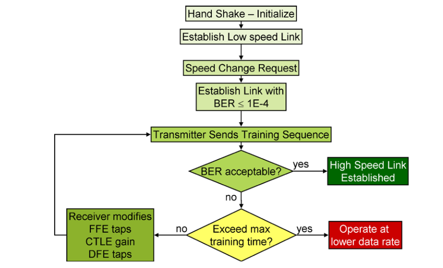
Here’s how it works, Figure 7:
On power up, or whenever the link exceeds the maximum allowed BER, the two serdes exercise a protocol handshake and establish communication at a low data rate, say Gen 2. The receiver of one serdes then submits a speed change request to the other.
The transmitter starts with a preset FFE configuration. For example, PCIe Gen4 transmitters have presets called P0, P1, …, P10 that each consist of pre-determined pre-shoot, boost, and de-emphasis taps. The data rate is advanced to the next generation rate, say Gen 3, and the link is established at BER ≤ 1E-4.
Once the transmitter and receiver complete the initialization, the transmitter sends a known training sequence. The receiver gauges its own performance in some way: through CRC (cyclic redundancy checksums), through FEC, or through built-in system test. The receiver applies an equalization optimization algorithm that tunes both transmitter and receiver equalization parameters. The process continues until the link BER either meets the requirement or fails in the allowed maximum time. If the BER satisfactory, then the system advances to the next higher data rate, say, Gen 3 to Gen4, and repeats the process.
The link will operate at the highest rate for which it can achieve the specified BER.
Even with dynamic adaptive equalization, data transmission across long distances usually requires retiming. Retimers are extension devices that consist of simplified receiver-transmitter pairs with fixed transmitter de-emphasis and receiver CTLE that must accommodate the link training protocol in a limited but transparent way and pass the same tests as any other serdes.
3.4 Link Training Challenges Test Equipment
To test link training, whether for debugging or for compliance, test equipment must be protocol aware: It must blur the line between a BERT and a protocol analyzer. For transmitter tests, the reference receiver must be able to communicate with the test transmitter. For receiver tests, the reference transmitter must be able to communicate with the test receiver.
Due to their complexity, receiver testing is more demanding than transmitter testing. To test link training, the reference transmitter must be able to assemble test patterns into protocol blocks, apply the data encoding scheme, like 128B/130B, scramble the data, execute the communication initialization handshake, respond to the test receiver’s requests for different FFE taps, and meet response time requirements.
Testing and debugging the reference transmitter-test receiver handshake can be difficult. The ability to create stimulus/response scenarios and monitor how the test receiver responds to pattern sequences provides a key window to receiver performance during the handshake.
For transmitter test, the reference receiver must request different sets of taps as specified in the standard. At a bare minimum, the reference receiver must be able to convey to the test transmitter whether or not the equalization negotiation process yielded a successful link.
4. Trends in Channel Performance Evaluation
In addition to equalization, S-parameter restrictions are imposed to limit problems caused by the channel response. S-parameters describe the frequency and phase response of passive devices like traces, cables, and connectors as well as the input and output responses of transmitters and receivers.
Gen4 standards use S-parameter masks to limit the insertion loss (Sdd21), return loss (Sdd11 and Sdd22), ILD (insertion loss deviation), differential-to-common mode conversion in both transmission and reflection (Scd21, Scd11, and Scd22), and crosstalk.
4.1 Crosstalk
At lower data rates, differential signaling was sufficient to mitigate crosstalk concerns. At Gen4 data rates, crosstalk can not be neglected.
Crosstalk comes from electromagnetic radiation during the logic transitions of an aggressor. It appears on a victim channel as jolts of high frequency noise. In systems where lanes are synchronized, crosstalk appears at a fixed time-delay region of the eye diagram with a duration that’s about the same as the aggressor rise/fall times. In systems that are not synchronized, the timing of crosstalk varies across the eye.
Since transmitter FFE and receiver CTLE amplify the relative contribution of high frequency signal content, they also aggravate crosstalk. DFE, on the other hand, doesn’t affect crosstalk either way. Link training provides a dynamic way for systems to optimize the FFE-CTLE-DFE-crosstalk balance Since crosstalk is worse in systems with high insertion loss, standards allow designers to balance crosstalk and loss impairments through insertion loss to crosstalk ratio vs frequency, ICR(f) or with a compliance template for ICN (integrated crosstalk noise) vs IL (insertion loss) at the Nyquist frequency.
4.2 The Trend Toward Channel Performance Modeling
Another important trend in the advance beyond 15 Gb/s is the use of complicated algorithms that combine the effects of channel response, crosstalk, and equalization on BER performance. At lower rates, requirements on the maximum allowed insertion loss and crosstalk were sufficient to assure interoperability of channels with compliant serdes. At Gen4 rates, the effect of equalization must be included because of the complicated way it can affect crosstalk.
The trend toward combining many design parameters into a single figure of merit is meant to expand design choices and allow engineers greater scope in cost-performance optimization.
The idea is to construct a model of channel performance that combines crosstalk with transmitter noise and jitter. A fast iterative procedure determines an optimal equalization scheme for a compliant transmitter. The model uses a minimal reference equalization scheme and a worst-case but compliant transmitter model to estimate the eye height and eye width at the input to the bit slicer.The modeled channel BER performance must be better than a specified minimum. Typically, systems that don’t use FEC require BER < 1E-15 if transmitter noise is not included in the model or BER < 1E-12 if transmitter noise is included in the model.
Another Gen4 approach is called “channel tolerancing.” Channel tolerancing is a procedure built into serdes that performs dynamic eye height and eye width measurements for a given channel-equalization combination.
5. Debugging Receivers of Closed Eyes
The signal at the receiver pins is a closed eye. We can model the performance of the receiver’s internal components its AC coupled input, CR, CTLE, DFE, and slicer, shown in Figure 4 but we can’t probe them because the reference points are inside the chipset. The only signal we can access is the retimed signal from the receiver operating in loopback mode, Figure 8.
When debugging, the situation can seem hopeless, but BERTs have a unique and often misunderstood ability to virtually probe every component within the receiver.
A well-equipped BERT like one of Tektronix’s BSX-series BERTScopes has three key features necessary for debugging Gen4 receivers: First, the BERTScope pattern generators can transmit any user-defined test pattern up to 528 Mb long or a variety of PRBSn (pseudo-random binary sequence) test patterns. Second, BERTScope pattern generators can transmit signals impaired by precise levels of several different signal stresses. And, third, the BERTScope’s Error Location Analysis tool determines the exact locations of bit errors and assembles them into myriad distributions that indicate different types of correlations with block lengths, time scales, the transmitted pattern, lengths of burst errors, error free intervals, and configurable error maps.
Combinations of test patterns and signal stresses can be configured that target each component within the receiver black-box to virtually probe AC-coupling, CR, CTLE, DFE performance, and slicer sensitivity. When we know that a signal stresses one component more than the others we can use Error Location Analysis to identify the faulty component and its operating margin.
6. Gen4 Stressed Receiver Tolerance Testing
Stressed receiver tolerance tests are designed to assure that every compliant receiver can operate at the specified BER with the worst-case but compliant input signal.
Gen4 standards consolidate separate jitter and voltage tolerance tests into a single stressed jitter tolerance test. The test is performed with the reference transmitter FFE settings set by the link training negotiation described in Section 3.3. The applied stresses include ISI-causing channel response from compliance test boards, RJ (random jitter), both common and differential sinusoidal interference, all sources of asynchronous crosstalk, and swept SJ (sinusoidal jitter). Since the test fixture—cables, connectors, splitters, etc—causes DDJ (data-dependent jitter) that is very difficult to accurately de-embed, Gen4 standards include the test fixture among the applied stresses.
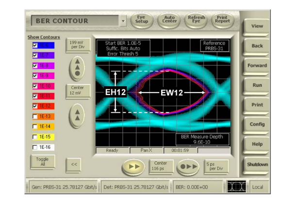
Rather than specify a tolerance test signal at the receiver pins, Gen4 standards specify the total applied stress in terms of the post-equalization EH (eye height) and EW (eye width) at the bit slicer.
EH and EW are each measured with respect to BER. EH12 is the vertical opening in mV and EW12 is the horizontal eye opening in UI or ps of the BER=1E-12 contour, Figure 9.
The stressed receiver tolerance tests are applied across an SJ template like those shown in Figure 10. A compliant receiver should operate at or better than the required BER for every frequency across the SJ template.

6.1 Calibrating the Stressed Eye – Trend Toward Modeling
Since measuring EH and EW within the receiver chipset is impossible, fast, statistical simulation models are used to calibrate the stressed eye.
The model uses specified transmitter voltage swing and rise/fall times plus the applied stresses along with measurements of the channel S-parameters, including the test fixture. The model finds the optimal equalization parameters assuming the minimal reference receiver equalization scheme and then estimates EH and EW at the slicer. If EH and/or EW are too large, then additional stresses can be applied, like RJ, increased voltage noise, and/or the transmitted voltage swing can be reduced. Similarly, if EH is too small, then the voltage swing can be increased.
7. BER and FEC Forward Error Correction
FEC is required to meet the SAS Gen4 BER requirement. When conditions are so severe that a Gen4 receiver cannot operate at the specified BER, then FEC can be employed. FEC can relax the raw BER requirement by a factor of a million or more but at the cost of 2-15% additional bandwidth overhead, depending on the specific FEC implementation. FEC also increases latency, requires extra power, and can complicate BER analysis.
FEC encodes blocks of the signal with extra parity-like bits. The number of errors that an FEC scheme can correct depends on the order of the errors within each block. The maximum and minimum number of correctable errors can vary by a factor of ten or more.
The Reed-Solomon FEC scheme used in SAS Gen4, called RS-FEC(30, 26), can correct at most 10 bits out of 130 but, depending on their order, as few as 2, at a bandwidth overhead of about 13%.
Since systems with DFE tend to suffer burst errors that can overwhelm FEC, some standards use datainterleaving or data striping to redistribute burst errors across blocks. With fewer errors in each block, FEC can be more efficient.
7.1 Converting Raw BER to FEC BER
Since the order of the errors within each block severely affects FEC performance, it can be very difficult to estimate the post-FEC BER from the raw pre-FEC BER. BSX-series BERTScopes use Error Location Analysis tools to measure both.
By identifying the locations of every error the BERTScope seamlessly translates the raw pre-FEC BER to the corrected post-FEC BER even when the data is interleaved.
8. Conclusion
The proliferation of high speed serial I/O technology like PCIe and SAS and its advance to Gen4 data rates makes it a cost-performance optimized data center connectivity solution. The introduction of link training is the most disruptive trend in the emerging Gen4 standards and not just for the engineers who design, test, and implement the technology, but for the companies that develop test equipment for those engineers.
Since BER is the single most important performance criterion of a digital system, BERTs have always played a crucial test role. In the past, BERTs provided instrument quality pattern pulse generators with pristine clocks and error detectors with state of the art sensitivity. The need to test and debug the link training process demands that BERTs also be protocol aware.
The BERT pattern generator and error detector must be capable of communicating as defined by each standard’s protocol. The pattern generator must be able to initiate loopback mode in a test receiver. The error detector must be able to communicate the quality of reception back to the pattern generator. The pattern generator must be able to respond by adjusting the transmitter equalization scheme within the constraints of the standard. Rather than transmitting simple test patterns, the pattern generator must be able to assemble data into blocks consistent with the standard’s protocol and the error detector must be capable of decoding them.
BER is the unquestioned judge of both component and system performance and is the ultimate compliance requirement, but BERTs are often ignored as debug tools. Since BER is a single number, many engineers don’t realize that BERTs can provide actionable, diagnostic, root cause information. We’ve seen that, at least for a well outfitted BERT like a BSX-series BERTScope, BERTs can be formidable Gen4 diagnostic tools, as long as they include these key features:
- Data rates up to 32 Gb/s with instrument-quality pattern generators capable of at least 3 taps of FFE and fine error detector sensitivity, at least 15 mV.
- Protocol-aware pattern sequencing, scrambling, encoding, etc.
- The ability to program stimulus/response scenarios and generate external triggers for oscilloscopes or logic analyzers.
- The capacity to transmit a wide variety of programmable test patterns tailored to target the performance of specific components within the black-box of complex Gen4 receivers.
- The ability to apply a wide variety of precise levels of signal stress including RJ, SJ, DM-SI, CMSI, F/2, and ISI.
- Error Location Analysis that measures both raw pre-FEC and post-FEC BER.
- The ability to virtually probe the margins of components within the serdes chip by combining carefully chosen pattern-stress combinations with analysis of Error Location Analysis distributions and correlations.

BSX-series BERTScopes have all of the features necessary for both compliance testing and debugging Gen4 serdes plus the BERTScope signal analysis tools that you’re accustomed to like eye diagrams, BER-contours, and bathtub plots.

