1. Introduction
High speed, scalable connectivity solutions like PCIe (Peripheral Component Interconnect Express) and SAS (Serially Attached SCSI) are rapidly becoming the preferred choice for local storage and I/O in data center as well as enterprise computing applications. The bandwidth provided by Infiniband and Ethernet no longer compensate for their latency, power, and cost demands in the face of scalable 15+ Gb/s per lane commodity high speed serial Gen4 PCIe and SAS I/O solutions.
The receivers used in Gen4 serial I/O technology include complex integrated components that are not directly accessible for testing: the clock recovery circuit cannot be probed, the performance of the equalization schemes cannot be observed directly, and the sensitivity of the logic decoder cannot be measured. We're left with a black box that, more than any other part of a serial link, determines system performance.
In this paper, we show how to perform compliance and diagnostic tests for the Gen4 receivers. BERTs (bit error ratio testers) have a reputation for judging standards compliance without providing actionable debug information. By measuring BER, they do indeed provide the conclusive measure of performance but, as we'll see, Tektronix's BSXseries BERTScopes are sophisticated tools that can scramble and encode transmitted signals, exercise protocol-driven processes, and isolate the performance of each receiver component.
The new and emerging Gen4 I/O standards bring new receiver test challenges:
- Link Training: Adaptive equalization that requires coordination of the receiver and transmitter to optimize the equalization scheme for each link at power up and in recovery.
- The ability to tolerate common mode as well as differential mode noise.
- NRZ (non-return to zero) symbol decoders/bit slicers with 15 mV sensitivity.
- FEC (forward error correction) that can relax BER requirements but make interpreting BER measurements tricky.
- Use of complicated reference receiver models for calibrating compliance test conditions.
Some standards address the problems caused by high signal frequencies with coding schemes like PAM4 (4-level pulse amplitude modulation) that combine more than one bit in each transmitted symbol. The standards discussed in this paper all use the baseband, logic-like NRZ signaling scheme.
We begin by looking at the roles of each internal component of high speed serial receivers and then turn to the new concept of adaptive equalization and protocol-aware link training. With the technology in hand, we continue to receiver debug techniques and the stressed eye tolerance tests required by Gen4 standards.

2. Elements of Gen4 High Speed Serial Receivers
High speed serial links consist of four essential components: a reference clock, a transmitter, a channel, and a receiver in a multi-lane architecture like that shown in Figure 1.
The reference clock serves as the time base for the serializer and transmitter. The transmitter applies FFE (feed-forward equalization) to differential signals. The channel consists of everything between the transmitter and the receiver including pins, connectors, traces on PCB (printed circuit board), vias, cables, etc. The task of the receiver is to identify bits at or better than the specified BER after the transmitted waveform has suffered frequency-dependent loss, crosstalk, random jitter and noise, and any EMI (electromagnetic interference) in the system. At the receiver input, eye diagrams are closed.
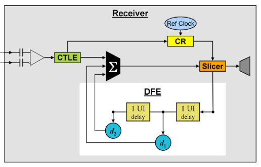
To accomplish their formidable task, Gen4 high speed serial receivers include several complex, interrelated components, Figure 2: An AC coupled differential input to a comparator. The CTLE (continuous time linear equalizer) accepts the comparator input and removes some of the ISI (inter-symbol interference). The CR (clock recovery) circuit recovers a data rate clock from the waveform and sets the time-delay position for the bit slicer. The slicer identifies 1s and 0s. The decoded signal is split; one output is directed to the serdes core and the other output loops back to the DFE (decision feedback equalizer). The DFE feeds decisions back to the slicer input in a way that removes more ISI.

Since the components are integrated in the serdes chip, receivers are essentially black boxes. The inability to directly probe each component makes them notoriously difficult to troubleshoot.
The specified maximum BER allowed performance is typically 1E-12 or 1E-15. FEC can provide relief from the difficulty of decoding closed eye signals by reducing the raw BER requirement by a factor of a million, but FEC requires more bandwidth, power, and latency.
3. Adaptive Equalization and Link Training
The biggest problem at high data rates is caused by the channel response; that is, the frequency and phase dependence of signal loss. The loss at the Nyquist rates for either PCIe Gen4 or 22.5 Gb/s SAS exceeds 24 dB, but the gross loss is just part of the problem.
A digital waveform is defined by the relationships between the amplitudes and phases of each signal component. An ideal NRZ signal would consist of a digital-looking square wave with at most three harmonics and as many subharmonics as are permitted by the data scrambling and encoding schemes, but the frequency dependence of the insertion loss decouples the Fourier components of the signal and causes eye-closing ISI. Add frequency-dependent reflections and you can see why Gen4 data rates demand highly optimized equalization schemes.
Multi-tap FFE is required at the transmitter and the receiver performance must perform at least as well as a behavioral reference receiver defined by the standard; a combination of CTLE with adjustable gain and/or 2 to 5 tap DFE. Gen4 performance criteria require coordination between signal conditioning at the transmitter and the receiver to optimize each link's equalization scheme. This type of adaptive equalization is called "link training" or "speed negotiation" and must accommodate the ability to recover should the link BER exceed the maximum allowed during operation.
Since FFE and CTLE can increase crosstalk, link training must maximize the improvement of ISI while minimizing the impact of crosstalk. With FFE taps, CTLE gain, and DFE taps, link training is a multi-dimensional optimization process that requires communication between the transmitter and receiver.
3.1 EQUALIZATION—FFE, CTLE, DFE
Equalization is a scheme for correcting the ISI caused by the channel response. Since the glaring feature of the channel response is its low pass filter quality, the simplest equalization schemes de-emphasize low frequency signal components, emphasize high frequency components, or both.
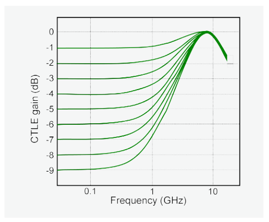
Receiver CTLE is a filter that attenuates low frequencies, passes high frequency signal harmonics, and attenuates high frequency noise. CTLE filters have a fixed low frequency pole, a fixed high frequency pole, and adjustable DC gain, gCTLE, as shown in Figure 3. The poles are typically and , where fd is the data rate and gCTLE is a single parameter that is adjustable in 1 dB steps.
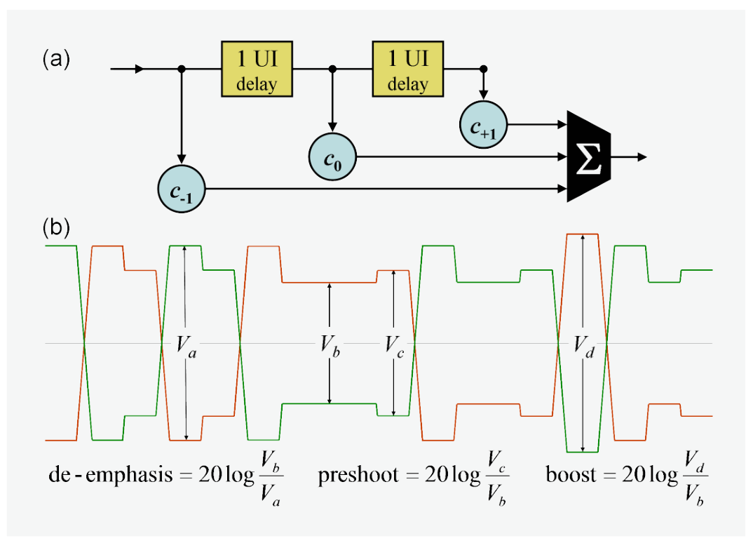
The simple transmitter de-emphasis that was sufficient at lower data rates used a single tap of equalization; that is, bits that underwent logic transitions were transmitted at greater relative amplitudes than others. At Gen4 data rates, transmitter equalization has been expanded from that single tap of deemphasis to multi-tap FFE. Multi-tap FFE, Figure 4, applies taps in a way that distorts the transmitted signal so that the channel response serves to equalize it.
DFEs are shift registers, Figure 5, that multiply delayed logic decisions with taps, combine them, and feed the results back to the incoming post-CTLE waveform as in Figure 2. Since DFEs operate on logic values rather than voltages, they are nonlinear filters.
While DFEs are remarkably effective at reducing ISI and opening eye diagrams, they are also susceptible to burst errors. When a bit is misidentified, the output of the DFE is corrupted which may cause another error. That second error is likely to cause a third, and, so on. FEC schemes are chosen that can accommodate burst errors, but as we'll see in Section 4, it's tricky
3.2 PROTOCOL-AWARE LINK TRAINING
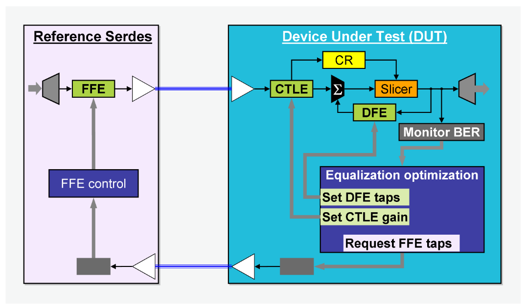
Adaptive equalization requires feedback between two serdes: the downstream port whose transmitter FFE coefficients are being trained and the upstream port whose receiver equalization parameters—CTLE gain and/or DFE taps—are being trained. In the context of receiver testing, the DUT (device under test) is identified as the upstream port and the BSX-series BERTScope plays the role of the downstream port or reference serdes.
The BSX-series BERTScopes have the protocol-aware abilities necessary for testing and analyzing the link training process at both the DLL (data link layer) and PHY (physical media) layers: They can sequence, scramble, and encode test patterns according to the protocol; they have pattern generators with multi-tap FFE that can be adjusted by the DUT; and they recognize commands from and can submit commands to the DUT.
Link training protocol is governed by state machines that differ for each standard but follow this general description:
Phase 0:
- The DUT and the reference serdes enter the recovery or speed negotiation state due to powering on, a hard reset, loss of synchronization, a hot plug timeout, etc.
- The DUT and reference serdes execute a handshake to synchronize and align with each other. They then exchange timing and setup parameters like maximum allowed speed negotiation and training times, lane polarity, link numbers and so forth. They also exchange PHY capabilities that include their abilities to modify either or both of their receiver and transmitter equalization schemes.
- With the handshake complete, the DUT submits a speed change/link equalization request.
Phase 1:
- Transmitters are pre-loaded with several sets of transmitter FFE taps called presets, PCIe has 11 such presets. The reference transmitter starts with either default values, a preset, or the most recently trained FFE taps.
- The data rate is advanced and the link is established at BER ≤ 1E-4.
Phase 2:
- The reference serdes transmits protocol-based training sequences.
- The DUT receives the known training sequences and measures its BER. There are several ways that a serdes might measure its BER performance: CRC (cyclic redundancy check) values, the CRC is typically 32 bits long; FEC-based error counting; or through its own internal error detector.
- If the BER is acceptable then the state machine proceeds to Phase 3. Acceptable BER depends on the standard, either less than or equal to 1E-12 or 1E-15; if FEC is implemented then that maximum can be the post-FEC BER.
- If the BER is not acceptable but the maximum link training time has not been exceeded, then the DUT makes specific requests to alter the test transmitter FFE taps: increment, decrement, leave unchanged, or install another preset. The reference transmitter adjusts its FFE taps and resumes transmitting training sequences.
- After each modification of the reference transmitter scheme, the DUT applies an algorithm to optimize its own receiver equalization parameters, e.g., CTLE gain and/or DFE taps.
- If the system can't find an equalization scheme that delivers acceptable BER performance in the allowed training time, or if it loses synchronization for any reason, then the training is marked invalid and the system reverts to a lower data rate and may or may not attempt another recovery
Phase 3:
- The roles of the upstream and downstream ports are reversed and the downstream (DUT) transmitter FFE taps are trained by the upstream (reference serdes) transmitter.

3.3 RECEIVER LINK TRAINING TEST
The receiver link training test determines whether or not the DUT is capable of negotiating a successful link.
The link training test is initialized with a handshake that puts the DUT receiver in the L0 or recovery state. The protocolaware pattern generator must put the receiver in loopback mode. Loopback mode directs the receiver output signal to the serdes' transmitter without modification, as shown in Figure 7.
Problems associated with the handshake between the receiver and transmitter that initializes link training in Phase 0 can be difficult to diagnose. The BSX-series BERTScopes allow you to create stimulus-response test conditions. For example, the BERTScope transmitter can increment the sequencer to send a sequence of commands that ought to generate specific responses from the DUT; you can configure the BERTScope error detector to recognize patterns from the DUT and generate an external trigger for an oscilloscope or logic analyzer.
Phase 1 and Phase 2 proceed with the DUT commanding the BERTScope to alter its transmitter FFE taps according to the protocol until the DUT receiver verifies that its operating BER is no larger than that required. The BERT error detector then confirms the BER performance by analyzing the retimed loopback signal.
The test should be repeated for different initial transmitter FFE presets to confirm that the receiver equalization training algorithm is robust to different initial conditions.
4. FEC—Forward Error Correction
FEC is not required in most I/O standards but is usually an option in Gen4 when the required BER can't be met without it. FEC adds several parity-like bits to fixed-length sets of signal bits. The combinations of data and parity bits form codewords. Codewords are encoded by a shift register in such a way that, at the receiver, a complementary shift register can decode the word and correct some errored bits. The number of bits that an FEC scheme can correct depends on the order of the errors within each codeword.
Reed-Solomon FEC is a common scheme in high speed serial applications. RS-FEC(n, k) is a block coding scheme that appends 2t parity-like symbols to k data symbols to make a total codeword of k+2t=n symbols, Figure 8. In this context, symbols are composed of m contiguous bits where m is usually chosen in a way that is consistent with the protocol packet or word definition.
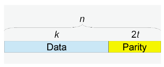
RS-FEC can correct up to t symbol errors in each codeword. It's important to note that all of the bits in each of the t symbols can be corrected, but if single errors occur in more than t symbols, RS-FEC cannot correct any of them. The maximum number of correctible errors is therefore mt and the minimum is t. A specific example should help clarify:
SAS Gen4 uses five bit symbols in an optional RS-FEC(30, 26) scheme; 30 symbols are composed of a total of 30•5=150 bits that encode 26•5=130 bits of data. RS-FEC(30, 26) can correct at most t=2 symbols which corresponds to a maximum of 10 and a minimum of 2 bit errors out of each 130 data bits. But that maximum can only occur when all 10 errors align perfectly in two separate symbols.
With 2t = 4 parity symbols, we have 20 bits of FEC overhead, giving RS-FEC(30, 26) a bandwidth overhead of 2t/n = 4/30 which is about 13%.
Another common FEC choice is RS-FEC(528, 514) which encodes 5140 data bits in 528 ten bit symbols and can correct a minimum of 7 errors and a maximum of 70 at a cost of just under 3% overhead.
In Section 3.1 we saw that the downside of DFE is its tendency to generate burst errors. The ability of RS-FEC to accommodate error bursts makes it a good choice. Still, if the bursts are too long, then RS-FEC won't help. Interleaving data from separate lanes, or data striping, prior to FEC processing splits up strings of burst errors into separate codewords. If the raw BER is low enough, say 1E-6, then distributing burst errors into separate codewords can all but guarantee post-FEC performance of 1E-15.
In any case, engineers who try to estimate the post-FEC BER from a measured raw, pre-FEC BER face a formidable challenge due to the order-dependence of the number of correctible errors. Interleaving can further aggravate the conversion from pre-FEC to post-FEC BER. Fortunately, Tektronix BSX-series BERTScopes equipped with the FEC Emulation feature measure both pre and post FEC BER.
4.1 ERROR LOCATION ANALYSIS CONVERTS RAW BER TO FEC BER
FEC emulation is a BERTScope feature built on Error Location Analysis that monitors the exact locations of detected errors according to user-defined FEC parameters. When errors occur within correctable symbols, they're treated as though they have been corrected; in other words, the post-FEC BER is calculated only from errors that the FEC scheme can't correct.
To set up an RS-FEC(30, 26) scheme, just define the parameters:
Architecture: one-dimensional
symbol size = 5-bits
n = 30
k = 26
t = 2
The architecture parameter is "one-dimensional" in the sense that a single stream of codewords is processed by the RSFEC(30, 26) scheme. To emulate a simple interleaved system, the architecture should be set to "two-dimensional." For example, to emulate RS-FEC(30, 26) encoded data interleaved across four lanes:

The t = 0 setting in the outer code indicates that the act of 4-way interleaving does not contribute additional FEC.
With the knowledge of error locations and FEC codeword structure, the BERTScope reliably measures the post-FEC system performance. You can also experiment with different FEC schemes to find one that optimizes the BER performance, overhead, power, and latency for a specific application.
Error Location Analysis also provides key diagnostic information in receiver test, especially when coordinated with the application of specific signal impairments.
5. Gen4 Receiver Debug and Diagnostic Testing
In this section, we focus on test techniques that reveal the performance of individual components within the receiver.
The BERTScope can transmit any test pattern up to 528 Mb in length, with or without protocol-specific coding and packet and block structure, as well as all of the standard PRBSn (pseudo-random binary sequences of length n) patterns. The BERTScope can also apply precise levels of several signal impairments, Figure 9.
We can probe specific internal components by submitting the receiver to combinations of test patterns and stresses carefully chosen to target the performance of those components. If we start to see bit errors, then we've found that component's performance margin. By using Error Location Analysis we can usually a problem's root cause.
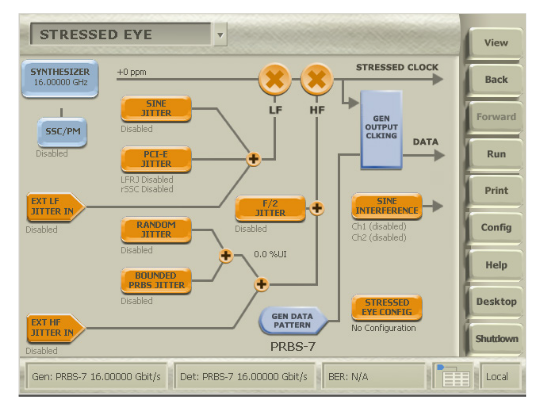
In the following sub-sections, we'll give examples of how to probe the performance of specific receiver components. An exhaustive debug strategy is beyond our scope, but these examples will give you concepts that can expand your debug strategies.
5.1 AC COUPLED DIFFERENTIAL INPUT
The differential input to the receiver is AC coupled to a comparator. AC coupling sets the baseline voltage for the bit slicer. High speed serial I/O standards use data scrambling and encoding to assure 50% mark density over data sequences on the scale of the AC-coupling time constant.
To probe the AC coupled input, use a clean signal with no applied stress and a test pattern with, first, very low mark density, something like 0010 repeated many times and followed by an easy pattern, say PRBS5. The idea is to encourage drift with a test pattern that has low mark density but high enough transition density that the CR is not challenged. You shouldn't see errors until the time duration of the low mark density sequence exceeds the time constant of the input coupling.
Repeat the test with a very high mark density test pattern like repeating 1101 sequences. The onset of burst errors should occur at roughly the same point in the pattern for both the high and low mark density patterns. If it doesn't, there's an input asymmetry
5.2 CR—CLOCK RECOVERY
The CR circuit recovers a data-rate clock from the waveform after it has been conditioned by the CTLE. CRs are typically based on DLL (data-locked loop) or PI (phase interpolator) designs that have well defined bandwidths. The CR sets the time-delay position of the bit slicer sampling point. Systems that recover clocks from the data are also called embedded or forward clocking.
To recover a clock, the CR needs a signal with plenty of logic transitions. Standards require 50% transition density, scrambling, and data encoding; PCIe Gen4 uses 128B/130B and SAS 22.5G uses 128B/150B encoding.
To test the ability of a CR to recover and lock a clock signal, isolate it from equalization problems by testing without extra ISI and with the CTLE gain set to zero. When the CR loses its clock, the bit slicer is mistimed and generates burst errors.
To probe basic CR performance, submit it to signals with long strings of CIDs (consecutive identical bits). The CR should be able to recover and lock a clock on any signal that has both 50% transition density and the maximum string of CIDs permitted by the standard.
To probe a CR's bandwidth and jitter filtering performance, submit the receiver to test patterns with plenty of transitions, like PRBS7, and add high amplitude SJ (sinusoidal jitter).
The data jitter whose frequency is below the CR bandwidth will also be present on the recovered data-rate clock. The jitter that is present on both the signal and the timing of the slicer's sampling point cannot cause errors. The CR should maintain lock until the SJ frequencies pass its bandwidth roll-off at which point BER will increase. By analyzing the error free interval histogram provided by Error Location Analysis you can confirm that the onset of errors coincides with the extreme SJ swings.
One aspect of PCIe that makes it unique among the I/O standards is that it accommodates a distributed reference clock. In the "common clock" architecture, a 100 MHz reference clock is distributed from the transmitter to the receiver of a PCIe lane. At the transmitter, a PLL (phase locked loop) multiplies the reference clock up to the data rate. At the receiver, the reference clock serves as the local oscillator for the CR circuit. The jitter transfer function of these common clock receivers depends on the difference function between the transmitter PLL and receiver CR and the transport delay between the receiver and transmitter.
The CR bandwidth must be higher than the frequency of any applied signal modulation like SSC (spread spectrum clocking). SSC is used to reduce power radiated at a single frequency, usually to help the part meet government communications regulations. The most common SSC is 33 kHz triangle-wave frequency modulation with amplitude of less than or about 0.5%. The CR should easily filter SSC.
To test a CR's resilience to SSC, increase the SSC amplitude. The receiver should not experience errors until the SSC amplitude generously exceeds the maximum permitted for a compliant signal.
5.3 EQUALIZATION—CTLE AND DFE
To probe equalizer performance, apply ISI by transmitting test patterns that have a lot of structure through long traces on test boards. Every permutation of 1s and 0s within the time-duration of the channel's pulse response generates uniquely shaped logic transition waveforms. ISI is the set of logic transition shapes. The more varied the structure of a test pattern, the more ISI the channel response excites.
Some transitions are more aggravating than others. The JTPAT (jitter tolerance pattern) and SSPR (short stress pattern random) patterns consist of a long run of low transition density followed by a long run of high transition density and then another short run of low transition density; they were designed to accommodate the limitations of oscilloscopes by generating the maximum ISI in a comparatively short pattern (2240 bits for JTPAT and 32,762 bits for SSPR). Since BERTs aren't limited by signal length, you can analyze any pattern you can conceive up to 528 Mbits or even PRBS31 which includes every permutation of 31 bits even though it's over 2 billion bits long. In most cases PRBS31 excites all the ISI that a receiver will ever see. Even though PRBS31 is long, it repeats at least seven times a second in Gen4 applications, often enough that, if equalization fails you'll see errors and can assemble error distributions and correlations in about a minute.
Since errors caused by equalization problems either CTLE or DFE tend to occur at the same subsequence of the pattern on each repetition, you can isolate them quickly with the pattern sensitivity histogram Error Location Analysis feature. Look for correlated burst errors from DFE failure or small numbers of errors at the same location from CTLE failures.
5.4 LOGIC DECODER/BIT SLICER
The logic decoder or bit slicer distinguishes 1s and 0s at sampling times determined by the recovered clock, ts : If the signal voltage at the sampling time is above the slice threshold, Vs, the bit is identified as a 1, if it's below the threshold it's identified as a 0. Of course the position of the sampling point,(ts, Vs), is not an ideal point, it's a region determined by setup and hold times and voltage-slice sensitivity that consumes both jitter and noise margin.
The sensitivity of the slicer is the minimum voltage swing with which it can consistently distinguish 1s and 0s. The emerging Gen4 standards specify minimum post-equalization EH12 (eye height defined at BER = 1E-12) as low as 15 mV. EH12 is the vertical separation of BER=1E-12 contours like that shown in Figure 10. Receivers with minimal equalization schemes require bit slicers whose sensitivity is better than 15 mV.

Accurate models of the CTLE-CR-DFE combination should give accurate EH and EW estimates. The effective slicer timing margin and voltage sensitivity can then be estimated from its performance as EH and EW are varied by altering combinations of signal stress.
The slicer timing margin is also affected by differential skew. At Gen4 data rates, a few ps of differential skew can introduce common mode noise and cause bit errors. Probe the slicer's resilience to skew by stressing it with an innocuous pattern, like PRBS7 that doesn't encourage drift or challenge the CR. Then apply increasing levels of CM-SI (common modesinusoidal interference) to the signal. If the slicer is particularly sensitive to skew, the BER will go up quickly.
6. Compliance Testing—Stressed Eye Tolerance Tests
The idea of stressed eye tolerance tests is simple: if a receiver can operate at or better than the prescribed BER with the worst-case but compliant signal, then it should operate with any compliant signal from any combination of compliant channels and transmitters.
The most difficult part of a tolerance test is calibrating the signal. Since the eye is closed at the receiver pins and since it's difficult to specify the structure of a closed eye, the tolerance test signal is calibrated by modeling the receiver response. The eye opening, EH and EW, at the input to the bit slicer is estimated by modeling the CTLE+CR+DFE response of a minimal reference receiver to the stressed signal.
6.1 TYPICAL STRESSED EYE COMPLIANCE REQUIREMENTS
Table 1 lists the typical stresses required in Gen4 receiver tolerance tests. Though the calibrated stressed eye includes the stresses listed, the Gen4 PCIe stressed eye is ultimately specified by the post-equalization EH and EW, not the precise levels of individual signal impairments.
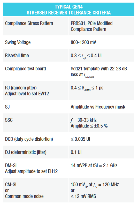

Always check the technology standard for the most accurate, up-to-date requirements. Every standard is unique. Even within PCIe, requirements differ for CEM (card electromechanical) testing and vary depending on whether or not a distributed reference clock is included.
6.2 STRESSORS
The compliance test pattern depends on the standard. PCIe Gen4 uses the PCIe Modified Compliance Pattern which is over 8.5 Mbits. Most other standards use PRBS31. When the test incorporates link training, the link is trained as described in Section 3 and then the trained equalization scheme is used in the tolerance test. Different patterns are used for calibrating the stresses. Repeated clock-like patterns, 0011 0011, are used for calibrating input jitter and JTPAT is sometimes required for calibrating DDJ (data-dependent jitter), the combination of ISI and DCD.
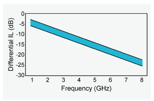
Worst case ISI can be added in any way, provided the differential insertion loss (Sdd21) is bounded by a template like that shown in Figure 11. It's usually generated by compliance test boards, such as CBB (compliance base board) used for PCIe CEM add-in card testing or CLB (compliance load board) for system board testing. The cables, connectors, splitters, etc, that make up the test fixture also contribute ISI. The total nominal loss at the Nyquest frequency, ½ fd, is 28 dB of which about 23 dB comes from the test channel.
Voltage noise is applied through two types of sinusoidal interference, DM-SI and CM-SI. The differential input ought to cancel CM-SI but some differential skew and differential to common mode conversion caused by, for example, multiple reflections can let some in.
6.3 CALIBRATING THE STRESSED EYE
Modeling is necessary to tune the stresses to get the specified EH and EW as it would appear after equalization at the bit slicer of a minimal specified behavioral reference receiver.
It's important to note that the reference receiver clock recovery and equalization schemes are prescribed by the standard. They usually use a single pole PLL (phase-locked loop) CR model and DFE. PCIe Gen4 uses a 1st order CTLE and a 2 tap DFE and SAS 22.5 uses 5 tap DFE, but the actual receiver equalization scheme is the responsibility of the designer.
The eye is modeled by a fast statistical-based simulator, sometimes called waveform post-processing. A Python model called SEASIM is available from the PCI-SIG (Special Interest Group) for BASE testing; SigTest is different tool from PCISIG that's used for both BASE and CEM testing. The models include a transmitted signal, applied stresses, and the channel response right up to the receiver input pins. The SJ frequency is set well above the behavioral CR roll off with amplitude of 0.1 UI.
The simulated transmitter signal can be acquired on an oscilloscope by averaging a few million repetitions of the test pattern or modeled from the voltage-swing and rise/fall times required by the standard's transmitter specification. Signal stresses like those in Table 1 are then added to the waveform.
The channel response is derived from the full differential S-parameter matrix which can be measured or extracted from the pulse response of the channel including everything in the path from the BERTScope pattern generator output to the pins of the receiver being tested.
Crosstalk can be included through multi-channel S-parameters or by the measured peak-to-peak crosstalk voltage. The model optimizes the transmitter FFE taps and the reference receiver CTLE gain and/or DFE taps to get the largest eye opening possible from which values for the EH and EW are produced.
Small adjustments to the transmitted voltage swing and/or applied RMS RJ (random jitter), DM-SI, and/or SJ stresses are usually necessary to tune the EH and EW to the required values—PCIe Gen4 requires EH12 = 15 mV and EH12 = 0.3 UI to within 15%.
6.4 THE STRESSED EYE TOLERANCE TEST
Configure the BERTScope transmitter with the stresses that resulted from the calibration procedure. The receiver can either report BER itself or be configured in loopback mode so that the BERTScope measures BER. The transmitter FFE taps derived during eye calibration can be used for a minimal tolerance test, but including link training in the process is a more complete test.
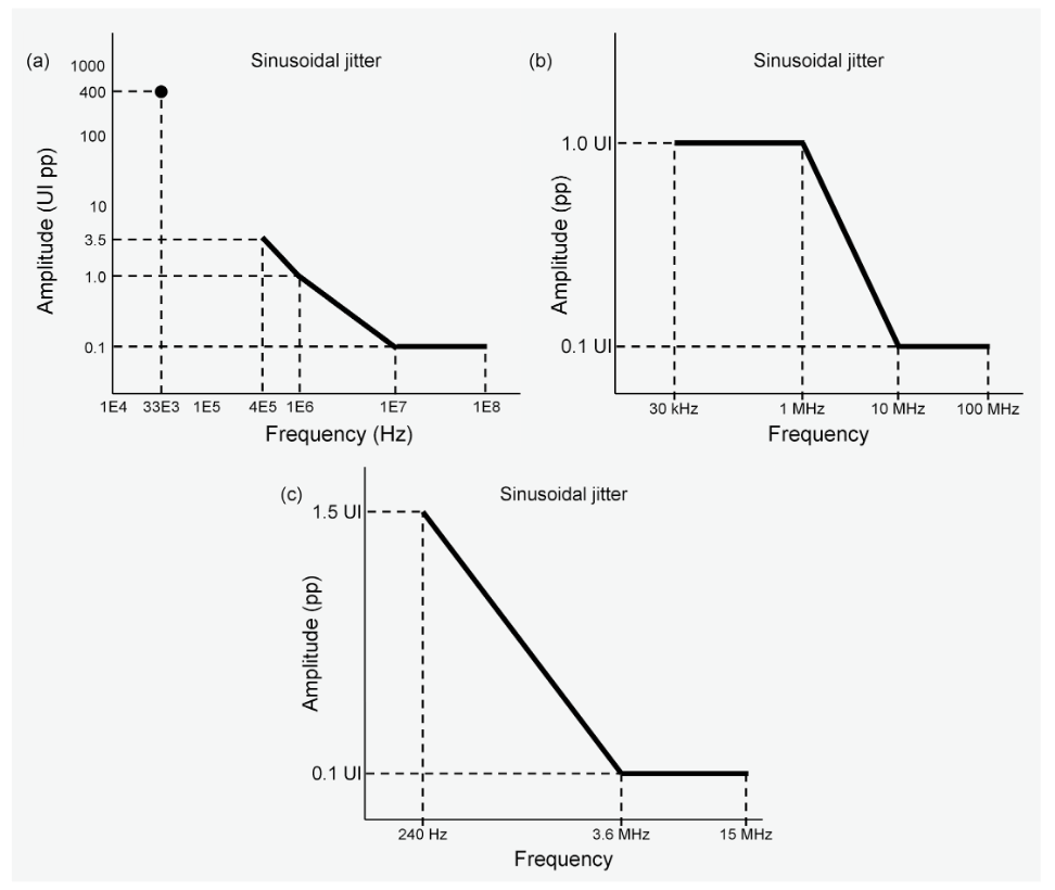
The tests vary for different standards but follow the same theme: begin with low frequency, high amplitude SJ and measure BER across an SJ template like one of those shown in Figure 12. If the receiver performs at or better than the required BER across the SJ template, then it is compliant.
In practice, the test is usually performed at a handful of points in the SJ template; at least one point at low SJ frequency and high amplitude, one point within the CR roll off, and one at high SJ frequency, low amplitude.
7. Conclusion
The rapid expansion of I/O demands in every type of enterprise computing from data centers to business-wide servers is pushing high speed connectivity standards like PCIe and SAS to higher data rates and, with every increase in data rate, receiver testing grows more complicated. The greatest complications for Gen4 are link training, the use of models to calibrate the stressed eye parameters, and the introduction of FEC.
The BERT's roles as the ultimate judge of component and system performance and as stressed signal transmitter are well established. We've seen here that well equipped BERTs can also play key roles in diagnostic test and debug.
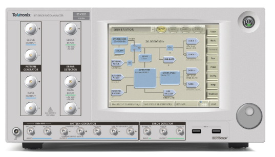
The protocol-aware BSX-series BERTScopes with Error Location Analysis and built-in 4-tap transmitter FFE, can:
- Test adaptive equalization link training.
- Transmit scrambled and encoded signals with symbols packaged in protocol blocks and, at the error detector, decode and descramble patterns and match block payloads.
- Create stimulus-response test conditions with sequence advance by software control, external signal, or by matching detected patterns with up to 128 states and two levels of loop nesting.
- Simultaneously measure both pre-FEC and post-FEC BER.
- Perform stressed receiver tolerance tests with the complete suite of precise signal impairments including DM-SI and CM-SI.
- Process data in real time at up to 32 Gb/s.
- Provide actionable diagnostic information.
We can't probe within the serdes chipset to analyze the performance of its differential input, clock recovery, equalization, and bit slicer, but the BSX-series BERTScope's large pattern memory and Error Location Analysis allows us to diagnose the performance of each internal component with carefully chosen test pattern-stress combinations.

