Silicon Carbide (SiC) MOSFETs are increasingly being used in industries ranging from electric vehicles and solar power, to backup power systems. This is thanks to their ability to withstand high temperatures, offer faster switching, deliver higher efficiency especially at higher voltages, and high current capacity.
However, there are some challenges in validating designs using SiC MOSFET’s. The switching characteristics that make them attractive also pose challenges for accurate validation measurements. The right probe selection and application can greatly improve measurement accuracy.
After reading this post, you can find more detailed information in a new Tektronix application note titled Effective Measurement of Signals in Silicon Carbide (SiC) Power Electronics Systems.
What is a SiC MOSFET?
A Silicon Carbide MOSFET is a specific type of MOSFET designed with silicon carbide. They are characterized by their exceptional energy efficiency, excellent heat dissipation, high current density, outstanding high-temperature performance, and superior voltage rating. But, to understand SiC MOSFETs better, you need to first understand what a MOSFET is and the types of applications involved.
Introduction to MOSFETs
A MOSFET, or Metal Oxide Semiconductor Field-Effect Transistor, is a type of transistor used for amplifying or switching electronic signals. The MOSFET is a core component in modern electronics and is the building block of most of the world’s integrated circuits. Over time, technology has transitioned from the use of silicon to silicon carbide, or SiC, in the development of MOSFETs. This progression has led to significant improvements in efficiency and performance.
Applications of MOSFETs
MOSFETs, particularly power transistors, are used in a wide range of electronic applications. They are integral to power supplies, electric vehicle control systems, and sustainable power applications such as solar, wind, and thermal energy systems. Furthermore, MOSFETs play a crucial role in radio systems, where they are used in audio amplifiers to modulate the output of the radio signal.
Advantages of a SiC MOSFET: Reliability and Performance
Silicon Carbide (SiC) MOSFETs have a proven track record of high performance and reliability. They are extensively used in various applications including electric vehicle battery chargers, photovoltaic (PV) inverters, high voltage DC/DC converters, and renewable energy systems. The use of silicon carbide in SiC MOSFETs provides significant benefits in terms of performance and size, making them a preferred choice for a wide range of electronic applications.
Tektronix oscilloscopes are well suited for MOSFET design and testing, providing a variety of tools and solutions to measure the performance of SiC MOSFETs.
Challenges When Measuring SiC MOSFETs in Power Electronics Systems
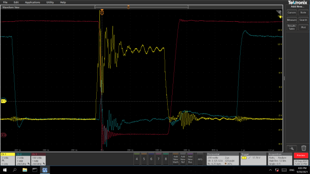
The challenges you will face when measuring SiC MOSFETs will depend on where and how you’re measuring. Especially in high-side switches, the gate voltage signal on high side (VGS) is floating on a high, rapidly switching offset voltage. These “common mode” variations can cause ringing in the measurement system, as shown in the figure above, and it can be impossible to determine if the ringing is coming from the DUT or from the measurement system. The drain-to-source voltage (VDS) is significantly higher than VGS and is often floating with respect to earth ground. Drain current measurements also require care to insure adequate oscilloscope and probe bandwidth for accurate measurements.
Accurate Silicon Carbide Gate Voltage Measurement
Gate-to-source voltage (VGS) measurements, especially on high-side switches, can be especially challenging. The gate threshold voltage is usually just a few volts, so it is relatively small compared to VDS which can be hundreds of volts.
Traditionally these measurements have been performed using differential probes like the Tektronix THDP0200 Differential Probe. However, using a differential probe may lead to unnecessarily large design margins, especially when making high-side VGS measurements. The voltage on the source terminal of the high-side MOSFET is changing quickly, relative to earth ground. Making this measurement accurately requires very high common mode rejection ratio (CMRR) at high frequencies. Ringing introduced by differential probes can result in devices that are within specification seeming like they are not. Adjusting your design to slow down switching and eliminate spurious ringing will “undo” some of the benefit of designing with these high-speed SiC MOSFETs.
Having a probe with a high CMRR limits the effects of common mode voltage on the output. To enable more accurate measurements, it is recommended that you use optically isolated probes like the IsoVu optically isolated probes. These probes reject 80 dB of common mode signal at 1 GHz and 120 dB at 100 MHz. An example of this effect is shown in Figures 1 & 2 below.
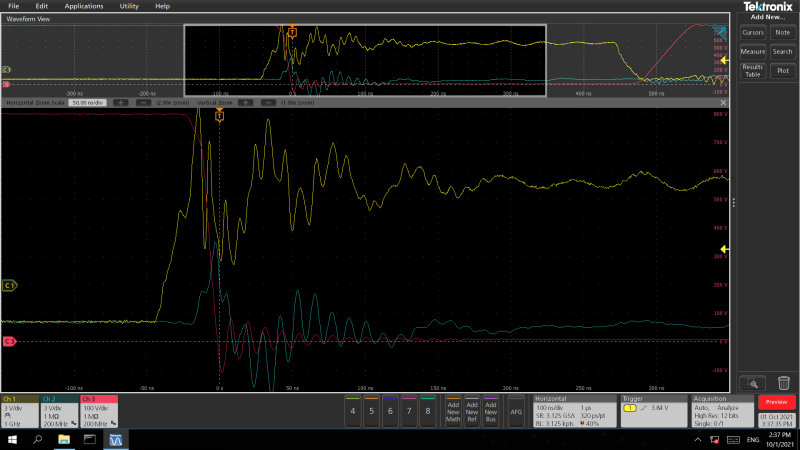
Figure 1. Gate voltage signals observed using a passive probe on the low side (yellow trace) and differential probe on the high side (blue trace). This setup shows significant ringing on the VGS signals, including the high-side drive signal.
Figure 2. Gate voltage signal observed using two IsoVu optically isolated probes (yellow & blue traces). The ringing is greatly reduced, and detail can be seen on the low-side gate signal (yellow). High common mode rejection eliminates the spurious disturbances on the high-side gate signal (blue).
Accurate Silicon Carbide Drain Voltage Measurement
To measure drain voltage in SiC MOSFET’s, you can either use ground-referenced passive probes or differential probes. Ground-referenced probes are relatively inexpensive and are included with oscilloscopes, but they should only be used for ground-referenced measurements. Connecting a ground-referenced probe to a floating (ungrounded) component will result in current flow in the ground lead. And when using multiple ground-referenced probes, extreme care must be taken to connect all reference leads to the same earth potential. An example of an easy mistake using two probes is given in the Effective Measurement of SiC Application Note.
Never remove the ground pin on the power cord of your oscilloscope because this allows the chassis of the scope to float. This presents a safety hazard and may negatively impact measurement performance.
If you do have a ground point available in your design, Tektronix TPP0850 passive high-voltage probes are a good choice for drain voltage measurements on SiC devices. These passive probes can handle up to 1000 Vrms and 2.5 kV peak and present only 1.8 pF of loading.
Using a differential probe such as a Tektronix THDP0200 Differential Probe within its specifications is a simpler and safer way of taking drain voltage measurements. Since it is decoupled from the ground, it provides better safety for both the measuring units and the operator.
For more information, and to learn how to make accurate current measurements using a Rogowski coil, download the full application note, Effective Measurement of Signals in Silicon Carbide (SiC) Power Electronics Systems, which has greater detail and shows measurements on a Wolfspeed CAB011Ml2FM3 high performance, half-bridge module. It also includes a section on making accurate current measurements using a Rogowski Coil or CVRs, and how to perform low-impact connections from a probe to your MOSFET device under test.