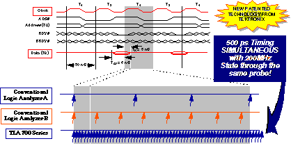
Tektronix' asynchronous digital oversampling architecture enables timing verification simultaneously with state analysis through the same probes
In the fast-paced world of microprocessor design, hardware designers need to do their jobs better but on shorter schedules. So it is imperative that they have effective tools that give them a clear view into all the detail of their most demanding designs. That means, designers need a logic analyzer with superior timing resolution across hundreds of channels.
After in-depth marketing research to determine designers' needs, Tektronix adapted an innovative asynchronous oversampling architecture used originally in their oscilloscopes to successfully create a new breed of logic analyzer-the TLA 700 Series-that delivers sub-nanosecond sampling resolution across all channels (see sidebar). This asynchronous digital oversampling not only improves troubleshooting, but more importantly, it opens up a whole new area of measurement capability for logic analyzers-comprehensive timing verification.
In fact, the TLA 700 Series produces enough detailed timing information to support detailed timing verification simultaneously with state analysis, on each and every channel without having to re-probe or use expensive, specialized timing modules.
Improved Troubleshooting
The TLA 700 Series and its remarkable resolution greatly streamlines the troubleshooting process. With MagniVuTM, the TLA 700 Series can acquire asynchronous and synchronous data simultaneously for each and every acquisition. So even if a state acquisition is specified, the designer can still view the asynchronous acquisition at any time, without having to re-acquire. That means when a problem occurs, the designer can immediately zoom in and examine the detailed behavior of all the signals with 500 ps resolution.
Finding subtle timing problems-glitches, delays or noise-is now a straightforward process with 500 ps resolution on all channels. Other logic analyzers simply do not have enough timing resolution across all their channels to fully characterize the timing performance of a microprocessor-based design. The only option is to hook up a second set of probes attached to special, high-speed timing analyzer modules. But then the channel count is severely limited, perhaps as low as 16, and the double probe loading severely distorts high-speed signals. Hooking up a second set of probes is so tedious a task that it is rarely undertaken. Or the designer uses an oscilloscope and laboriously probes pins one by one, carefully correlating the data signals with the clock to which they are referenced.
Now designers can hunt for the root causes of problems in detail across all the channels right when they occur. This is especially useful for troublesome anomalies that occur infrequently. For example, the processor reads a value that is invalid and causes the application to fail. After triggering the logic analyzer on the faulty read cycle, the designer can use MagniVuTM to see the detailed timing of every signal around the critical event that triggered the current acquisition.
Until now, finding glitches has been a cumbersome process. But thanks to asynchronous digital oversampling, the TLA 700 Series can automatically hunt for glitches on every channel with sub-nanosecond resolution. The glitch detector monitors the high-speed data stream out of the sampler (figure 1). When a glitch occurs, the detector triggers the analyzer. The designer then can use MagniVuTM to actually see the number, width, and placement of glitches within the sample period with 500 ps resolution.

Moreover, the TLA 700 Series can directly trigger on violations of the most crucial synchronous timing parameters-setup and hold time. The setup and hold checker detects transitions in the input signals after they are acquired with the high-speed digital sampler. The transitions are then skew adjusted and violations are flagged if the transitions are within the interval defined by the user.
Comprehensive Timing Verification
The benefits of asynchronous digital oversampling don't stop with improved troubleshooting and state analysis. With 500 ps resolution, the TLA 700 Series is equipped to perform full-fledged timing analysis.
Asynchronous digital oversampling also enables the TLA 700 Series to produce extremely precise time stamps-an important feature for characterizing clock stability. Time stamps values are derived by identifying the precise placement of the clock edge in the oversampled data stream of the specified clock signal. The result is exceptional 500 ps resolution stamping that is a remarkable improvement over other logic analyzers.
The expanded capabilities of the TLA dramatically streamline the entire hardware verification process for the designer. Instead of using several instruments and having to struggle with multiple sets of probes, they simply attach the TLA. Now designers can directly verify the design against detailed timing simulations, viewing the timing of clocks, data and address signals with respect to each other and asynchronous inputs.
- Clock Performance: In high-speed logic design, clock distribution and signal quality are foremost concerns. With the TLA 700 Series connected, designers can easily acquire the clock signals at each critical distribution point and see the effects of their clock distribution implementation. They can view these effects with MagniVuTM, examine clock stability using the 500 ps timestamping or track down glitches in the clock lines with the glitch detector. In addition, this resolution supplies sufficient detail for characterizing signal parameters, such as clock pulse width and duty cycle, anywhere in the system.
- Data Bus Timing: The designer can exhaustively examine the performance of a system's entire data bus with the TLA 700 Series. First, setup and hold violations can be pinpointed with the setup and hold checker and examined with MagniVuTM. Even the margins for setup and hold can be characterized, to the give the designer an idea of how well the circuitry will accommodate component and temperature variations. Moreover, timing of the data bus relative to all the different memory and attached peripheral devices can be verified.
For example, the TLA 700 Series could trigger on a series of reads and writes to SRAM, DRAM, ROM, and peripherals. The timing information around each of these accesses could then be examined and characterized. For each type of bus access acquired, the designer can instantly zoom in with MagniVuTM without having to re-acquire or bother with attaching a second instrument.
- Address Characterization: Address timing is an important element of system timing that is easily overlooked. If address values become valid later than expected, the memory devices or peripherals may not have sufficient address setup time. Also, many embedded system designs utilize asynchronous memory or peripherals where the delayed settling of addresses results in late delivery of data, potentially causing problems at the other end of the bus cycle. This can be especially complex when more than one device can drive the address bus, for instance when a DMA controller or a second processor is used. In newer microprocessor designs, the address is often pipelined-where a new address for the next access appears before the data for the first address is available. So it is important that the designer be able to carefully examine the interaction between address, data and control lines.
Besides providing detailed address timing information, the TLA 700 Series incorporates a proven Tektronix technology for clocking microprocessor bus activity. Called the Clocking State Machine, this 200 MHz synchronous state machine can monitor up to twelve clock and control lines and identify the precise point at which to sample Address, Data and Control signal information. Each kind of information is sampled when valid and held until the bus cycle is complete. Then, the entire bus cycle is stored as a single synchronous transaction with a timestamp indicating the precise time at which the cycle was completed.
- Asynchronous Inputs: The TLA 700 Series can also trigger on asynchronous inputs-such as interrupts, signals related to wait lines-READY, DTAC, DSACK, etc.-and measure the timing of the specified channels with reference to the system clock. This makes it easy to verify the timing of asynchronous inputs against microprocessor specifications.
- Relating Timing Problems to Software Execution: Sometimes, a timing problem can have a direct relationship to software execution. Occasionally, timing-related problems only occur when a certain combination of hardware or software events coincide. With the TLA 700 Series the designer can trigger on these combinations of hardware and software events and view the timing that caused them. This is extremely useful where the timing of a section of hardware is affected by the operation of other hardware which in turn is controlled by software-a complicated scenario that is not unusual in embedded applications.
There are also times when tracing a problem requires exclusively monitoring accesses to a specific memory address or peripheral device and storing large quantities of those accesses in order to find the one related to the problem. In addition to storing the individual accesses, the TLA Series can store a block of bus cycles around each access-31 cycles before and 31 cycles after each access. This enables the designer to view the software context to see precisely which software function caused each access.
New Era for Logic Analysis
Asynchronous digital oversampling greatly expands the importance of logic analyzers in debug and verification of microprocessor-based designs. With sub-nanosecond resolution across all channels coupled with substantial memory resources, the logic analyzer can efficiently track down the most insidious problems. Then, without having to move a probe or hook up another instrument, the designer can perform comprehensive timing verification for the entire design. Even on the most aggressive schedules, designers now have the ability to efficiently debug and verify their most complex, microprocessor-based designs.
Sidebar: The Power of Oversampling
Asynchronous digital oversampling serves as the cornerstone of the TLA 700 Series. Inside this logic analyzer, a high-speed digital sampler continuously samples at 500 ps intervals for each channel. This extremely high resolution produces an incredible two gigabits of sample data per second on each channel of the logic analyzer. Eight bits of data at a time from the sampler are loaded in parallel every 4 ns into a shift register that feeds out selected pieces of the data to a 512k memory based on user-defined triggering and storage settings. As a result, more samples are acquired than are used for state analysis-hence the term oversampling. This large memory stores asynchronously acquired data at up to 250 MS/s or synchronously acquired state data at up to 200 MS/s for each channel.
As the overall state activity is stored in the larger memory, complete timing information is simultaneously captured in a smaller, faster on-chip memory for every channel. All data from the sampler is directly written into the high-speed memory which is also in a circular buffer format. This 2k deep memory is large enough to store 1 µs worth of data for each channel-or eight to 20 cycles of information for today's leading processors-with 500 ps resolution (figure 3). Called MagniVuTM, this faster memory gives the designer a window into the actual signal activity for each and every channel-up to 136 per module and 680 per instrument-and for each and every acquisition.

These two memories together ensure that the TLA 700 Series gathers a complete picture of signal activity during state analysis, providing simultaneous 2 GHz timing and 200 MHz state analysis. And no reprobing is required to view high-speed data alongside state information. The designer only needs to attach one set of probes to view all activity (figure 4).

