Abstract
The electrical compliance test specification drafted by PCISIG requires testing loop response of the Phase Locked Loop (PLL) used in add-in cards to generate a local transmitter clock from a 100 MHz reference oscillator. There are several possible methods for performing this test. This paper provides an overview of the significant ones, including one method based on an instrumentation-quality clock recovery instrument. The clock recovery method is a single-instrument solution that provides superior test accuracy, resolution, and throughput at minimal cost. The measurement output results are displayed directly without the need for interpretation, minimizing chances for operator error.
The transmit clock on PCIe add-in cards is generated on each board by multiplying a 100 MHz reference clock using a phase locked loop. The 100 MHz reference clock is distributed by the motherboard to all cards. To control jitter rejection performance in the system, the PCIe 2.0 Specification stipulates the operating loop response characteristics of the onboard PLL; in particular, the minimum and maximum PLL loop bandwidth and peaking. Table 1, above, lists these PLL response characteristics as stated in the specification.

There are several methods of measuring PLL loop response, based on the type of test instrumentation used. As expected, the various methods trade off test accuracy, test speed (throughput), ease of use, ease of setup, and initial cost. In addition, some methods have limitations preventing their universal use on all types of PLLs. While all methods can test compliance to the specification requirements, some offer additional information useful to the clock designer for optimizing a design.
For consistency and repeatability, all methods are assumed to employ the use of the SIG-supplied standard test fixture, the Compliance Base Board (CBB), version 2.0.
An overview of the basic test methods available follows.
Spectrum Analyzer Method
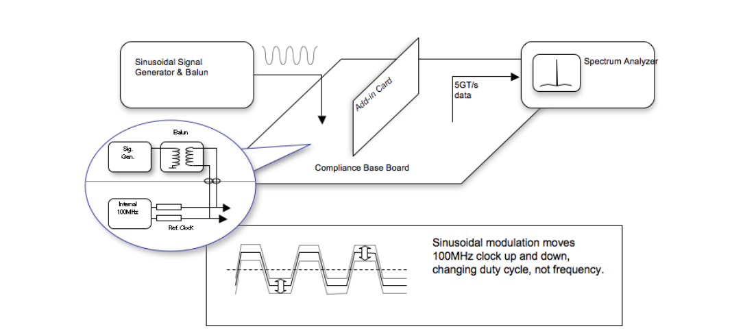
The Spectrum Analyzer-based measurement is the traditional method of characterizing loop response of PLLs. Two instruments are employed; a sinusoidal signal generator with sweeping ability, and a spectrum analyzer. The signal generator is used to modulate the reference clock duty cycle, and the transmit clock output is measured at one of the data lanes with the spectrum analyzer. Since it is not practical to synchronize the signal generator to track the local oscillator of the spectrum analyzer, the measurement is made by plotting an envelope of the peak amplitude measured, using the ‘peak hold’ function available in most spectrum analyzers. The oscillator sweeps continuously, much faster than the sweep rate of the spectrum analyzer.
The output spectrum displays a peak and the data rate fundamental and all harmonics, with the sideband slope being a plot of the PLL band-width. The output of the analyzer is not scaled as an absolute value. Rather, a relative measurement is made by using either paired delta cursors (if available), or manually with a single cursor by recording the absolute nominal and peak values and subtracting the test limit from it.
The method used to modulate the reference frequency has impact on the universal applicability of this test method. In this test approach, the solder-in jumpers on the CBB are configured to sum a differential test signal with the 100 MHz oscillator generated on the CBB itself. An external BALUN is placed between the signal generator and the summing point on the board to modulate both halves of the differential clock pair. The result is an amplitude-modulated clock signal, where the crossing point is essentially moved from center of the differential signal by the external sine source. Because the crossing point is altered, and not the frequency of the 100 MHz reference oscillator, this method actually modulates the duty cycle of the PLL reference. This will appear as phase modulation to a single-edge phase detector and therefore works in this case. However, to reduce jitter when moving up to 5 GT/s designs, many designers will opt to lower multiplying ratio by employing PLL designs that compare phase on both rising and falling edges. These types of PLLs only track the total period of the clock and will not respond to duty cycle variations. Therefore, they cannot be characterized using this method of reference modulation.
Because the phase modulation of the PLL reference is generated by amplitude-modulating the 100 MHz reference clock, the side bands on the spectrum analyzer contain both AM and FM components. Care must be taken when interpreting the results to assure the measurement reflects only the PLL bandwidth.
As with all measurements made with a swept heterodyne spectrum analyzer, there is a direct tradeoff between bandwidth resolution and sweep time. Because the test limits range down to single-digit MHz, a relatively low frequency resolution bandwidth is required — typically 30 kHz.
The detectors in heterodyning spectrum analyzers measure magnitude only, so phase information of the loop response is not available. While phase is not required for testing compliance to the base specification, it can be used by the clock designer to determine the PLL phase margin — an extremely powerful tool for evaluating the design.
The spectrum analyzer-based approach provides a wide dynamic range of amplitude, which simplifies the test setup. The amplitude resolution is limited to a practical value of about 1 dB or slightly better, which is marginal when testing bandwidths at peaking values of only 1 dB.
The test setup is somewhat complicated, requiring setting operating parameters of the signal generator and measurement parameters of the spectrum analyzer. Care must be used in setting the signal generator amplitude to avoid overdriving the summing node on the CBB. Pre-stored setups could be used to simplify this; however the resulting plot still requires some interpretation and manual cursor scanning to read the parameter values.
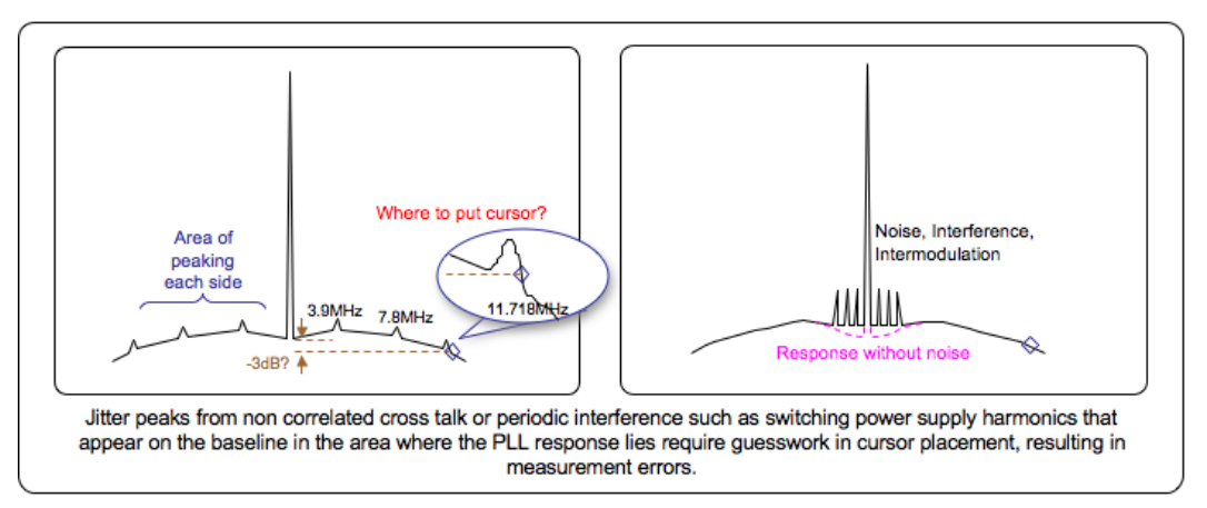
The manual cursor placement is often a source of errors and non-repeatability in the measurement. In some cases, the DUT has jitter spectral components which are not related to the clock data rate, such as switching power supply harmonics for example. These peaks can occur in the baseline area where the PLL response is being measured, precluding the ability to place the measurement cursor on the actual trace, requiring the user to guess the location if the peak were not there.
Oscilloscope Method
Oscilloscope-based methods replace the spectrum analyzer with a digital oscilloscope. The most straight-forward method is to use the FFT capability of the scope to generate the frequency domain information. This method offers several improvements over the spectrum analyzer. The frequency resolution is a function of the sampling rate and the memory length, and can be optimized for the measurement requirements. The signal acquisition and measurement throughput is much faster than the slow-swept local oscillator in the spectrum analyzer. While the dynamic range is an order of magnitude smaller, requiring the oscilloscope to set the proper scale factor before measurement, the resolution is better than the spectrum analyzer. However, the dynamic frequency response accuracy of the best oscilloscopes is on the order of +/– 1 dB, limiting the measurement accuracy to about 1 dB. The vertical scaling is intrinsically linear, requiring parameter math operations to convert to dB.
Unlike the spectrum analyzer, the FFT calculation in the oscilloscope can generate phase response as well as magnitude.
The oscilloscope-based method uses the same signal generator configuration as is used with the spectrum analyzer method, and therefore shares the need for additional instruments and the same inability to be used with PLLs that employ dual edge phase detectors.
Bit Error Rate Tester (BERT) Method
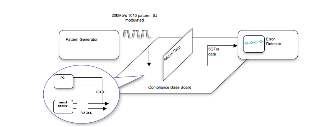
A high performance Bit Error Rate Tester (BERT) can be configured to directly measure PLL loop response. A BERT has both stimulus and measurement capability, which allows this test to be performed with a single instrument. For PLL measurements, the BERT must have the ability to inject “stress” (calibrated jitter) into the pattern generator 100 MHz differential output with correct DC offsets.
The BERT-based measurement uses a different approach to stimulating the PLL under test than that used by the spectrum analyzer and oscilloscope methods. Rather than summing a distorting signal into the 100 MHz reference oscillator generated on the compliance base board, the BERT provides the reference signal by programming the pattern generator to output a 1010 pattern (clock) at a 200 Mbps rate. This equates to a 100 MHz differential clock. The stress generator is set to inject sinusoidal jitter into the pattern output, which phase-modulates the period of the waveform. This configuration requires the resistor/jumpers on the CBB to be set for external reference clock input.
The pass-through jitter in the output of the PLL under test is measured by the BERT Error Detector. By stepping the frequency of the sinusoidal jitter stress, a plot of jitter transfer function can be generated. Additional math processing produces a plot of the PLL loop response.
As with the oscilloscope-based approach, it is possible to perform this measurement manually. However, a ‘canned’ software option automates the task, minimizing the potential for user error while speeding up the measurement and providing a direct pass/fail test.
The BERT-based measurement provides higher accuracy and repeatability than either the spectrum analyzer or oscilloscope can offer. With automated software, the measurement is extremely fast – just a few seconds.
Clock Recovery Instrument Method
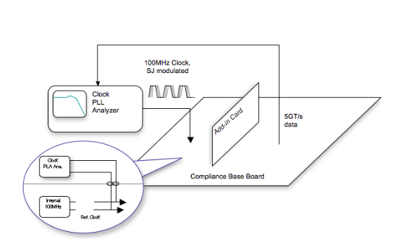
A high performance Clock Recovery Instrument can be configured to measure PLL loop response, offering several advantages over the other methods previously discussed. These are essentially ‘instrumentation grade’ clock recovery units, which use a sophisticated PLL design to operate over a wide range of clock frequencies, with calibrated and userprogrammable loop response. To facilitate self-calibration, these instruments contain a direct digital synthesizer (DDS) to produce various signals. The output of the DDS is made available externally in the PLL test configuration, where it serves as the reference clock. As with the BERT-based test method, the clock recovery instrument method only requires a single instrument for generating the stimulus and measuring the output. However, the DDS source clock recovery instrument-based method differs from the Spectrum Analyzer and Oscilloscope approaches in the fact that the reference signal is programmed to maintain a perfect 50% duty cycle. This allows universal testing of all PLL topologies, including those with dual edge phase detectors. The capability to maintain a 50% duty cycle while modulating the reference phase is a unique built-in feature of either the BERT or clock recovery-based test methods.
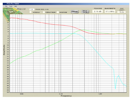
The output signal from the user-selected lane on the Compliance Base Board is routed to the data input connectors of the clock recovery instrument. From there, the clock is recovered with the instrument’s precision PLL. The output of the phase error detector is digitized and processed to determine the relative phase error. The sine and cosine information from the digitized waveform is used to compute the phase and magnitude of the phase modulation passing through the PLL under test versus frequency. Because the phase error measurement is synchronized to the modulation of the reference clock, the measurement can be correlated to greatly enhance the dynamic range — to more than 75 dB.
In addition to maintaining a 50% duty factor while modulating the phase of the test signal, the clock recoverybased approach offers several advantages over the other approaches. While maintaining a dynamic range beyond that provided by spectrum analyzers, an amplitude resolution of 0.01 dB is possible, which provides the highest accuracy and repeatability of the measurements. The frequency resolution is also high, without compromising rapid test time. A complete measurement can be generated in less than 10 seconds. The measurement method inherently produces a phase plot as well as magnitude. While only the frequency at the –3 dB point and peaking level are required to verify compliance, the addition of a phase plot allows the user to determine the phase margin of their PLL design – an extremely powerful tool for evaluating a design. Finally, this approach can also generate the PLL gain (some times called jitter transfer function, JTF) plot.
Besides the Compliance Base Board, which is required for all testing, the only additional accessory required with the Clock Recovery-based method is the set of four interconnecting cables.
Summary
All four methods can perform the required PLL loop response measurements required in the PCIe 2.0 base specification; however, only a phase modulation method shared by the clock recovery and BERT-based approaches will work with all PLL designs. The methods differ considerably in the complexity of setup and results interpretation, resolution and accuracy, repeatability, and initial cost. The clock recoverybased approach is a single-instrument solution that provides high accuracy, high resolution, and repeatability, with the simplest setup and the lowest cost. It also has the advantage of providing additional information that enables the PLL designer to better understand the performance of their design.

