Semiconductor characterization labs, technology development labs, modeling labs, and reliability labs often require several different source and measurement instruments as well as connections to multiple devices. Switching ensures that test connections, and thus measurements, are made with a high degree of repeatability. The potential for a variety of connections between the device pins and instrumentation makes the matrix an appropriate switch configuration, as illustrated in Figure 1.
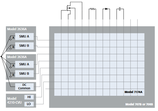
Today's semiconductor devices have more stringent requirements targeting more ideal device behaviors, for example, requiring lower leakage when the device is off. Small variations in device leakage currents can signal manufacturing defects and reliability issues. These device requirements propagate to the switch system requirements.
Although most semiconductor applications require sensitivity, it is rarely required for every measurement. Low current measurements require longer settling times, but it's undesirable to impose that time burden for measurements on all devices. This is especially critical for process control monitoring applications, where testing must be done quickly to tweak manufacturing processes and minimize product waste.
Keithley has decades of experience in providing switching solutions to semiconductor manufacturers worldwide. The latest large-format switch mainframes, the Models 707B and 708B, continue this tradition with new digital and user interface designs that deliver higher switching speed and greater ease of use, without interfering with the low current sensitivity of the switch matrix cards. This note discusses how to design a semiconductor switch system that will take maximum advantage of these mainframe capabilities.
Switch System Configuration
Selecting the correct switch matrix card to route the signals of interest is critical to attaining the desired measurement accuracy and resolution. The cost of a sub-picoamp measurement instrument and a 10MHz C-V meter is wasted if those signals are being routed through a switch with an offset current specification of 1nA and 100kHz bandwidth. The impact of the switch card must be taken into consideration for both AC and DC measurements.
DC Characterization
For low current measurement, select a switch card with an offset current that's lower than the anticipated measurement. The offset current is a noise current on the card that exists even when no external signals are being routed. This noise current is the result of the switch card's design and cannot be eliminated.
Leakage currents are additional noise sources that result from voltage drops across insulators in the test system. Leakage currents can vary with applied voltage. Use a guarded switch to minimize leakage currents and improve overall response time. Guarding reduces leakage currents by routing these currents away from the high impedance terminal where low current measurements are made. The guard terminal is a low impedance terminal that is at the same potential as the high impedance terminal. Therefore, the guard terminal eliminates the potential drop across the insulator, which reduces the leakage current to near 0 pA. Guarding also eliminates the need to wait for the cable capacitance to charge because the voltage drop across the cable capacitance remains near 0V. Note the example in Figure 2.
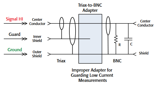
To minimize settling times and leakage currents, carry the guard from the measurement instrument all the way to the device pins. Almost all Keithley SourceMeter® instruments include a driven guard terminal, as shown in Figure 2. Given that guard is at the same potential as the Output HI terminal, triax cabling is required for user safety whenever the maximum output voltage exceeds 42VDC. As shown in Figure 3, converting to coaxial cable by dropping the inner shield of the triax connector eliminates the benefits that guarding offers. To ensure triax cabling is used, Keithley's semiconductor matrix cards engineered for low current switching are supplied with triax connectors.
Note: Capacitance of second insulator is irrelevant when circuit is floating.

Consider the isolation specifications of the switch when switching signals to high impedance devices. Both path isolation and signal-to-chassis isolation must be higher than the resistance of the device under test to avoid measuring the switch card characteristics rather than the desired device characteristics.
Models 707B and 708B Semiconductor Switch Matrix Mainframes support Keithley switch cards with proven low current performance in semiconductor research and process control monitoring environments.
The Model 7174A matrix card is often considered an industry standard, combining low offset current, high isolation and wide bandwidth. It incorporates isolation relays at every crosspoint so that the rest of the matrix (other unused crosspoints on that row and column) is isolated from the path in use. This configuration permits offset current ≤100fA max. with typical performance of 10fA along a single pathway. Reed relays provide contact life of 100 million cycles under the recommended cold switching operation.
Although the Model 7072 and Model 7072-HV matrix cards don't offer the same offset current and bandwidth specifications as the Model 7174A, these cards are suitable for a variety of tests, especially those requiring low current sensitivity on only a few measurement terminals. Two rows are optimized for low leakage measurements with <1pA offset current. These same rows on the Model 7072-HV card also support signals up to 1300VDC, making it suitable for breakdown measurements. Column isolators isolate these rows from four general-purpose rows located in the center of the card, which are intended for tests that don’t require low current sensitivity, such as on-state characterization of FETs.
AC Characterization
Transient and AC characterization are very important in the semiconductor industry for developing suitable electrical models and understanding state transitions in the device. AC characterization requires consideration of the path isolation and bandwidth specifications of the switch card.
To simplify capacitance-voltage (C-V) measurements, note the capacitive component of the path isolation specification and select a switch with low stray capacitance. However, most C-V meters, such as Keithley's Model 4210-CVU, include offset correction routines to cancel out the value of the stray capacitance from the measurement. For the best measurement accuracy, it may be necessary to compensate each possible C-V measurement path through the switch.
The bandwidth of the switch card must support the highest test frequency of C-V measurements in the system. Using a switch card with lower bandwidth attenuates the AC voltage sourced from the LCZ meter and produces incorrect results. As the bandwidth is usually specified at the frequency at which the signal is attenuated by 3dB, it is a good idea to select a bandwidth that is higher than the test frequency.
Switch card bandwidth is also important for pulsed device characterization. The bandwidth may be related to the rise time using this formula:
Bandwidth
If the bandwidth of the card is 10MHz, this means that an ideal pulse with 0ns rise time would be degraded to one with a rise time of 35ns at the output of the switch. The total rise time of the pulse at the output of the switch matrix is the root sum of squares of the rise time of the input signal, cables, and switch system. Therefore, to minimize pulse degradation, it is a good rule of thumb to choose a switch with a rise time that is three to five times faster than the signal rise time. For example, if the rise time of the signal of interest is 1ms, then the rise time of the switch should be 240-300ns or faster to ensure minimal degradation.
High frequency applications are best addressed using the Model 7173-50 High Frequency Matrix card, which has 200MHz bandwidth. This results in a rise time of less than 2ns, making it an ideal solution for switching pulsed signals. Its coaxial connections allow quick and simple connections to many pulse generators and LCZ meters.
The bandwidth and path capacitance specifications of the Model 7174A make this card suitable for C-V and low frequency pulsed I-V measurements. Its path isolation capacitance of approximately 1pF and 30MHz bandwidth accommodates most C-V instruments. The switch has a rise time of less than 20ns, making it suitable to carry pulsed signals with rise times of approximately 60ns or more.
In addition to two low current rows, both Models 7072 and 7072-HV Matrix Cards feature two rows optimized for C-V measurements. These rows have 5MHz bandwidth. Additionally, relays on each column isolate the C-V rows from the other rows of the card. This results in a stray capacitance of 0.6 pF.
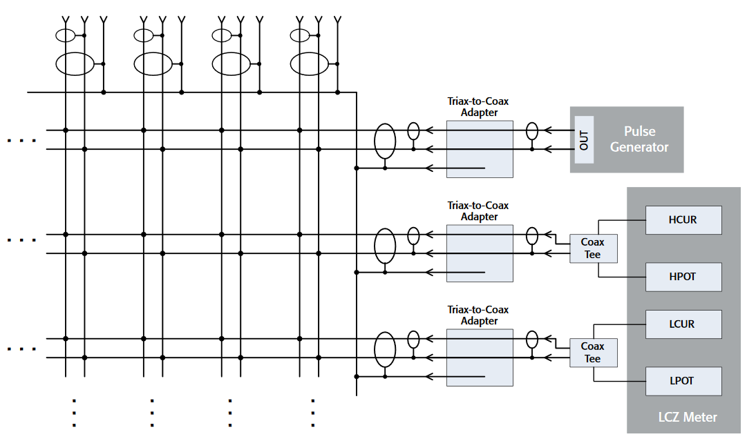
When converting a coaxial connection from a pulse generator or LCZ meter to the triaxial connection on a switch card, take care to select appropriate adapters to protect signal integrity. The coaxial shield should be carried surrounding the signal conductor up to a point very close to the device. Tie (or short) the shields of all cables from the pulse generator or LCZ meter together as close as possible to the device. Be aware that the outer shields of all triax connectors on the switch card are often tied together and grounded. Therefore, the outer shell of the triax does not serve as a good return path for AC measurements. Use triax-to-coax adapters, such as Keithley's Model 7078-TRX-BNC, which bring the center conductor and inner shield to the coaxial connector as shown in Figure 4.
Matrix Expansion
In many test cases, the number of devices and measurement instruments exceeds the size of the configuration a single switch card can offer. Models 707B and 708B incorporate an analog backplane to carry general-purpose signals, which allows extending the four general-purpose rows of the 7072 and 7072-HV cards easily to other cards. These cards connect to the backplane when inserted into the switch mainframe. For low current and high frequency signals, separate coaxial expansion cables are supplied with each matrix card to maintain high signal integrity. All four cards compatible with the Models 707B and 708B support the use of these coaxial expansion cables.
When expanding the switch system to use multiple cards, it is important to note that the specifications of the lowest performing card determine the minimum system specification. It is a good idea to use the same matrix card type when expanding a matrix.
Note, too, that high frequency signals undergo additional degradation when multiple cards are connected. For example, one Model 7173-50 switch card has a bandwidth of 200MHz; connecting three cards reduces the bandwidth to about 100MHz. Use a network analyzer to characterize the AC performance of the entire switch matrix before testing actual devices.
Switch System Timing
In semiconductor process control monitoring environments, maximizing the speed of test is just as critical as obtaining accurate results. Therefore, it is appropriate to consider the factors that affect switch system timing and identify some speed optimization techniques.
For high throughput applications, select a relay that both meets the application's electrical signal needs and actuates quickly. Reed relays, commonly used in precision low-level switching systems, are known for their high switch speed, high isolation, and long life. For reed relays, the relay actuation time begins when voltage is applied to the relay coil and ends when the contacts have closed and finished bouncing. In typical Break-Before-Make (BBM) relay closure operation, the actuation time is imposed each time the mainframe processes a command to close or open a relay. The mainframe waits for the actuation time to elapse before recognizing the relay as closed. Thus, the system timing for moving from one closed path to another includes the actuation time for two relays. The Models 707B and 708B allow users to configure the method in which relays close (Break-Before-Make or Make-Before Break) using the channel connection rule. One way to optimize switch system timing is to turn the channel connection rule “off” so that the switch mainframe attempts to open the first relay at the same time that it closes the second relay, potentially reducing the total time impact to a single relay actuation period. However, given that the order of closure and opening cannot be guaranteed when the channel connection rule is "off", users must implement cold switching.
To achieve ultra low level performance, it's essential to consider switch card settling. Several factors influence switch card settling after the relay actuation: (1) System capacitances that cannot be guarded out require time to charge to the test voltage and stabilize. (2) Although reed relays switch quickly in comparison with electromechanical relays, there may be mechanical movement or vibration in the contacts even after electrical contact is made and contact bouncing stops. This vibration may continue for another millisecond or so after the relay actuation time has elapsed. The vibration of the contacts in the presence of the magnetic field of the relay coil generates a noise current through the contacts. (3) Dielectric absorption of insulators and capacitances in the circuit allows these elements to retain or recover charge even after that charge is removed.
Switch settling is typically much longer than actuation time and affects the accuracy of the transmitted signal. As an example, the Model 7174A switch card has a specified relay actuation time of 1ms or less. This makes it 6-15 times faster than other switch cards for the Models 707B and 708B. However, achieving a noise floor of 400fA at an applied voltage of 10V with this card requires a settling time of 2.5 seconds and the addition of a delay after a voltage step. The settling time of any measurement path through the switch is determined by the time constants of all capacitances and dielectric absorption effects in that path. Characterize the total settling time by applying a voltage step at the system input and using a sensitive ammeter to measure the current decay over time at the output. Select a delay by observing the time at which the current falls below the expected noise floor for the device measurement.
The advantage of a fast-actuating relay can be negated by the digital speed of the switch controller. Take note of the switch mainframe’s timing specifications to process relay close and open operations and to respond to input triggers. Models 707B and 708B have modern digital engines with on-board processors to minimize mainframe overhead so that switch speed is largely determined by relay actuation time.
Let's examine the difference that higher command-to-connect speeds make by comparing the Model 707A with the Model 707B in the same test using the same set of commands.
In this example, the Models 707A and 707B are used to switch six diodes to the Model 2400 SourceMeter Instrument for a spot forward voltage measurement. The measurement time is minimized in order to show the effect of the mainframe overhead. The entire test sequence is looped 120 times for 720 measurements. Identical test code is used to control both switch mainframes. Table 1 compares the results. With the Model 707B, overall test time improved by more than 85% and mainframe overhead was reduced to less than 15% of the overall test time.
Table 1. Switch mainframe comparison using diode forward voltage measurement
| 707A | 707B | |
| Total Test Time (sec) | 82 | 10 |
| Measurement Time (sec) | 7.2 | 7.2 |
| Relay Actuation Time (sec) | 1.5 | 1.5 |
| Mainframe Overhead (sec) | ~73(~90% of total time) | 1.3(13% of total time) |
Unlike their predecessors, which required separate open and close commands for every path selection, the Models 707B and 708B offer a variety of commands that combine close and open operations to minimize communication traffic and command parsing and processing times:
- Close: Only closes specified relay without opening any other relay.
- Exclusive close: Opens all other relays of the mainframe and closes only the specified relay.
- Exclusive slot close: Opens all other relays on the same card and closes only the specified relay.
Take test sequencing into consideration to eliminate unnecessary relay closures and optimize throughput. For each switch path change, the switch system requires time to actuate relays and restabilize. Avoid wasting the throughput gains the switch system hardware makes possible by organizing the test sequence to minimize setup changes. Models 707B and 708B maintain state information and do not unnecessarily toggle relays that are already closed.
The Models 707B and 708B allow users the option of storing a relay sequence as a scan list. The mainframe can scan, that is, automatically cycle through the relay sequence, and close and open channels in response to a particular event or combination of events. Scanning is controlled by the instrument firmware. When a scan is defined, the switch mainframe reviews the relays to be actuated, performs checks on power requirements, and makes other preparations to optimize channel closures. These operations are normally done each time the switch mainframe processes a relay closure command. Scanning eliminates the need for a PC controller to send individual close/open commands for every path selection, thereby reducing software and communication overhead times, minimizing command processing time, and eliminating command parsing time. The use of scanning allows achieving the Models 707B's and 708B's maximum switch speed.
Built for Speed - Coordination with the Source and Measure Instrumentation
Of course, the semiconductor switch matrix mainframe is not the only factor that determines system throughput nor is it necessarily the dominant factor. It is good practice to first optimize measurement hardware since measurement times are significant when characterizing devices. However, to maximize overall throughput, good coordination between the semiconductor switch matrix mainframe and the source and measure instrumentation is essential.
Although delays to account for system settling (source settling, settling of low current measurement ranges, and charging of system capacitance) are necessary, beware of adding delays to account for operations on other test system hardware. Such delays are often longer than required because they must account for the variations in the timing of the other instrument. On occasion, such delays can be shorter than required and result in unexpected performance (switching before measurement is complete) or timeout errors. More precise timing can be achieved by using the built-in trigger functions. When triggering is configured, the switch can send a digital signal (output trigger) to other instruments to alert them to the completion of the relay action. Upon receiving the indication from the semiconductor switch matrix mainframe, the source and measurement instruments perform the configured I-V tests and generate output triggers upon test completion. The most efficient trigger models are interrupt driven and do not require the controlling computer to transmit alerts between switch and measurement instrumentation.
When multiple source and measurement instruments need to communicate with a single semiconductor switch matrix mainframe, a trigger controller may be required to logically sum or select the appropriate trigger signals to initiate an event. The trigger controller may be a separate stand-alone instrument or digital I/O card, or such capabilities may be built into the switch mainframe itself.
The Models 707B and 708B have built-in computer processing capability. Both can execute stored instructions, perform calculations, and wait for and generate digital trigger signals with response times on the order of microseconds, all with only minimal interaction with the controlling computer after initial configuration.
Similar capability is available with Keithley's Series 2600A System SourceMeter instruments. In fact, the analog performance of the Model 2636A complements the low current switch cards supported by the Models 707B and 708B semiconductor switch matrix mainframes.
Example Application
The following example application illustrates the speed performance obtained using the 707B and a Model 2636A instrument in an optimized configuration as compared to a traditional GPIB configuration.

Consider a test structure that has a transistor, a resistor, and a diode (Figure 5). For this example, let's assume there are no shared terminals between devices and that all devices are independent and isolated. Therefore, system speed is largely a function of the instrumentation alone. This example configures the following test for each device:
- MOSFET
-VT
-IDoff
-IDsat
-BVdss - Resistor
-R (current source technique) - Diode
-VF
-IR
Option 1: Traditional GPIB Configuration
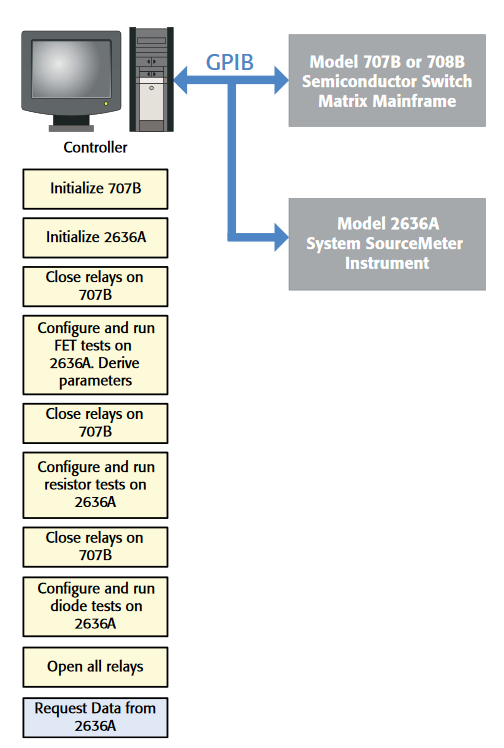
This configuration is represented in Figure 6. Time associated with tasks shaded in yellow is included in the throughput comparison. The time to perform tasks shaded in blue is not included in the throughput comparison. Using this method, the GPIB controller, typically a PC, maintains all test configurations and controls every measurement: Sends commands to the switch to open and close as necessary. Sends commands to the SourceMeter instrument to source and perform measurements.
Option 2: Optimized Switch - SourceMeter Configuration
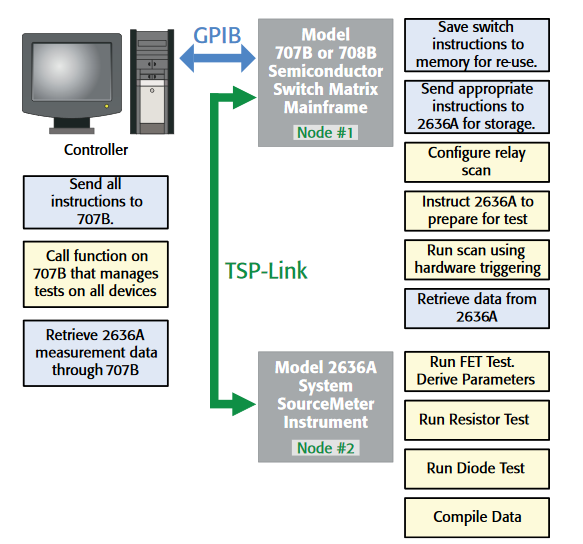
This configuration is illustrated in Figure 7. Time associated with tasks shaded in yellow is included in the throughput comparison. The time to perform tasks shaded in blue is not included in the throughput comparison.
Using this method, the controlling PC sends out all instructions required for 707B and 2636A as scripts that reside on the instruments. Scripts that configure the switch and manage the overall test reside on the 707B. The 707B copies scripts relevant for configuring the SMUs onto the Model 2636A. The switch then configures a scan list of relay crosspoints to be used during the test. After each path selection (one step in the scan list), the 707B sends a digital signal to the 2636A. After completion of all tests for one device, the 2636A sends a digital signal to the 707B. Once all tests are complete, the 707B requests data from the 2636A to return to the controller. Because frequent data transfers can degrade system throughput, the PC can retrieve this data when transfer time can be hidden in other lengthy system tasks, such as prober step.
Results
Option #2 results in approximately a 9% throughput improvement with the same quality of measurement results. This improvement is solely due to a reorganization of test software. No changes were made to the measurement methods, integration times, or test sequence. A second advantage that Option #2 offers is a closed-loop system. Triggering ensures that the switch is closed before a measurement (or test) is run on the SourceMeter instrument. In option #1, there was no verification of switch closure prior to the measurement on the SourceMeter instrument. As more tests, devices, and switch closures are added, the impact of a 9% improvement on overall test time becomes obvious.
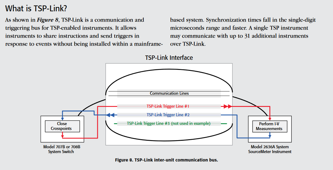
Using the Test Script Process (TSP®) embedded in each of the instruments and the TSP-Link® inter-unit communication bus to coordinate triggering and communication of instructions and data enhances overall test throughput. Fewer commands are sent by the controlling PC because multiple relay close/open commands are replaced by a scan. Also, saving test instructions on the 707B and 2636A eliminates the need to reload these commands each time the test is run. Command parsing time is also reduced because the controlling PC only sends the commands once over the communication interface. Lastly, hardware triggering coordinates instrumentation and eliminates time from unnecessary delays and polling in the PC software.
In a given parametric test operation, there could be several switch path selections and measurements for every prober step. With thousands of measurements to be made across a wafer, software and communication overhead times in unoptimized applications can have a major impact on the overall test time. The Models 707B and 708B, like the Series 2600A System SourceMeter instruments, feature TSP technology, a form of distributed computing that allows the instruments to assume some functions typically managed by the system controller and affords the fastest possible system timing.
TSP technology can be further exploited by executing tests in parallel. For instance, the Models 707B and 708B can be used to manage multiple source-measure instruments in order to characterize multiple test structures simultaneously. Adding another SourceMeter instrument to the previous example permits tests on the resistor and diode and transistor to be run simultaneously. Synchronizing the start of all tests on a test structure can be done easily by configuring all tests to start at a single digital signal on the TSP-Link interface. TSP builds trigger controller capabilities into the instrument, giving the user the ability to perform logical AND/OR operations on trigger signals from multiple instruments.
Optimizing Throughput with Non-TSP-Enabled Instruments
Although TSP instruments offer highly optimized throughput, this technology has not yet been incorporated in all Keithley instruments. What can be done to optimize throughput in configurations that include instruments without TSP?
Hardware triggering is an excellent way to speed up testing. The triggering capability available in the Models 707B and 708B can be used with any external instrument. For example, the 14-bit digital I/O port of the 707B and 708B can be used to interface with non-TSP-enabled instruments. Adapters are available to convert between the D-sub digital I/O connector and the Keithley Trigger-Link connector, which is standard on many of Keithley's SCPI-based instruments. For integrating instruments with BNC connections, the 707B/708B's digital I/O connector may be easily converted to BNC with readily available components.
Keithley's Automated Characterization Suite (ACS) software can be employed to optimize the operation of semiconductor parameter analyzers. ACS supports combining software written in a variety of languages (TSP/Lua, C, Python) in an application to control different pieces of instrumentation in a single, user-friendly interface. ACS provides the support needed to combine the TSP capabilities of the Models 707B and 708B and Series 2600A System SourceMeter instruments with the C-V measurement performance of the Model 4210-CVU, an option for the Model 4200-SCS Semiconductor Characterization System.
Keithley offers a number of custom-configured system options that combine ACS software, 707B/708B mainframes, Model 4200-SCS, and Series 2600A mainframes, including two versions of the S530 Automated Parametric Test System.

