Introduction
The Phase Locked Loop has become one of the most versatile building blocks in electronics. They are at the heart of circuits and systems ranging from clock recovery blocks in data communications to the local oscillators that power the ubiquitous cellular phones. The property of making its output frequency an exact multiple of the reference frequency makes the Phase Locked Loop (PLL) the circuit of choice for frequency synthesizers, for aligning the various clocks in synchronous systems and for a myriad of applications ranging from tracking satellite Doppler shift to sensing minute reactance changes in industrial proximity sensors.
Much work has been done to describe PLLs in terms of their function as linear feedback control systems. The linear steady-state approximation provides an accurate description of PLL operation for small variations about a stable locked state. Linear analysis is more than adequate to describe small signal effects such as the PLL response to small signal modulation, phase noise, or spurious. Linear analysis is mostly done in the frequency domain, with performance measurements made using traditional spectrum and network analyzers. PLLs, however, behave very differently from the linear models when far from lock, during switching transients, and when responding to large signal inputs. Non-linear operation often dominates critical parameters such as settling time, switching speed and capture range. Understanding both the linear and non-linear operation is also critical to meeting emissions requirements in frequency agile communications systems that use PLLs as part of frequency hopping oscillators. Non-linear analysis is most often done in the time-domain with performance measurements made using in-circuit probes and oscilloscopes.
The advent of large-scale mixed-signal integrated circuits have pushed much of the PLL circuitry onto monolithic ICs, making it impractical to probe the necessary signals. This creates a need for time domain measurements of frequency and phase using only the PLL output signal, which is generally available.
This paper presents an overview of phase locked loop operation including both linear and non-linear effects. It also shows measurements of these effects in both the time and frequency domains using Tektronix Real-Time Spectrum Analyzers.
Frequency and Time Domain

Tektronix Real-Time Spectrum Analyzers have the abilities to trigger on transient signals in either the time or frequency domain, to capture a seamless time-record of the signal, and to analyze the captured signal in the frequency, time, modulation, and code domains. This ability to operate across multiple domains make Tektronix real-time spectrum analyzers the ideal instruments to measure both the linear and the non-linear performance of phase locked loops.
PLL Basics
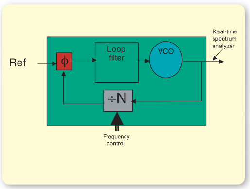
The phase locked loop is basically a control system that employs feedback to maintain the phase of the output signal in-step with the phase of a reference signal. More specifically, the PLL, when locked, controls the phase of the output signal to be N times the phase of the reference as shown on Figure 1. Similarly, the frequency of the output signal is then N times the reference frequency. Like all linear feedback control systems, PLLs have dynamic behavior characteristics that are commonly described using Fourier or Laplace techniques yielding transfer functions in either S or jω. The linear behavior described by the transfer function method is useful to analyze loop operation in the vicinity of lock. Non-linear effects dominate the behavior of the PLL in unlocked conditions such as when the frequency divider ratio is changed to switch frequencies over a large range.
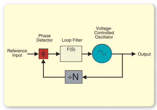
The building blocks common to most phase locked loops are the phase detector, the loop filter, the voltage controlled oscillator or VCO, and the frequency divider. Each of these building blocks has both linear and non-linear attributes to its operation.
Voltage Controlled Oscillator (VCO)
The Voltage Controlled Oscillator or VCO has an output frequency that is controlled through a tuning signal, as illustrated in Figure 2. This tuning signal is typically a voltage, as the name implies, but can be another variable. Current controlled oscillators, numerically controlled oscillators and even mechanically controlled oscillators are possible.
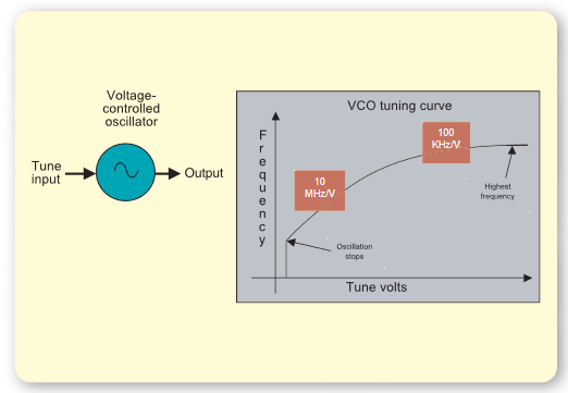
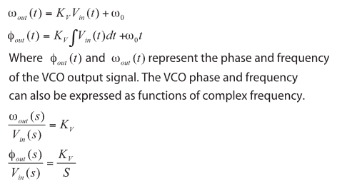
The tuning sensitivity of the VCO, KV, is its most significant parameter in linear analysis. VCOs are often non-linear, having tuning sensitivities that vary greatly over their tuning range. PLLs employing VCOs with large changes in the tuning sensitivity often require gain compensation to maintain consistent performance. VCOs also have other nonlinear behaviors that need consideration, including minimum and maximum tune frequencies, and tune voltages where oscillations stop or where undesired frequency components are generated.
VCO Linear Approximations
Frequency Divider
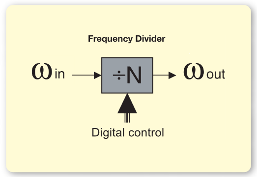
Phase locked loops used in frequency synthesis often use a frequency divider, as shown in Figure 3. This is most often a digital counter that produces one output pulse for N input pulses. Both the phase and frequency are scaled by the ratio, N. N is generally an integer. Fractional-N techniques exist to provide ratios that are not whole numbers.
Frequency Divider Linear Approximations
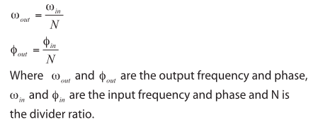
Integer-N dividers operate in linear fashion over their specified range of divisors and frequencies in that they scale the phase of the signal by a constant value. Fractional-N dividers achieve non-integer ratios by alternating among several integer values. This non-linear operation usually generates spurious signals that require filtering, correction or a combination of both.
Phase Detector
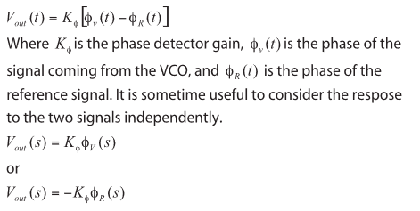
The Phase Detector, shown in Figure 4, is a circuit that produces an output signal that is proportional to the phase difference between two input signals.
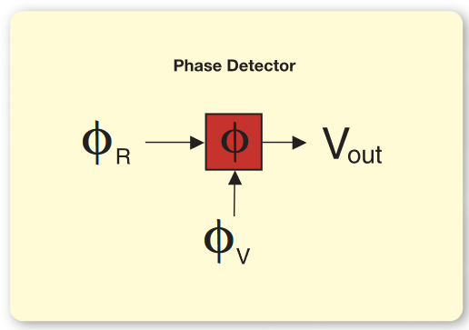
Phase Detector Linear Approximations
Phase Frequency Detector
The phase frequency detector is one of the most popular types of phase detectors. It is often used because it is implemented with inexpensive digital logic and because it inherently incorporates frequency steering when the PLL, in which it is embedded, is out-of-lock. Figure 5 illustrates the logic and timing of a basic phase frequency detector
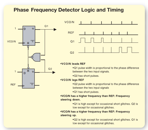
The phase frequency detector has a linear operating range of ±2π radians and often incorporates current or voltage sources that are gated on or off by the flip-flop logic states. The frequency steering operation pushes the loop in the direction of lock when the linear range is exceeded. Some phase frequency detectors also have a small “dead-zone” non-linearity in the vicinity of zero phase difference requiring a phase offset to force the quiescent lock point away from zero.
The phase frequency detector output resets whenever the phase difference between the two signals present at its inputs exceeds 2π radians. Successive resets, which can only be caused by an out-of-lock condition, place the phase frequency detector in frequency steering mode. In this mode, the phase frequency detector provides a pulsed signal that pushes the VCO in the correct direction for locking. The PLL is effectively open during frequency steering. The transients performance of PLLs during the frequency steering mode do not show the settling waveforms expected from a linear feedback control system. The phase frequency detector returns to phase detection mode once the output frequency is close to the frequency of lock.
Mixer Phase Detectors
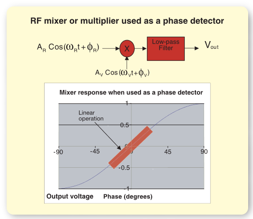
A multiplier or mixer can also be used as a phase detector. As Figure 6 illustrates, it can be shown that the output of the mixer is proportional to the sine of the phase difference between the two inputs.
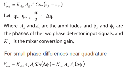
The linear approximation is valid for signals in the vicinity of quadrature. Non-linear operation dominates the behavior for large phase differences. It can be shown that the sinusoidal behavior of the mixer will drive the PLL into lock when the frequency error is small and the loop is within its capture range. PLLs using mixer-type phase detectors often use external pre-tuning or frequency steering mechanisms to bring the two frequencies within the capture range.
Loop Filter
The Loop Filter is used to tailor the PLL response in order to optimize its bandwidth, switching speed, settling time spurious levels or other design parameters. Loop filters often include integrators and are subject to the linearity concerns of the active devices that comprise the integrator circuits. Op-amps, for example, become non-linear as the output voltage clips when it nears the power supply voltages.
PLL Linear Operation
The operation of a PLL near lock is easily described using techniques developed for feedback control systems that yield a transfer function in S, the complex frequency parameter used in Laplace transforms.
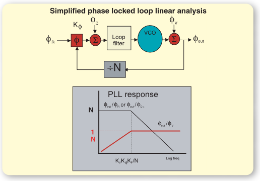
The transfer function to the various possible stimulus points can be found using conventional techniques. The responses to phase fluctuations in the reference, in the VCO and to signals injected at the phase detector output are explored here.
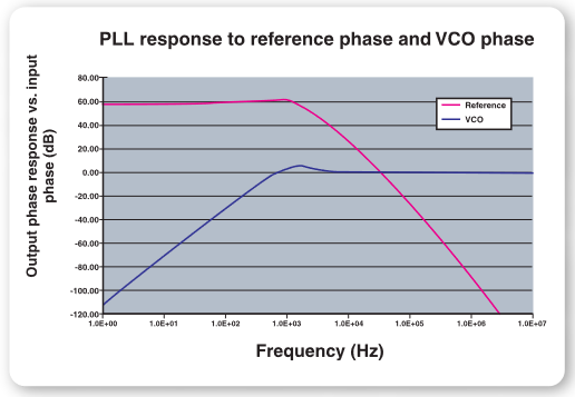
The PLL transfer function that describes its response to reference phase fluctuations has a low-pass shape. As shown in Figure 7, the output phase follows the reference phase fluctuations multiplied by N for frequency components below the PLL bandwidth. The output phase becomes independent of the reference for phase components above the PLL bandwidth. The response to signals added at the phase detector has a similar low-pass shape. The transfer function describing the PLL response to phase fluctuations in the VCO has a high pass shape. The PLL has no effect on the VCO phase for fluctuation components above the loop bandwidth but attenuates lower frequency components that lie inside the loop bandwidth. This property of PLLs is often used to improve the phase stability of an oscillator, where a reference signal with low phase noise is used to improve the phase noise of a higher frequency VCO. The phase noise of the reference and the phase detector noise multiplied by N dominate low frequencies while the phase noise of the VCO dominates high frequencies. Other sources of phase modulation (noise, spurious, etc.) are similarly affected by the PLL. Only VCO, reference and phase detector noise are considered here for simplicity.
Practical Loop Filter
A practical PLL filter contains an integrator, a pole and a zero to shape the PLL response and an additional pole to filter out reference frequency feed-through spurs. As shown in Figure 8, a PLL containing an integrator in the loop filter is known as a Type 2 phase locked loop.


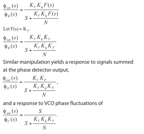
The PLL response then becomes a 4th order function. As shown in Figure 9, the responses of a PLL to phase fluctuations in the reference and to signals summed at the phase detector are low-pass functions given by
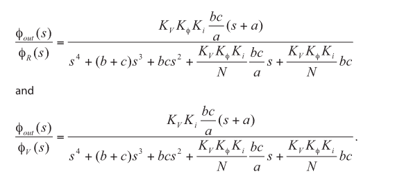
The response of the PLL to VCO phase fluctuations is a high-pass function given by

Linear Analysis Example: The Effect of a PLL Response Effect on Phase Noise Performance
Phase Noise in Oscillators
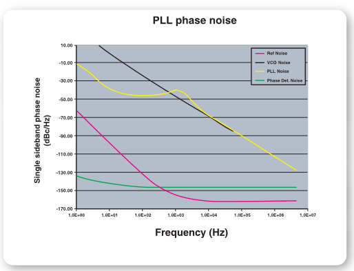
All oscillators exhibit phase fluctuations. These fluctuations can be interpreted as irregularities in the exact time of each zero crossing, called jitter. The fluctuations can also be viewed as random phase modulation and called phase noise. Phase noise is most often expressed as a ratio of sideband power in a one Hz bandwidth to the signal power expressed in dBc/Hz. Figure 10 shows the phase noise profile of a typical reference signal from a low-noise crystal oscillator, the noise from a 2.4 GHZ VCO and the noise contribution of a phase detector. Also shown is the composite noise at the PLL output. Note that the output noise is significantly lower than the unlocked VCO noise for low frequency offsets and only exceeds the VCO noise in a narrow region near the loop bandwidth. Further optimization of the loop filter and improvements to the noise performance of the phase detector can improve the system phase noise beyond the performance shown here.
Measuring Phase Noise
Tektronix Real-Time Spectrum Analyzers can measure phase noise directly using the Carrier to Noise Ratio measurement (C/N). This measurement can be made with direct readings that provide the C/N in a specified bandwidth as well as the C/N in a 1 Hz bandwidth (C/No). An alternate approach is to use marker readings which provide marker power readings in a given resolution bandwidth as well as the power normalized to a 1 Hz bandwidth.
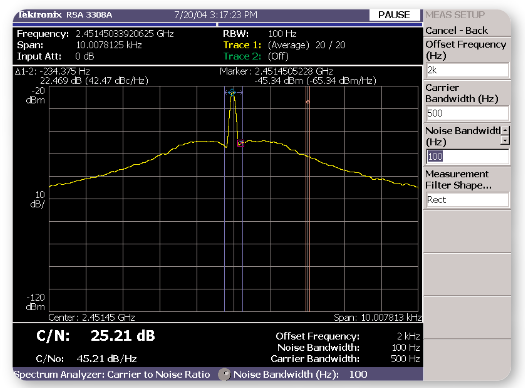
Figure 11 shows the C/N measurement screen. In this case, the C/N is measured at a 2 KHz offset from the carrier center frequency. The C/N in a specified noise bandwidth of 100 Hz is 25.21 dB and the C/No is 45.21 dB as shown on the lower left corner of the screen.
Measurements made at various offsets are shown in Table 1. The measurement bandwidth is varied depending on the span used and the amount of noise averaging desired.
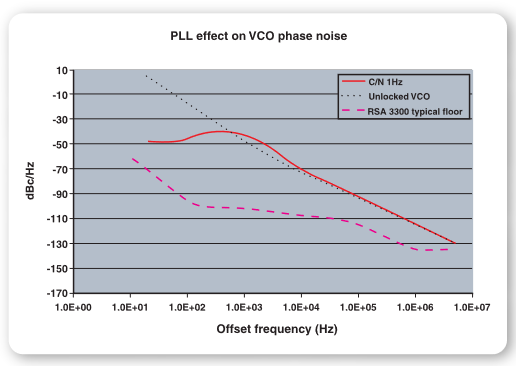
Figure 12 shows a plot of the PLL phase noise measured above superimposed on the phase noise of the unlocked VCO. The typical measurement floor of the Tektronix RSA Series Real-Time Spectrum Analyzer is also shown.
Measuring Spurious Signals
There are many sources of spurious signals that can affect the output of a phase locked loop. Clocks driving digital circuitry, power supply switching frequencies, local oscillators in nearby conversion stages, and inter-modulation products among the various frequencies present in a module are just a few. One source of spurious signals that is universally present in PLLs is the reference signal. The phase detector output often consists of pulses that occur at the reference frequency, generating frequency components at multiples of the reference frequency. Reference frequency rejection is often designed into the loop filter to reduce the level of reference-related spurious. Analytical methods to predict the level of reference spurs are imperfect at best. Measurement is often a necessary part of the design process and an essential part of verification.
Measurements of spurious signals are most often done in the frequency domain. Resolution Bandwidth (RBW) is selected to resolve the desired spurs from any noise that is present and trace averaging is used filter out any additional displayed noise. Marker delta provides a convenient way to identify the spurious signal frequency and its amplitude relative to the PLL output frequency
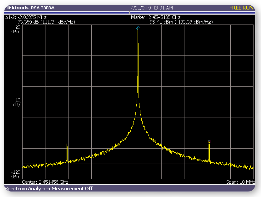
Figure 13 shows a marker delta measurement of the reference spurs in a PLL. The measurement shows spurious signals at a level 73.4 dB below the carrier and a frequency offset of 3.07 MHz, the PLL reference frequency.
Non-Linear Operation: Measuring Transient Behavior
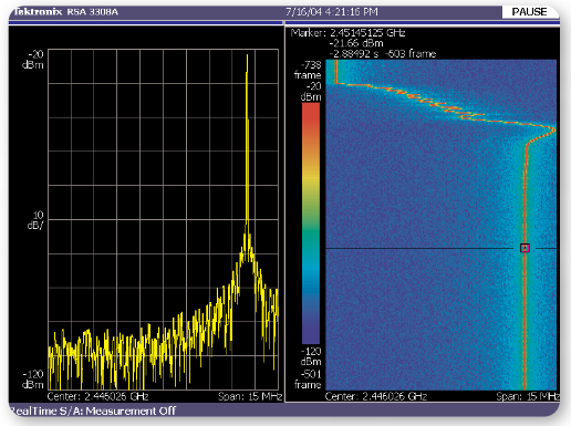
Figure 14 plots the frequency output of a PLL synthesizer as it switches from 2439.17 MHz to 2451.46 MHz. A significant part of the settling time is consumed by the non-linear frequency steering operation of the phase frequency detector. Linear operation begins after 550 microseconds where the phase detector is within range and the loop closes. Linear analysis can predict behavior beyond this point. Time-domain modeling, usually done using Z-transform techniques, and direct measurement are needed for the non-linear portion of the switching transient.
Traditional Measurement Method
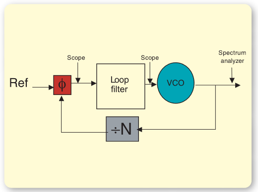
Phase locked loops have traditionally been implemented using discrete components where each of the building blocks discussed above is available for probing and measuring. Figure 15 shows how transient behavior in such a system can be measured by probing the VCO tune line, the phase detector output and the VCO output in order to observe transient behavior directly. This method of probing key points in the PLL signal path is very useful in cases where the required probing points are accessible.
PLLs Integrated Into Multi-Function Integrated Circuits
Cellular phones, wireless LAN cards, serial data communications systems, etc. are increasingly being implemented as one-chip subsystems. The entire PLL is often part of an integrated circuit that contains many other building blocks. Probing is not a practical option once the IC has been packaged, and few if any signals are available on IC pins. PLL characterization must be made using only the signals that are available. The natural signals are the output frequency, the reference frequency and any control inputs. Much, if not all, of the needed information can be obtained by observing the frequency trajectory of the PLL output on a Real-Time Spectrum Analyzer as shown in Figure 16. The RTSA can be triggered externally (using signals from the control bus for example) or internally using frequency mask trigger.
Frequency Mask Trigger
The Frequency Mask Trigger can be set up to trigger an acquisition at the instant the spectrum crosses a pre-determined mask. In the case shown above, the mask is set up to trigger the instant the oscillator frequency crosses the destination frequency (2.45146 GHz) as shown at the topright trace above in Figure 17. The instant of the trigger occurs is marked by the blue T in the upper-left trace.
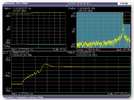
Viewing both pre-trigger and post-trigger data as indicated by the green bar on the upper-left trace, allows the analysis of the frequency trajectory leading to the frequency switch as well as the trajectory after it is shown on the lower trace. The spectrum at a given point in time, indicated by the red bar in the upper-left trace, can be shown on the upper-right trace. The delta markers show a switching speed of 2.259 mSec for settling to within 100 KHz of the final frequency. The first 1.3 mSec of the switching time were occupied by frequency steering, the remainder by closed-loop settling.
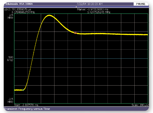
The difference between the linear and non-linear operation of the PLL can be illustrated by switching the frequency of the same PLL in a smaller step. Figure 18 shows the PLL frequency trajectory when switching from 2.44838 GHz to 2.45146 GHz, a 3.072 MHz step. The output frequency settling time to within 100 KHz of final frequency is now 781.8 µSec. The transient shape shows the expected step response of a closed loop system with mild overshoot and none of the non-linear steering behavior exhibited by the PLL when a larger step size was measured.
Time Dependent Spectrum Analysis
The spectral content of signals is often an important concern for the designers of communications systems.
Systems that switch frequencies during normal operation require care to meet spectrum mask requirements not only after full frequency settling but also during frequency transitions. The frequency content of a PLL output during switching may differ significantly from its frequency content after all transients are settled. The spectral content of transients can be a significant source of interference.
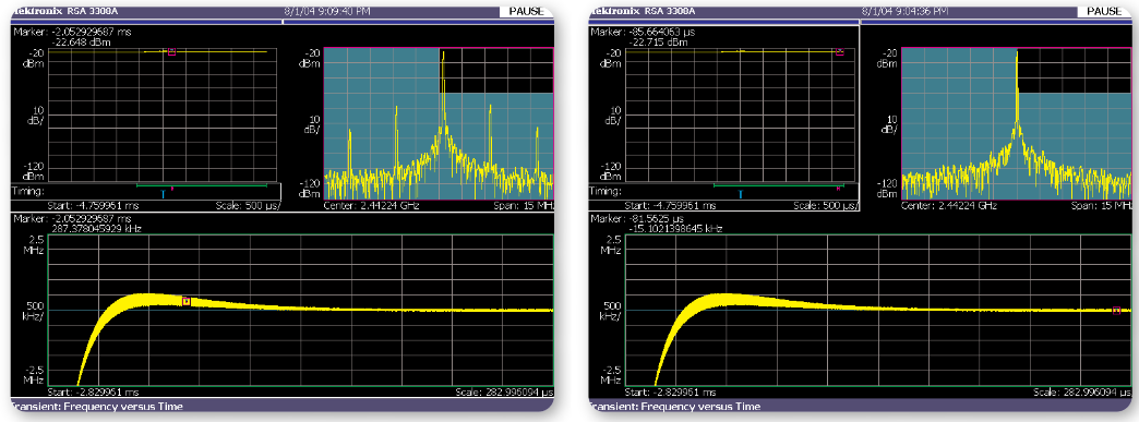
Figures 19 and 20 compare the spectrums of the PLL output during a switching transient with the spectrum after settling is complete. The upper trace shows the spectrum of a PLL output at a point in time where the transients are nearly settled as shown by the marker location. There is a large amount of reference related spurious at 3 and 6 MHz offsets from the carrier. The lower trace shows the spectrum after sufficient settling has taken place. Note that the reference related spurious signals are gone. There may also be significant differences in the occupied bandwidth and the noise level as well as in the center frequency
Conclusion
The PLL has become an indispensable building-block in a wide variety of communications systems. Increasing levels of integration have made simulation and analysis essential, requiring an understanding of both linear and non-linear behavior in the circuit elements that comprise the PLL. Integration has also placed the signal paths required for testing in inaccessible locations inside IC packages. RealTime Spectrum Analysis provides a valuable means to characterize, measure, and view the behavior of PLLs in the time, the frequency and the modulation domains, opening the door to previously hidden transient behavior

