お問い合わせ
ダウンロード
マニュアル、データシート、ソフトウェアなどのダウンロード:
フィードバック

Comprehensive Wafer Test Development and Testing Services
At Tektronix Component Solutions, we provide comprehensive wafer test development and testing services designed to meet the most demanding semiconductor applications. Our state-of-the-art facilities span over 45,000 sq. ft., featuring Class 10,000 (ISO 7) and Class 1000 (ISO 6) clean rooms that ensure optimal conditions for wafer processing.
We specialize in testing a wide range of wafer sizes, including 4", 6", 8", and 12" (100mm, 150mm, 200mm, 300mm). Our capabilities encompass analog, digital, and mixed-signal testing, with advanced test equipment supporting frequencies up to 110 GHz. We offer precise wafer test temperature ranges from -40°C to 200°C, ensuring accuracy and repeatability in diverse environments. Our services feature a wide range of probing technologies and support for both vertical and membrane-style probe cards, making us a trusted partner for all your wafer testing needs.

Our Wafer Test Workflow
Project Kick-off & Planning
We collaborate with customers to review requirements, define the testing framework, and select the best testing platforms, probing technologies, and test vectors to meet project objectives.
Development Cycle
Our team develops hardware and software in parallel to meet complex testing needs. Hardware efforts focus on custom probe test boards, collaboration with probe head vendors, and addressing application-specific challenges. On the software side, we create tailored test scripts, ensure full coverage, and integrate with the CSO custom database. Rigorous design review cycles ensure quality and alignment across disciplines.
System Integration & Debug
We integrate the test system with hardware such as probe cards, RF equipment, and ATE systems, followed by rigorous debugging to ensure smooth operation. Initial power-up confirms the functionality of the device, hardware, and software.
Characterization & Finalization
Refined hardware and software enable precise test methodologies for effective experimentation during characterization and limit-setting. Our team specializes in first turn-on of new devices, leveraging expert resources to troubleshoot, debug, and collaborate with design engineers to resolve challenges.
Validation & Readiness
We conduct statistical analyses, including GR&R studies, to ensure consistent, reliable results. Production readiness tasks are completed, reviewed internally, and presented to the customer for final approval.
Our Competitive Edge
Turn-Key Solutions for Wafer Value Stream
For projects requiring wafer processing (e.g., wafer bumping, thinning, dicing), we maintain relationships with various domestic and international industry suppliers and offer supply chain management capabilities to enable a turnkey solution for your microelectronic parts.
- Wafer Fabrication
- Wafer Bumping
- Secure Storage
- Wafer Probing
- Wafer Inspection
- Die Preparation Services
Best in Class Wafer Test Services
Beyond standard development and testing, we offer a wide range of automated wafer test processes that greatly improve accuracy and repeatability, including:
- Automated wafer handling
- Automated probe card changing
- Automated optical probe tip inspection
- Automated optical probe mark inspection
- Automated probe tip cleaning
Customized Wafer Probing
Tektronix employs a team of electrical and mechanical design engineers that can develop customized wafer probe cards and test solutions to meet the most demanding requirements.
For projects requiring wafer processing (e.g., wafer bumping, thinning, dicing), we maintain relationships with a variety of domestic and international industry suppliers and offer supply chain management capabilities to enable a turnkey solution for your microelectronic parts.
Tektronix employs a team of electrical and mechanical design engineers who can develop customized wafer probe cards and test solutions to meet the most demanding requirements.
Understanding Wafer Testing
Ensuring Quality in Semiconductor Manufacturing
Wafer Test (also referred to as Wafer Probe) is a vital step in the Semiconductor Value Stream, focusing on electrical screening and consumption of Known Good Die (KGD). It involves probing individual semiconductor devices on a wafer to identify defects and confirm functionality before further manufacturing.

What Does Wafer Testing Entail?
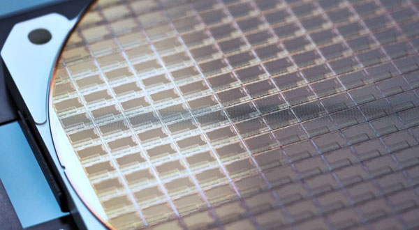
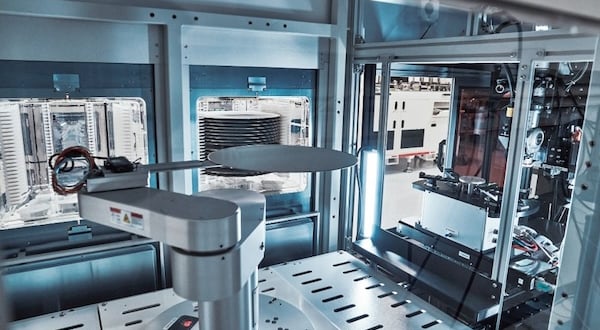
First, let’s start with understanding the form factor of a modern wafer. A wafer is essentially a disc that is no greater than 3/4 mm thick and up to 300 mm in diameter. To put this into perspective, imagine a silicon disc that is half the thickness of a dime and a foot in diameter. Due to the form factor and fragile nature of the wafer, it is impractical to process a wafer by hand (especially since most wafers are bumped). Therefore, in today’s semiconductor testing environment, fully automated equipment is utilized to enable the process. The automation includes both a wafer prober to handle the wafers, a programmed test solution to perform the electrical testing, and robotic equipment to perform inspection and sort wafers.
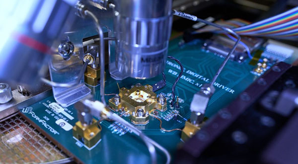
To connect to the Device Under Test (DUT), a probe head and card must be designed (typically unique to each Integrated Circuit - IC) and integrated with the test station and wafer prober to form the test solution.
A cassette of wafers (up to 25 at a time) is loaded onto the prober, and the screening process begins. An individual wafer is selected, placed on a stage, and manipulated so that each device on the wafer can be accessed and electrically tested. The data for each IC is collected, and a digital map is generated identifying the location and Pass/Fail status. Once complete, the wafer(s) can be sent to the dicing process so that the KGD are ready to be consumed at the next level.
What Are the Benefits of Wafer Testing?
In the era of System on a Chip (SOC) and Heterogeneous Solutions, where integrating multiple complex ICs per package is the norm, the significance of KGD entering the packaging stage cannot be overstated. Wafer Test plays a crucial role in defect detection, ensuring that non-conforming components are identified and prevented from reaching the next stage of production. Paired with continuous Process Monitoring, it empowers engineers to address issues at an early stage, significantly contributing to yield improvement and reduced production costs by eliminating defects in the early steps of the Semiconductor Value Stream.
ウエハ・プローブに関するよくある質問
一般的な試験周波数帯域は?
一般的な試験温度範囲は?
テスト・ソリューションは、室温(25°C~40°C)での-40°C、+100°C、+125°Cの一般的な温度に対応するよう構成されています。
具体的には、プローバのTEL P8XLモデルは-55°Cの低温まで到達可能で、Accretechモデルは-40°Cまで対応可能です。
今日のウエハ・テストが直面する課題とは?
ウエハ・テストは複雑なサービスのため、特に重要な課題のみをご紹介します。
まず第一に、1つのパッケージに複数のデバイスを統合するヘテロジニアス・ソリューションの普及により、テスト・プロセス全体を通じてこれらのコンポーネントの追跡と管理が複雑化しています。各要素の完全性を確保するため、堅牢な部品識別とトレーサビリティ・システムが必要となっています。

第二に、2.5Dソリューションへの移行により、集積回路(IC)の相互接続密度が大幅に増加しています。例えば、ICの相互接続間隔が0.150 mmから0.030 mmに縮小する可能性があります。これはXY軸ともに5倍の縮小となり、相互接続密度は最大25倍に増加します。このような厳しい間隔と平面度要件に対応するため、新しいプロービング・ソリューションと手法の開発と認定が必要となっています。
最後に、ICソリューションの需要拡大に伴い、ウエハ・テストへの要求も拡大しています。取り扱いによって引き起こされる欠陥の可能性を排除するため、手動での取り扱いをなくすことが最重要課題となっています。
課題の解決策は?
ウエハ・テストのトレーサビリティを向上させるため、(人間が読み取り可能な固有識別子をレーザー刻印する代わりに)IC設計に不揮発性メモリを直接統合することで、正確な追跡が容易になります。これにより、各ICのウエハ・ロット、ウエハ番号、行/列情報を容易に取得でき、製造プロセス全体を通じて部品の系統と追跡の改善に貢献します。不揮発性メモリを活用することで、半導体業界はトレーサビリティ・メカニズムを強化し、半導体バリュー・ストリームを超えてICのトレーサビリティを維持することができます。
半導体業界が2.5Dソリューションを取り入れていく中で、IC上の相互接続密度の増加は新たな課題をもたらします。この課題に対処するには、テスト・プロバイダ、ウエハ・テスト装置ベンダー、プローブ・ソリューション・サプライヤ間の連携強化が必要な革新的なプロービング・ソリューションが求められます。協力して取り組むことで、この移行に伴うより狭い間隔と高い平面度要件に適切に対応できる先進的なプロービング手法を実現できます。

ウエハ・テストにおける包括的な自動化への需要は、改善のための重要な方向性です。人の手による取り扱いステップを効率的に排除できるこれらのシステムは、不要な欠陥の削減とテスト環境全体の効率向上につながります。検査プロセスにAIと機械学習を組み合わせることで、スクリーニング時間と効果を改善し、人依存の手順に関連する課題に対処できます。
ウエハ・テストの未来は?
ウエハ・プローブの一般的な用途は?
ウエハ・プローブは、半導体業界でプロセス管理、デバイス特性評価、故障解析、信頼性試験など、さまざまな用途に使用されています。
ウエハ・プローブの種類は?
ウエハ・プローブには、手動プローブ、半自動プローブ、全自動プローブなど、いくつかの種類があります。手動プローブは作業者が手動でウエハを各テストサイトに移動させる必要がありますが、半自動および全自動プローブは自動的にウエハを各テストサイトに移動させることができます。
ウエハ・プローブを選ぶ際に考慮すべき点は?
ウエハ・プローブを選択する際は、プローブ・チップのサイズと形状、プローブ・チップの材質、プローブの平面度、プローブの位置決め精度などの要因を考慮することが重要です。その他の考慮すべき要因には、プローブの数、ウエハのサイズ、必要なスループットなどがあります。