Introduction
The continuing push for more devices on each chip and faster clock speeds is driving the demand for shrinking geometries, new materials, and novel technologies. All of these factors have a tremendous impact on the lifetime and reliability of individual devices due to greater fragility, higher power density, more complex devices, and new failure mechanisms. Processes that once produced devices with 100-year lifetimes may now yield only 10-year lifetimes, which is uncomfortably close to the expected operating life of systems using these devices. The smaller margin of error means that lifetime reliability must be designed in from the start and constantly monitored, from device development through process integration and into production; even small lifetime changes can be catastrophic to today’s devices.
Although reliability testing can be performed at the packaged device level, many IC makers are migrating to wafer level testing for several reasons, including the need to test further upstream in the manufacturing process. Wafer level reliability (WLR) testing also eliminates much of the time, production capacity, money, and material lost if the packaged device fails. The turnaround time is significantly less because a wafer can be pulled directly off the line and tested without waiting for device packaging, which can be up to a two-week process. Much of the testing is the same in both packaged device and WLR testing, allowing for relatively easy migration to wafer level testing.
Stress-Measure Technique for WLR Tests
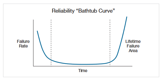
Stress-measure testing is a technique commonly used to evaluate operating lifetimes and wear-out failure mechanisms in semiconductor devices. This testing is focused on failures on the right-hand side of the typical failure rate bathtub curve (Figure 1), that is, failures that aren’t associated with infant mortality or manufacturing failures.
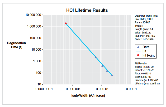
Stress-measure tests can quickly generate curves that are extrapolated to predict the operating lifetime of devices. Such data are used to evaluate device designs and monitor manufacturing processes. Because typical device lifetimes are measured in years, techniques are needed to accelerate the testing. The most efficient method is to over-stress the device, measure degradation trends of key operating parameters, and extrapolate the data to the full lifetime. In Figure 2, for example, the lower right portion of the curve (collected data) was generated using high stress conditions. The data generates a line that can be used to predict device lifetime under normal operating conditions (upper left portion of the curve).
Common WLR tests that use stress–measure techniques include Hot Carrier Injection (HCI) [1] or Channel Hot Carrier (CHC), Negative Bias Temperature Instability (NBTI) [2], Electromigration [3], Time Dependent Dielectric Breakdown (TDDB) [4] and Charge to Breakdown (QBD) [5] tests. These tests have become critical in mainstream CMOS device development and process control.
WLR Test Instrumentation Trends and Requirements
New scale factors and materials now require modifications to these established tests and demand instrumentation features that can implement the new techniques.
Reliability tests have evolved to match the needs of new device designs and materials. Although HCI is still an important reliability concern, engineers must now be concerned about NBTI for PMOS [6], charge trapping for high κ gate transistors [7], and cross effect between NBTI, TDDB and HCI, such as NBTI enhanced hot carrier [8], and TDDB enhanced NBTI [6]. To deal with these new phenomena, measurement methodology has evolved from DC stress and measurement to a point where both DC and pulse stress are now used to study degradation relaxation effect. Furthermore, instrumentation now includes more comprehensive device characterization suites, which include DC I-V, C-V, charge pumping, and charge trapping. Table 1 summarizes some WLR test trends.
| Traditional | New | |
| Main Device Degradation Mechanism | HCI Charge Trapping |
HCI Charge Trapping NBTI/PBTI NBTI–HCI TDDB–NBTI |
| Methodology | DC Stress | Pulse/DC Stress |
| DC Measure | Comprehensive Characterization (I-V, C-V, CP) |
Table 1. Recent Wafer Level Reliability test trends.
These evolving test requirements are challenging engineers to find the right instrumentation for efficient device and process development. The tool selected should be sensitive enough to capture all the pertinent details of parameter degradation due to stress and flexible enough to adapt to nontraditional WLR tests, such as stress C-V, NBTI, etc. This tool should also be extendable so that it’s unnecessary to buy a completely new system every time a new test issue comes up. Finally, the tool should be easy to understand so that users can focus valuable time on interpreting data, not on learning to use the test system.
In terms of features, a modern reliability test stand must provide the following:
- Hardware and software that accelerates testing without compromising accuracy and extrapolated lifetimes.
- Control of a semi-auto or auto-prober with a thermal chuck.
- Drivers to control instruments, probers, chucks; create tests; execute tests; and manage data.
- Flexibility to accommodate user-changeable tests and stress sequences for new materials and failure mechanisms.
- Analysis software that provides easy extraction of test parameters and a plotting tool.
Capabilities of 4200A-SCS and 4225-PMU Ultra-Fast I-V Module
The 4200A-SCS is a modular, fully integrated parameter analyzer with wafer level reliability test enhancements. This system allows I-V, pulsed I-V, and C-V characterization of semiconductor devices and test structures. Its advanced digital sweep parameter analyzer combines speed and accuracy for deep sub-micron characterization. The 4200A-SCS can provide up to nine slots for source-measure unit (SMU), capacitance-voltage unit (CVU) or pulse-measure unit (PMU) instrument cards, and control other external instruments, such as a switch matrix, LCR meter, and probe station. This can be done via GPIB, Ethernet, or RS-232 connections. The software includes a test plan manager, interactive test setup interface, Excel-like data sheet, graphing capability. It offers the flexibility to be used in an interactive manual mode (for single test operation during development) or in more automated production use cases.
The 4225-PMU Ultra-Fast I-V Module is a single-slot instrument card for the 4200A-SCS. It has two channels of voltage pulse sourcing with integrated, simultaneous,real-time current and voltage measure for each channel. This module is the hardware core of the ultra-fast I-V measurement capability essential for characterizing NBTI and PBTI degradation in microseconds, allowing for more accurate lifetime measurements for Designed-In Reliability (DIR) that support modeling for device and circuit design. It integrates a two-channel waveform generator with high speed voltage and current measurement capabilities, a deep measurement buffer, and a real-time test execution engine.
The 4225-RPM Remote Amplifier/Switch is an optional addition to the 4225-PMU. Its small enclosure is designed to be located near the device under test (DUT); it provides the lower-current measurement ranges necessary for characterization of many time-resolved reliability tests. By making it possible to locate the pulse source close to the DUT, the 4225-RPM helps minimize the cable length and corresponding cable parasitic effects to provide improved pulse shape and higher speed measurements. In addition, the 4225-RPM provides switching for the 4200A-SCS’s source measurement units (SMUs) and multi-frequency capacitancevoltage unit (CVU) signals to allow for high resolution DC measurements and C-V measurements without re-cabling.
Pulse source and measure tests can be performed using the 4225-PMU; tests requiring pulse sourcing but no corresponding pulse measurement can be performed with the 4220-PGU pulse-only card. One typical configuration with pulse source-measure capability would be a 4200A-SCS system that consists of four SMUs, two 4225-PMUs and four 4225-RPMs. This system would then have four SMUs and four pulse I-V channels (pulse source and measure), with the RPMs allowing for switching between pulse and SMU test resources. This four-channel system provides either DC or pulse source and measuring for a four-terminal test device or for measuring two terminals (for example, gate and drain) on two test devices.
For Ultra-Fast BTI (Bias Temperature Instability) testing for leading-edge silicon devices, a separate package (4200-BTI-A) [9] is available, consisting of one 4225-PMU, two 4225-RPMs, and Automated Characterization Suite (ACS) software. In addition to a wafer mapping capability, the ACS package includes routines to simplify the creation of on-thefly techniques and other popular techniques for minimizing the off-stress time to reduce the recovery effect inherent in silicon devices exhibiting the BTI behavior. See the sidebar titled “Ultra-Fast BTI Package” for more information.
Using the Clarius+ Software for WLR Testing
The Clarius+ software tool set supplied with the 4200A-SCS system includes a set of example projects for WLR testing. The projects include a stress–measure loop with configurable test- and project-level exit logic and a site loop for stepping through sites on a wafer [10]. Figure 3 shows the HCI sample project. The graph shows a particular parameter being tracked over time, with each dot representing a different measure cycle after a stress cycle. The left-hand window is the sequencer, which shows the order of measurement tests and the overall structure of the project. Several projects for WLR testing are in the Clarius Project Library, including:
- Hot Carrier Injection (HCI)
- Negative Temperature Bias Instability (NBTI)
- Electromigration (EM)
- Charge to Breakdown (QBD)
Hot Carrier Injection (HCI) Degradation
HCI degradation is a fairly important reliability concern in modern ULSI circuits. Charge carriers gain kinetic energy as they are accelerated by the large electric field across the channel of a MOSFET. Although most carriers reach the drain, hot carriers (those with very high kinetic energy) can generate electron-hole pairs near the drain due to impact ionization from atomic-level collisions. Others can be injected into the gate channel interface, breaking Si-H bonds and increasing interface trap density. The effect of HCI is time dependent degradation of device parameters, such as threshold voltage (VT), drain current in the linear and saturation region (IDLIN, and IDSAT), and transconductance (gm).
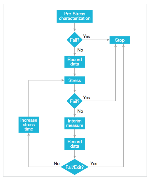
A typical HCI test procedure consists of a pre-stress characterization of the DUT, followed by a stress and measurement loop [11] (Figure 4). In this loop, devices are stressed at voltages higher than normal operating voltages. Device parameters are monitored between stresses and the degradation of those parameters is plotted as a function of accumulated stress time (Figure 2). Prior to conducting this stress and measurement loop, the same device parameters are measured to serve as baseline values.

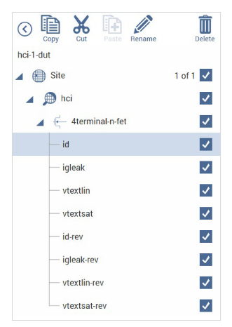
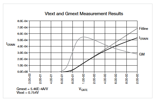
Hot carrier parameters monitored include VT, gm, IDLIN, IDSAT, and IDLEAK. These parameters are initially measured before stress and re-measured at each cumulative stress time. The IDLIN is the measured drain current with the device biased in the linear region; IDSAT is the measured drain current with the device biased in the saturation region. VT and gm can be determined using either constant current or extrapolation methods. In the extrapolation method, the VT is determined from the maximum slope of the IDS vs. VGS curve. Figure 5 shows a screen capture of the hci-1-dut project tests in Clarius. The 4200A-SCS’s Formulator Tool greatly simplifies extracting these parameters. Built-in functions include Differentiate to obtain gm, a MAX function to obtain the maximum gm (Gmext), and a least squares linefit function to extract VT (Vtext). The formulas to calculate these parameters can be found in the HCI projects supplied with the 4200A-SCS, and corresponding tests in test libraries. Figure 6 illustrates the Formulator’s automated data analysis capability.
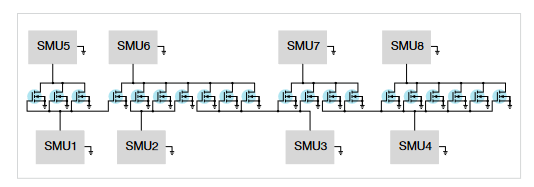
It is easy to perform an HCI test on a single transistor. However, each HCI test typically takes a long time to complete, so it is desirable to have many DUTs stressed in parallel, then characterized sequentially between stresses to save time. A switch matrix is needed to handle the parallel stresses and sequential measurements between stresses. The 4200A-SCS provides the stress voltages and measurement capability, while the switch matrix enables parallel stress and sequential measurements of multiple devices. Figure 7 illustrates a connection diagram using eight SMUs (for total of eight different drain and gate stress biases) plus a ground unit (for ground terminal) to stress 20 transistors in parallel. Table 2 lists the HCI test templates available in the test library.
| Project | Description |
| hci-1-dut | HCI project on one four-terminal n-MOSFET. Parameters monitored between two successive stresses include IDLIN, IDSAT, Ig, VT, and gm. Those parameters are measured on both forward (normal operation condition) and reverse (reverse source and drain bias) conditions. The subsite plan is configured for subsite cycling using DC voltage stressing |
| hci-4-dut | HCI project on two four-terminal n-MOSFETs and two four-terminal p-MOSFETs with a switch matrix. Parameters monitored between two successive stresses include IDLIN, IDSAT, Ig, VT, and gm. Those parameters are measured on both forward (normal operation condition) and reverse (reverse source and drain bias) conditions. The subsite plan is configured for subsite cycling using voltage stressing. Also, if fewer than four devices are tested, it is possible to deselect the unwanted device plan in the project tree or modify it for more devices. |
| hci-pulse | HCI project similar to hci-1-dut using AC stress. |
Table 2. HCI test library in Clarius.
Negative Temperature Bias Instability (NBTI)
NBTI is a failure mode that is problematic in PMOS transistors and getting worse as threshold voltage continues to drop and new materials are introduced into the gate stack to maintain device-level performance. NBTI degradation is measured by time dependent shifts in threshold voltages and is associated with slower operation, more leakage, and lower drive current under negative bias stress at high temperature.
The NBTI test is typically a stress–measure sequence loop. During the stress, negative gate bias voltage is applied with the rest of transistor terminals grounded. Between two consecutive stresses, drain current is measured at normal operating condition [12]. Degradation of drain current or threshold voltage is plotted as a function of stress time. All the stress voltages and subsequent measurements are done at high temperature (for example, 135 °C). The process flow for NBTI is similar to HCI, as shown in Figure 4.
Because of the recovery effect in BTI, the stress-measure feature available that uses the 4200A-SCS’s SMUs may not provide enough insight into the device degradation. As mentioned previously, a separate package (4200-BTI-A) is available for the 4200A-SCS that provides ultra-fast sourcing and measuring to characterize the degradation and recovery effects of BTI on modern semiconductor devices.
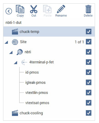
The project plan shown in Figure 8 includes actions to control the temperature of the chuck. The subsite plan will not start until the chuck reaches the specified temperature. After the first pre-stress cycle to perform characterization tests, subsequent cycles voltage stress the device for a specified period of time before again performing the tests. After the subsite plan is completed, the final step cools the chuck. In a parallel connection scheme, up to 20 devices can be stressed by voltage. Figure 7 shows an example of 20 parallelconnected devices being stressed by eight gate and drain voltages. See Table 3 for the NBTI test template available in the Clarius Project Library.
| Project | Description |
| nbti-1-dut | NBTI project on one four-terminal p-MOSFET. Parameters monitored between two successive stresses include IDLIN, IDSAT, Ig, VT, and gm. The subsite plan is configured for subsite cycling using voltage stressing. It also provides hot chuck control. |
Table 3. NBTI test library in Clarius.
Ultra-Fast BTI Package
Bias temperature instability testing may require sensitive, high speed measurements for accurate characterization. Assuming all other factors are constant, measurement physics largely defines the relationship between measurement speed and sensitivity. When making sub-millisecond measurements, all sources of noise must be taken into account; for sub-microsecond applications, quantum effects can’t be ignored. The 4200-BTI-A package provides the optimal combination of measurement speed and sensitivity for ultra-fast BTI testing. The 4225-PMU included in the package provides the ability to begin measuring BTI degradation as soon as 30ns after stress is removed and to measure transistor VT in less than 1 μs using ID–VG sweep method. Two 4225- RPM Remote Amplifier/Switch Modules add the function to switch automatically between low-level precision DC I-V (via standard SMUs) and ultra-fast I-V measurements with no need for re-cabling and improves single-pulse source and measurement performance by minimizing cable parasitic effects and increasing low current sensitivity. The package also includes the Ultra-Fast BTI software test module and the Automated Characterization Suite (ACS) software, making it easy to define stress timing, stress conditions, and a wide range measurement sequences from spot ID, On-The-Fly (OTF), or ID-VG sweeps. The test module allows measuring recovery effects as well as degradation. It also offers pre-stress and post-stress measurement options that incorporate the 4200A-SCS’s DC SMU instruments for high precision low-level measurements.
Electromigration
Electromigration is the phenomenon of material movement resulting from electrical current, and is a major reliability concern for metallization.
The isothermal electromigration test is an accelerated electromigration test performed on microelectronic metallizations. In the isothermal test, an attempt is made to maintain a constant mean temperature of the line under test. This is done by varying the stress current and therefore, the amount of Joule heating imparted to the line (based on the JESD61A-01 standard [13]).
The em-const-i project plan template is shown in Figure 9. The subsite plan (em) is configured for subsite cycling using current stressing on the single device (metal-line).
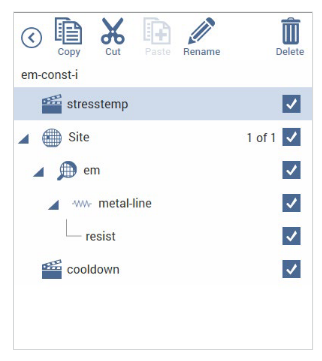
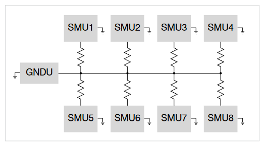
This project plan includes actions to control the temperature of the chuck. The subsite plan will not start until the chuck reaches the specified temperature. After the first pre-stress cycle to perform a characterization test on the device, subsequent cycles current stress the device for a specified period of time before again performing the test. After the subsite plan is completed, the final step cools the chuck. The em-const-i project plan can be modified to test additional devices. Each SMU in the test system can current-stress one device. Therefore, if there are eight SMUs in the test system, up to eight SMUs can be stressed, as shown in Figure 10. See Table 4 for the Electromigration test template available in the Electromigration test library.
| Project | Description |
| em-const-i | Electromigration project on one metal line (resistor) using constant current. At chuck temperature, a current is forced and the resultant voltage is measured; resistance is calculated. The subsite plan is configured for subsite cycling using voltage stressing. It also provides hot chuck control. |
Table 4. Description of Electromigration Project in Clarius.
Charge to Breakdown (QBD)
The QBD project plan includes the ramp-v test and the ramp-j test. These tests adhere to the JESD35-A standard procedures for wafer level testing of thin dielectrics [14]. This project (Figure 11) does not use subsite cycling.
- ramp-v: Voltage ramp test. This test uses a ramped voltage stress on capacitors, or gate oxide, to characterize the defects of dielectric at lower electrical fields.
- ramp-j: Current density ramp test. This test uses a ramped current stress on capacitors, or gate oxides, to characterize the defects of dielectric at higher electrical fields. The “test” is also able to achieve the bounded “J-Ramp” test, provided that the current is set to ramp up to a specified level and then held until breakdown. The bounded “J-Ramp” test provides a very repeatable charge-to-breakdown (QBD) measurement. See Table 5 for the Charge to Breakdown project description.

| Project | Description |
| qbd | qbd project on gate dielectric layer (capacitor). It consists of two qbd tests: ramp-v and ramp-j. An additional test performs an I-V measurement under normal work conditions to obtain input parameters for the ramp-v and ramp-j tests. |
Table 5. Charge to Breakdown test library in the Project Library.
Conclusion
Evolving design scales and new materials are making wafer level reliability testing more critical than ever. This is also driving the demand for reliability testing and modeling much further upstream, especially into the R&D process. Instrument manufacturers are responding with new reliability test tools that are faster, more sensitive, and highly flexible to help drive down the cost of semiconductor testing and shorten the time to market. Keithley’s 4200A-SCS parameter analyzer and package options provide the hardware and software necessary for fast and complete device characterization and reliability testing.
Find more valuable resources at TEK.COM
Copyright © Tektronix. All rights reserved. Tektronix products are covered by U.S. and foreign patents, issued and pending. Information in this publication supersedes that in all previously published material. Specification and price change privileges reserved. TEKTRONIX and TEK are registered trademarks of Tektronix, Inc. All other trade names referenced are the service marks, trademarks or registered trademarks of their respective companies.
012819 1KW-61526-0

