This Application Note
- Describes test fixtures and test modes for jitter tests
- Explains types of jitter tests
- Details the procedure for jitter testing with an exposed clock
10BASE-T, 100BASE-Tx and 1000BASE-T Ethernet are in widespread use, with new applications every day. 1000BASE-T Ethernet continues to thrive thanks to its reliability and interoperability. The latest commercial switches, routers, cable modems and network interface cards (NIC) commonly support 1G speeds. Cameras, medical devices and other embedded systems have adopted speeds up to 1G as well.
Achieving interoperability requires that each device meets IEEE 802.3 specifications, which include a common test methodology. Jitter tests are among these critical tests. Jitter is defined as any deviation of the actual signal transition time from the ideal transition time. Since Ethernet signals include embedded clock information, devices must limit jitter in order to achieve reliable data transfers.
The Test Fixture
All the devices must meet the specification as per the IEEE 802.3 standard and use a standardized test fixture. The test fixture must meet the functional requirements specified in section 40.6.1.1.3 of the IEEE 802.3 -2012 specification. The Tektronix fixture is model TF-GBE-BTP and it provides access to 10BASE-T, 100 BASE-Tx and 1000BASE-T signals from the RJ45 connector. In the case of 1000BASE-T signals, the four pairs of full duplex signals are separated into 4 different pairs accessible simultaneously on an oscilloscope. Each of the four pairs carries 250 Mbps of data with a clock rate of 125 MHz and employs five level signaling (PAM5) for transmission of data.
The test fixture is divided into 8 sections, TC1 to TC7. A companion PCB is used for calibration of return loss for short, load and ground. Each section of the main test fixture is used for testing different aspects of the signal. Two sections are important for jitter measurements:
- TC2: Templates Tests, Peak Voltage, Distortion and Droop measurements (without disturber) and Jitter
- TC3: Jitter

Transmitters must support four test modes, each of which outputs a different signal on the medium dependent interface (MDI). Jitter measurements on the 1G standard are accomplished using Test Mode 2 and Test Mode 3 signals.
The following chart provides a cross-matrix of tests and testcircuits on the fixture.
Table 1: Test to Fixture Matrix
| 1000 | COMPLIANCE TEST | TC1 | TC2 | TC3 | TC4 | TC5 | TC6 | TC7 | RLCF1 | JTC2 |
| Templates, Voltage, Droop, Distortion | ⬤ | ⬤ | ||||||||
| Jitter Master/Slave Unfiltered | ⬤ | ⬤ | ⬤ | |||||||
| Jitter Master/Slave Filtered | ⬤ | ⬤ | ⬤ | |||||||
| Return Loss | ⬤ | ⬤ | ||||||||
| Common Mode Output Voltage | ⬤ |
Table 2: 1000BASE-T Test Names/Test Patterns with relevant Test Fixture section
| TEST NAMES | TEST PATTERN | TEST FIXTURE |
| Template/Voltage | Test Mode 1 (TM1) | TC2/TC5 |
| Droop | Test Mode 1 (TM1) | TC2 |
| Distortion | Test Mode 4 (TM4) | TC2 |
| Return Loss | Test Mode 4 (TM4) | TC1 |
| Jitter | Test Mode 2 (TM2) / Test Mode 3(TM3) | TC2/TC3 |
| CM voltage | Test Mode 4 (TM4) | TC4 |
Jitter Tests
There are two separate cases for jitter measurements. The first is when an exposed clock (TX_TCLK) is available from the DUT and the other is when there is no exposed clock available. The specification defines limits when an exposed clock is available. However, there are no formal limits specified for the case in which no exposed clock is available. Measurements when no exposed clock is available are complicated and are meant only as informative tests. This application note covers the normative case in which an exposed clock is available.
There are two modes in which jitter must be measured: master mode and slave mode. In master mode the DUT operates as if the transmit clock TX_TCLK is sourced locally (by the DUT). In slave mode, the DUT operates as if the TX_CLK is coming from a link partner. Tests are further divided into filtered and unfiltered tests. The specification allows the use of either a physical filter or a digital filter in filtered mode. A physical filter may be used insofar as it does not significantly affect the impedance seen by the transmitter. Otherwise, a digital filter may be used to post-process the signal.

Jitter Testing with an Exposed Clock
Let us look at the case in which an exposed clock is available. The University of New Hampshire Interoperability Laboratory (UNHIOL) has defined the measurement procedures in the document Physical Media Attachment (PMA) Test Suite Version 2.5.
In exposed clock tests, the peak-topeak output of the differential signal from the MDI output is measured against the corresponding edge of TX_TCLK, which is labeled as JTXOUT. This measurement is made with the DUT operating in Test Mode 2 for the master and Test Mode 3 for the slave, and for all 4 pairs of signals (A, B, C, D). The peak-to-peak TX_TCLK jitter is measured for both conditions: unfiltered and filtered.
MASTER MODE
In master mode, the measurement is essentially the peak-peak jitter on the master TX_TCLK with respect to an “unjittered reference”. The IEEE specification does not describe the unjittered reference signal. However, the UNH-IOL PMA Test Suite Version 2.5 defines an unjittered reference as the straight line best fit (linear) of zero crossing of any specific capture of the signal under test. The master mode DUT is expected to be operating in normal mode, i.e. the device is connected to its link partner with a short UTP RJ45 cable.

The test mode 2 signal is a set of symbols controlled by the transmitter in master mode. On the Tektronix Test fixture, TC2 and TC3 are used for these measurements, as shown in the table above.
The unfiltered measurement calls for a minimum of 100 ms and a maximum of 1000 ms of capture. At minimum, a scope with 500 Mpts would be required when the signal is sampled at 5 Gs/s. Many oscilloscopes do not support this kind of memory, so implementation is permitted with multiple single shot captures to meet the required number of edges. In filtered mode, a maximum of 105 edges are required.
The integrity of the clocking system is validated in master mode jitter measurements. In master mode operation, under normal conditions, the peak-to-peak jitter value of the TX_TCLK when measured against an unjittered reference must be less than 1.4 ns.
For filtered measurements, the jittered TX_CLK is passed through a 5 kHz highpass filter with the transfer function:
The resulting peak-to-peak jitter value is added to the worst JTXOUT of the 4 pairs. This sum must be less than 0.3 ns.

SLAVE MODE
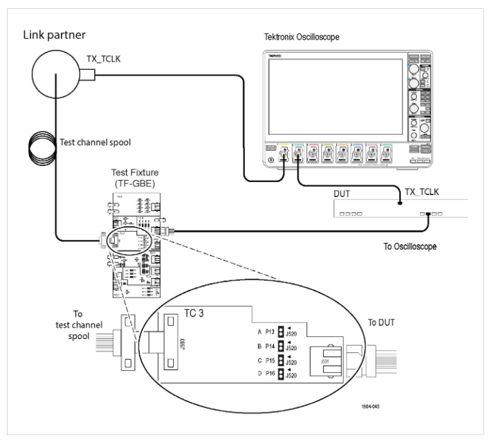
The test mode 3 signal is a set of symbols controlled by the transmitter in slave mode. On the Tektronix Test fixture, TC2 and TC3 are used for these measurements, as shown in the table above.
The unjittered reference for slave mode is defined as the master DUT TX_TCLK signal. The peak-to-peak jitter of both the DUT and the link master's clocks must be measured on the oscilloscope. Again, the master and the slave DUTs should be connected by the jitter channel described in the IEEE specification.

In this case, the link partner is the master and the DUT is the slave. The DUT and the link partner are connected by the prescribed jitter channel. The peak-to-peak jitter on the link partner TX_TCLK is determined by comparing with the unjittered reference and should have a capture duration of 100 ms to 1000 ms. The jittered TX_TCLK is passed through a 5 kHz high pass filter. The DUT peak-to-peak jittered TX_TCLK is then measured using the link partner’s TX_TCLK as a reference. This jittered signal is passed through a high pass filter of 32 kHz. The worst case JTXOUT is added to the DUT’s filtered output and the peak-peak jitter value of the master is subtracted. This value should be less than 0.4 ns. The high pass filter transfer function is defined by

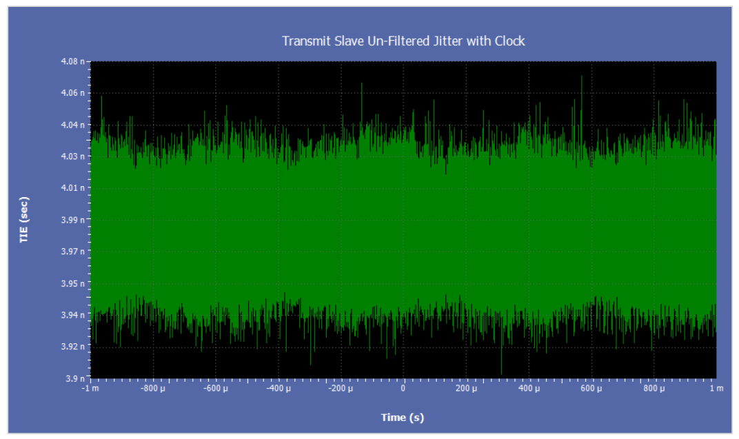
Table 3. Excerpt from a test report showing test results for a slave mode, unfiltered jitter test with exposed clock. The peak-topeak TIE is 0.17 ns.
| SLAVE UNFILTERED WITH TX_TCLK | |||||||||
| Pair | Measurement Details | Iteration | Measured Value | Test Result | Margin | Low Limit | High Limit | Units | Comments |
| BI-DA | SlaveUnfiltered_Jitter_With_TX_TCLK_ML_BI-DA | 1 | 0.1698 | Pass | H:1.2302 | N.A | 1.4 | ns | TIE Count :249998 |

Conclusion
Gigabit Ethernet continues to be used in new designs, thanks to widespread availability of devices, good performance and reliability. Jitter testing can be complicated, but it is necessary to validate the integrity of the clocking systems in this widely used technology.
References
- TekExpress® Ethernet Electrical Testing Application Printable Application Help
- IEEE 802.3 Standard for Ethernet Section Three Clause 40-2012
- UNH-IOL: GIGABIT ETHERNET CONSORTIUM Clause 40 Physical Medium Attachment (PMA) Test Suite Version 2.5
Find more valuable resources at TEK.COM
Copyright © Tektronix. All rights reserved. Tektronix products are covered by U.S. and foreign patents, issued and pending. Information in this publication supersedes that in all previously published material. Specification and price change privileges reserved. TEKTRONIX and TEK are registered trademarks of Tektronix, Inc. All other trade names referenced are the service marks, trademarks or registered trademarks of their respective companies.
07/20 48W-61719-0

