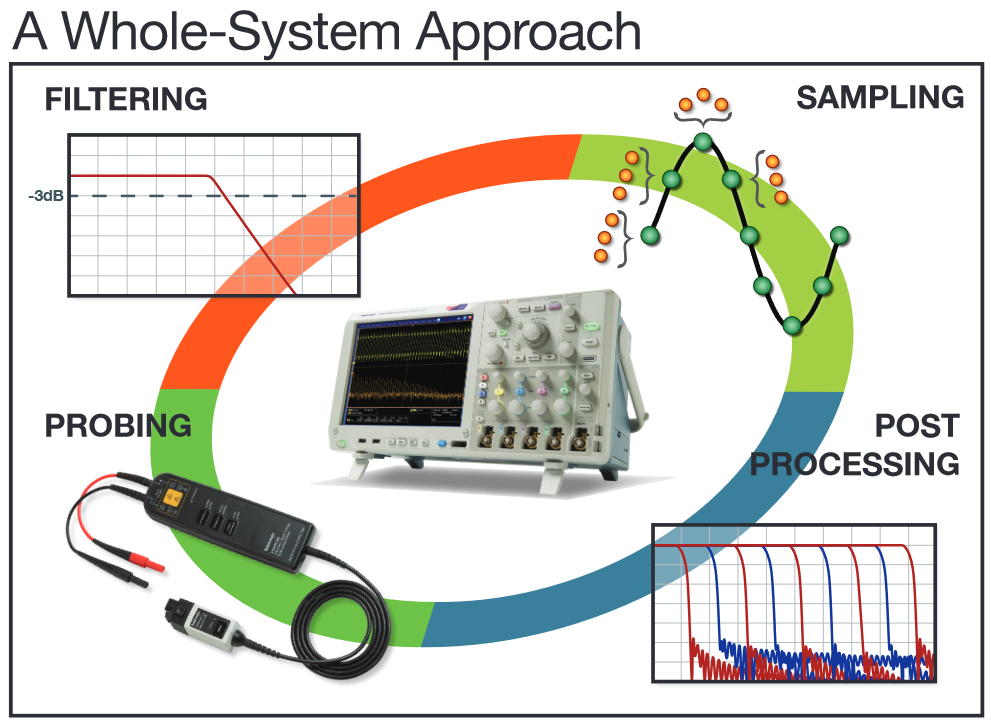
When making high-resolution measurements you can improve your results by looking at your digital oscilloscope as a system. With a basic understanding of oscilloscope operating modes, the performance characteristics of probes, filtering techniques, and how the whole system interacts, you can improve your measurements of small signal details. This application note describes some measurement and signalprocessing techniques that can enhance high-resolution waveform acquisition in modern digital oscilloscopes. Knowing their benefits and trade-offs will enable you to get the best measurement resolution with your oscilloscope.
In order to take high-resolution measurements, it is important to look at the digital oscilloscope as a system -- not simply as an analog-to-digital converter. The whole signal path must be considered - from the probe tip, through the analog front end of the scope, sampling, and digital signal processing. Each of the system elements shown in Figure 1 has an impact on measurement resolution and can be optimized for the best results.
Probing
The Choice of Probes and Probe Settings are Critical
The role of probing may seem obvious, but there are tradeoffs that must be made for optimal results, especially when making high-resolution measurements. The passive probe that was shipped with the oscilloscope may not be the best solution for achieving the best resolution.
For the purposes of this application note, we will give an overview of probing considerations that affect the results of high-resolution measurements. More detailed information on probing is available in the Tektronix ABCs of Probes Primer 60W-6053-XX on www.tektronix.com.
Minimize attenuation to maximize signal to noise ratio.
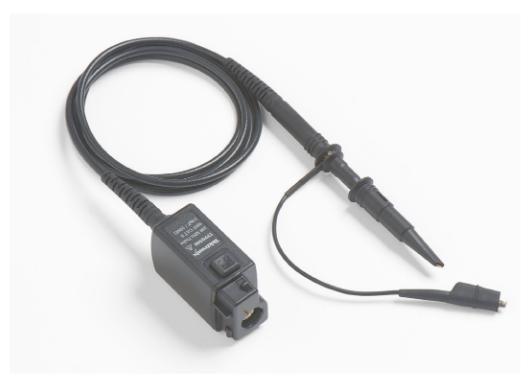
For high-resolution measurements, it is very important to maximize the signal amplitude while minimizing external noise. Probe selection is the first critical step. Voltage probes typically attenuate the input signal by forming a voltage divider (i.e. 1X, 10X, 100X) with the oscilloscope’s input impedance. A 1X probe doesn’t reduce or attenuate the signal, while a 10X probe reduces the input to 1/10th of the original signal amplitude. The oscilloscope compensates for this attenuation by amplifying the signal and, unfortunately, any noise that is added by the probe and the oscilloscope. From a signalto-noise perspective, the optimum probe provides little or no attenuation. For example, the TPP0502 high-impedance passive probe, shown in Figure 2, provides 500 MHz bandwidth but with only 2X attenuation.
Use short leads to minimize noise coupling. All voltage measurements are relative to a reference, often “ground”. Accurate measurements, especially low-voltage measurements, are critically dependent upon a lowimpedance path to the reference voltage. To minimize signal distortion and noise pick-up, you should use the shortest possible grounds. Although the long ground lead on a standard passive probe is convenient for browsing, the lead inductance resonates with the input capacitance, causing ringing on fast edges. A large loop area, formed by the probe tip and ground lead, allows magnetic coupling of noise into the signal. And, close proximity between the inductive reactance of the ground lead and noise sources such as switching devices allows electrostatic coupling of noise into the signal.The best solution is to minimize the length of the ground lead and connect it to a reference point as close as possible to the signal connection.
Reduce noise with built-in probe filters. Many active differential voltage probes and/or current probes come standard with bandwidth filtering capabilities. Bandwidth filtering that’s built into the probe body sometimes provides multiple bandwidth settings for flexibility. In some cases, the probe communicates to the scope when one of these BW filters is selected, which also turns on hardware filtering in the front end of the scope. This further reduces the system noise and contributes to an increased signal-to-noise ratio for the system. Filtering out unwanted noise allows further details to be seen and higher measurement resolution to be obtained.
Measuring Small AC Signals with DC Signals
Note: Whenever large voltages are involved, it is critical for your safety and the equipment’s reliability to verify that the maximum voltages are well within the test system’s “absolute” or “non-destruct” maximum input specifications. In addition, for accurate measurements, it is important that the signals remain within the nominal operating ranges (for example, within an active probe’s linear range or dynamic range).
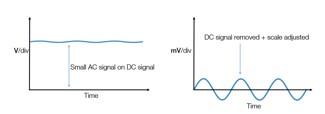
Although low-level measurements near ground are challenging, measurements of low-voltage AC signals riding on large DC components are much more difficult. Making ripple measurements on power supplies is a common example of this application (Figure 6). Dealing with DC offsets can involve probe settings as well as settings on the front end of the scope.
The simplest technique for measuring low voltage signals on a DC offset is to acquire the entire signal with a groundreferenced probe and then attempt to measure the AC component (Figure 3, left). This technique does not allow the AC signal measurements to take full advantage of the measurement system’s dynamic range, and the signal-tonoise ratio will be poor.
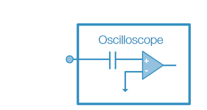
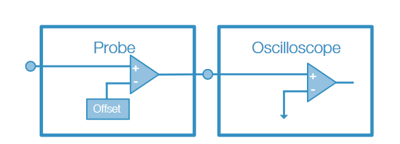
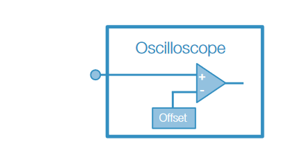

Another technique is to use AC coupling (or “DC block”) at the oscilloscope’s input. AC coupling can usually be selected from the channel settings of the oscilloscope. It blocks DC by inserting a capacitor in series with the input signal. AC coupling works well for removing DC components from the input signal as long as the signal is not being distorted, such as driving an active probe beyond its maximum range. The capacitor is very effective at blocking DC, but may also block very low frequency changes, such as drift. Finally, AC coupling may not be available at all oscilloscope input termination settings.
A better technique is to manually add a precise DC offset voltage at the amplifier to compensate for the DC offset on the input signal. Offset may be applied in the amplifier of an active probe (see Figure 5). Using DC offset is preferable to using AC coupling, since the offset method allows you to see changes in the DC level, whereas AC coupling blocks DC altogether.
Alternately, offset may be applied in the oscilloscope’s input amplifier. Again, this works well for removing DC components from the input signal as long as the signal has not already been distorted.
All of the previous examples have used single-ended or ground-referenced probing. In some cases there may be a component in the circuit that has a low amplitude signal of interest, but the signal is floating at some DC level above or below ground. Rather than using a grounded probe that must measure the DC offset with respect to ground, a better choice may be to use a differential active probe to measure the signal of interest across the component.
For differential probes, all of the guidance about probe specifications still applies, including maximum voltage limits. In addition, Common-mode Rejection Ratio (CMRR) is critical, as it represents the probe’s ability to reject or ignore the DC component of the signal (or any signal that is common to both inputs).
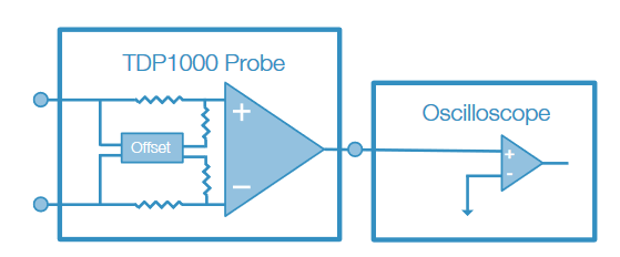
Certain advanced probes, such as the Tektronix TDP1000 differential probe, build on the advantages of differential probing by replacing and improving upon the offset technique with the DC Reject mode. DC Reject automates the offset process by measuring the input signal and generating an internal offset that cancels the DC component of the signal. Because the input signal is always directly coupled to the amplifier, the DC Reject mode does not increase the common and differential mode dynamic ranges for DC components.
Limiting Dynamic Range of Input Signals
To measure detail on the part of a signal around ground, one can scale the waveform up, allowing higher sections of the signal to go off screen. This is a good approach, but you must be aware that overdriving probe or scope input amplifiers can cause distortion unless care is taken. Amplifiers in active probes and in the front ends of oscilloscopes are designed to operate in their linear range. Outside the linear range, the input signals may be distorted. (The linear dynamic range of active probes is typically specified in the data sheet. The linear range for an oscilloscope is approximately full-screen.) When signals exceed the linear range, the amplifiers are over-driven and can take a significant amount of time to recover. This s also called Step Response Settling Time. For example, Tektronix MSO/DPO70000 Series scopes are specified with three parameters: Gain settling (Full Scale), Settling Error (%) and Time. These indicate the specific full scale voltage range, percentage of that range allowed over the screen, and a typical time for the waveform to settle back to normal operations.
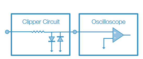
For making high resolution measurements, overdriving the amplifier and exceeding the dynamic range is not generally recommended. However, you may be able to get good measurement results if you are measuring part of the signal that occurs before or well after the overdrive condition, thus allowing the amplifiers to fully recover. Instead of overdriving the scope or probe amplifiers, you should consider using one of the many standard signal clipping circuits found in textbooks and in industry literature. Clipper circuits such as the one shown in Figure 9, are commonly used for limiting the voltage input into a scope. The circuit in Figure 9 would be used to clip the input to one diode drop above or below ground, for more resolution around the point of interest (in this case, the small signal around ground) without overdriving the linear range of the ADC. Similar circuits can be used to offset the area of interest above or below ground.
Filtering
Using Hardware Bandwidth Limiting and Sample Rate to Reduce Noise
In most cases, noise is a bigger factor in making highresolution measurements than ADC resolution. Most oscilloscopes and some advanced probes have a circuit that limits the measurement system bandwidth. By limiting the bandwidth, the noise on the waveform can be reduced, resulting in a cleaner display of the signal and more stable signal measurements. Noise approximately scales as the square root of bandwidth. A side-effect is that, while eliminating noise, the bandwidth limit can also reduce or eliminate high-frequency signal content. Many Tektronix oscilloscopes include 20 MHz and 250 MHz analog filters available in the vertical channel menu.
The sampling rate of a digital scope also factors into noise reduction. The Nyquist Theorem states that in order to reproduce an accurate representation of all signal content within the desired bandwidth, the sample rate must be greater than two times the bandwidth. For example, a 2 GHz channel bandwidth scope will require at least a sample rate over 4 GS/s to accurately represent the signal. Because random noise by definition contains all frequencies, the Power Spectral Density (PSD) of the random noise in the measurement channel is spread equally across the Nyquist bandwidth, half the selected sample rate. For example, on a 5 GS/s oscilloscope the Nyquist bandwidth is 2.5 GHz, but the scope bandwidth at 2 GHz filters noise between the cutoff region and the Nyquist bandwidth, seen in Figure 10.
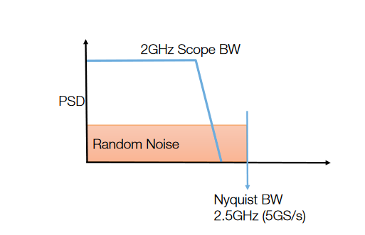
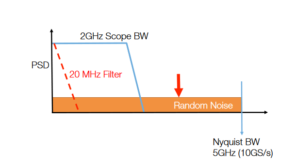
As the sample rate increases, random noise is spread evenly across a wider Nyquist bandwidth range. In Figure 11 we’re looking at a 10 GS/s oscilloscope which has a Nyquist BW of 5 GHz. The random channel noise is now spread over 5 GHz instead of 2.5 GHz. If the oscilloscope bandwidth is kept the same, the net effect is to reject a larger amount of the noise. Using filters to decrease the oscilloscope bandwidth further decreases the noise.
Sampling
Using Sampling Techniques that Boost Resolution
Digital signal processing is commonly applied to raw samples to refine the vertical resolution of an oscilloscope to more than the resolution of its analog-to-digital converter (ADC). Waveform averaging and HiRes are two such processing techniques. Before describing these, it may be helpful to review some definitions.
Vertical Resolution is generally considered a measure of how precisely an Analog-to-Digital Converter (ADC) can convert input voltages into digital values. But more correctly, it is the granularity of the conversion process, and is measured in bits. For example, the vast majority of oscilloscopes are based on 8-bit-resolution ADCs, which represent samples of the input signal as one of 28 or 256 discrete quantization or digitizing levels.
Precision reflects the repeatability or consistency in measuring the amplitude of a signal. Theoretically, the resolution of an N-bit ADC limits the measurement system’s ability to discern and represent a small signal. This ability can be expressed as a signal-to-noise ratio (SNR). The better the SNR the better your chances of measuring small voltage measurements.
SNR = 6.08 * N + 1.8
where: SNR is the signal-to-noise ratio, in dB N is the number of bits in the digitizer
Vertical Accuracy vs. Vertical Resolution
It is important to contrast vertical resolution with vertical accuracy. Vertical accuracy reflects the closeness of an amplitude measurement to the signal’s actual amplitude.
A few digital oscilloscopes have been built with higherresolution ADCs. Although they are implied to be more accurate than 8-bit products, this is not necessarily true. A system with an 8-bit ADC, with high-performance probes and signal processing may deliver results on par with, or even better than a system with a higher bit-count ADC.
DC accuracy is a common oscilloscope specification. It is simply the accuracy with which the instrument can measure a DC value. The implication may be that an instrument with better DC Accuracy will be more accurate when measuring AC signals, but that is not necessarily true. Many other characteristics of the oscilloscopes and probes contribute to the overall accuracy.
A final and much more complex specification is Effective Number of Bits (ENOB), which is a specification of the ability of an instrument to accurately represent signals at various frequencies. ENOB is defined by the IEEE Standard for Digitizing Waveform Recorders (IEEE std. 1057). Like gainbandwidth or Bode plots, ENOB varies with frequency, and generally decreases with frequency. This decline in digitizer performance can be described as an increased random or pseudorandom noise level on the signal. The sources of these errors include DC offset, gain error, analog nonlinearity, converter non-monotonicity and missing codes, trigger jitter, aperture uncertainty (sample time jitter), and random noise. The topic of effective bits is complex and beyond the scope of this document. For further information, please refer to the Tektronix Effective Bits Application Note: 4HW-19448-XX on www.tektronix.com
Oscilloscope Acquisition Modes
In Tektronix oscilloscopes, the term “acquisition modes” refers The default acquisition mode in most oscilloscopes is Sample Mode. This is the simplest acquisition mode, where the typical oscilloscope represents each point on the waveform with an 8-bit magnitude value, at the selected sample rate, up to the maximum sample rate.to the initial representation of waveform data, usually in 8-bit or 16-bit resolution. All subsequent processing operations (display, automated measurements, cursors, math, and applications) are based on the signal representation defined by the acquisition mode.
The default acquisition mode in most oscilloscopes is Sample Mode. This is the simplest acquisition mode, where the typical oscilloscope represents each point on the waveform with an 8-bit magnitude value, at the selected sample rate, up to the maximum sample rate.
For measuring low-voltage signals, two acquisition modes are important, depending on the repeatability of the waveform, since they can be used to improve measurement resolution: averaging and HiRes. These will be covered in detail in the next sections. For information on using other acquisition modes, please refer to the Tektronix XYZs of Oscilloscopes Primer: 03W-8605-XX on www.tektronix.com
Averaging
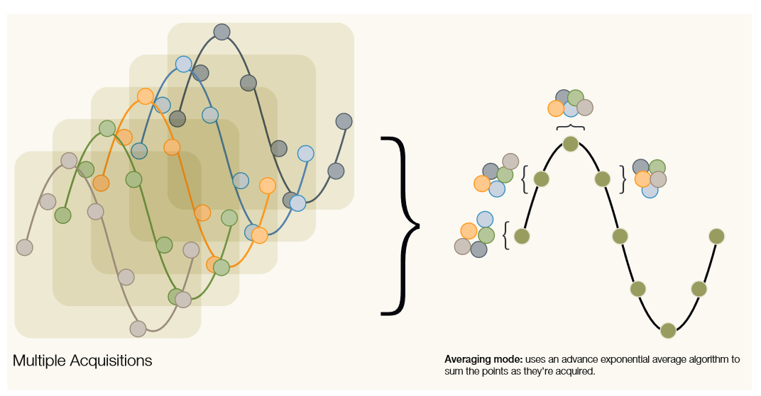
Average mode is one of the basic noise-reduction signal processing techniques in an oscilloscope’s acquisition system. It relies upon multiple triggered acquisitions of a repetitive signal. Using the data from two or more acquisitions, this mode averages the corresponding data points in these acquisitions on a point-by-point basis to form the output waveform. Average mode improves the signal-to-noise ratio, reduces noise that is uncorrelated to the trigger, increases the vertical resolution, and makes viewing of repetitive signals easier.
The conventional method of computing an average waveform is to simply sum corresponding samples from all acquisitions and divide by the number of acquisitions. However, this method would wait until all of the N desired waveforms have been acquired before displaying the average. This delay would be unacceptable to most users, and the volume of acquisition data would quickly overwhelm the oscilloscope’s memory capacity.
AN = (1 / N) * (x0 + x1 + x2 + … + xn-1)
where: AN is a point in the averaged acquisition
N represents the total number of averages requested
xn is a point in acquisition n
n represents the acquisition number
The conventional average algorithm can be modified to display intermediate results each time another waveform is acquired, addressing the delay in displaying the averaged waveform. However, the storage issue for the data remains. The stable averaging algorithm is:
an = (1 / n) * (x0 + x1 + x2 + … + xn-1)
where: an is a point in the current averaged acquisition
xn is a point in the new acquisition n
n represents the acquisition number
Note that, to get a summation average of exactly N acquisitions, simply put the oscilloscope into Single Sequence mode. In this mode, when n reaches N, acquisitions stop and the averaged waveform contains exactly N acquired waveforms.
Tektronix oscilloscopes use an exponential average algorithm, which allows the intermediate results to be updated on the display with each acquisition, and significantly reduces the required storage. The exponential averaging process uses the following equation to create a newly averaged waveform an from a new acquisition xn and the previous average waveform an-1:
an = an-1 + (1/p)*(xn – an-1) = an-1 * ((p – 1) / p) + (xn / p)
where: n represents the acquisition number
N represents the total number of averages requested
an is the new point in the averaged acquisition
an-1 is a point in the past averaged acquisition
xn is a point in the new acquisition
p is the weighting factor
If (n<N) then p = n else p = N
The resulting averaged waveform is the same, independent of which of these averaging algorithms is used. But consider how much more efficient the exponential average algorithm is for both computation and storage of the acquired and averaged waveforms.
Both algorithms readily display the effect of consistent trends in the waveform. You can easily see this with a slow signal. If the signal is stable, you will see a successive reduction of noise during the first N acquisitions. After N acquisitions, the signal will still change, but there will no longer be an improvement in overall noise reduction or vertical resolution.
Averaging increases the vertical resolution of the signal. This enhancement, measured in bits, is a function of the total number of averages:
Enhanced resolution = 0.5 log2(N)
where: N represents the total number of averages requested
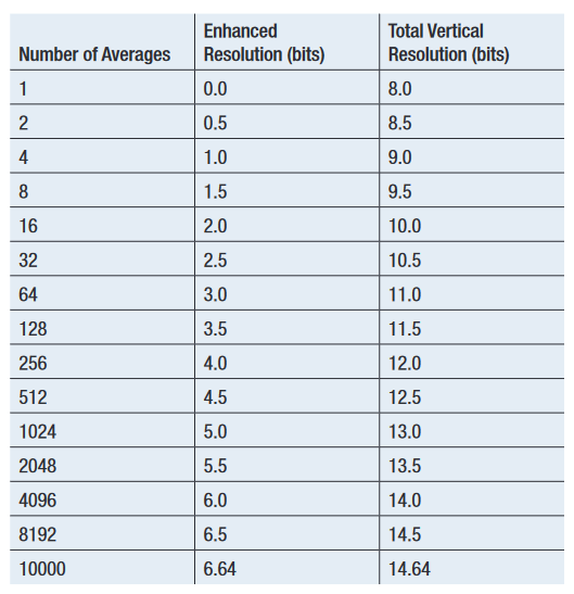
Table 1 shows the ideal resolution enhancement available from waveform averaging.
Again, the values in Table 1 are ideal. In many Tektronix oscilloscopes, the averaging algorithm is implemented with fixed-point math. The maximum number of averages is 10,000, which limits the total bits of resolution to an ideal maximum value of 14.64. In practice, the fixed-point math, noise, and jitter errors reduce the maximum resolution to somewhat less.
HiRes Acquisition Mode
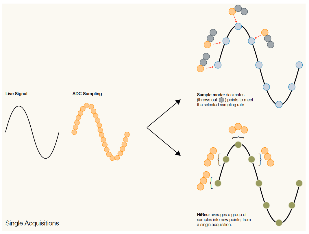
HiRes mode is a Tektronix-patented acquisition process that calculates and displays the average of all sequential sample values in each sample interval. This mode provides a method for trading off over-sampling for additional information about the waveform. In the case of HiRes mode, the additional horizontal sampling information is traded off to provide greater vertical resolution and a reduction of bandwidth and noise. HiRes processing is done in custom hardware to maximize speed. One key advantage of HiRes mode over Average mode is that HiRes mode can be used even on single-shot acquisitions.
The bandwidth limiting and the increase in vertical resolution due to HiRes vary with the maximum sample rate and the actual (selected) sample rate of the instrument. The actual sample rate is typically displayed near the bottom of the screen, and the maximum sample rate can be found in the product data sheet. The bits of vertical resolution is:
Vertical Bits = 8 + 0.5 log2 * (D)
where: D is the decimation ratio, or the maximum sample rate / actual sample rate
The resulting -3 dB bandwidth (unless further limited by the measurement system’s analog bandwidth) is:
BW = 0.44 * SR
where: SR is the actual sample rate
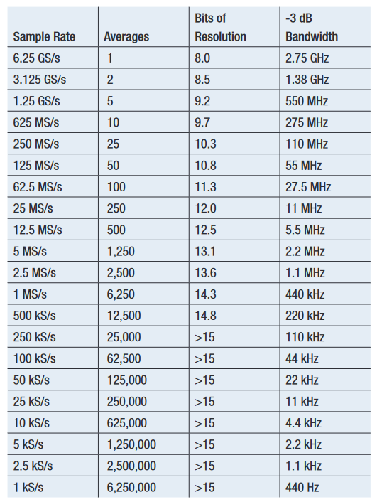
For an oscilloscope, such as the DPO70000 Series, with a maximum non-interleaved sample rate of 6.25 GS/s, HiRes provides the following performance (see Table 2).
For an oscilloscope, such as the MSO/DPO5000 Series, with a maximum non-interleaved sample rate of 5 GS/s, HiRes provides the following performance (see Table 3).
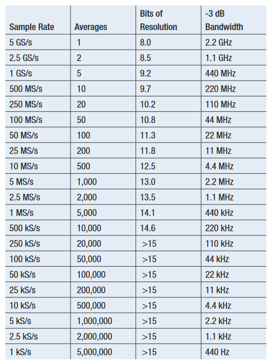
As with averaging, the values in Tables 2 and 3 are ideal. In many Tektronix oscilloscopes, the averaging algorithm is implemented in hardware, with fixed-point math, yielding the maximum resolution value of approximately 16 bits. The observed improvement in resolution may be somewhat less and does vary by application, but this signal processing technique can be extremely valuable for a number of applications.
The examples at the end of this application note demonstrate the technique.
5 Series MSO High Res Acquisition Mode
High Res mode is a new, Tektronix-patented acquisition process that produces very high vertical resolution. At a high level, it is similar to the prior technique, trading off timing resolution for improved vertical resolution by calculating and displaying the box-car average of sequential samples. In addition to the inherent low-pass filtering that occurs with boxcar averaging, a unique FIR smoothing filter is applied to the signal for each sample rate to shape the frequency response and optimize the vertical resolution improvement.
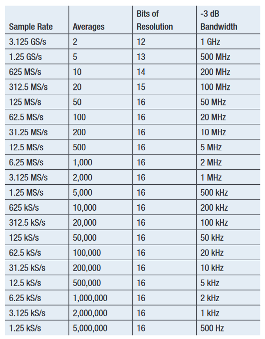
Unlike the prior technique, the 5 Series MSO starts with the output of the 12-bit, 6.25 GS/s ADC and implements the digital signal processing on the ASIC. Also, to improve the user experience, the acquisition badge indicates the number of vertical bits of resolution and the vertical badges for active channels indicate the -3 dB bandwidth.
The High Res acquisition mode in the 5 Series MSO provides the performance shown in Table 4. Note that the bandwidth indicated in Table 4 is further reduced by analog bandwidth limits imposed by the oscilloscope channel and any attached probe

Post-Processing
Noise is everywhere, learn to filter and optimize!
The theme throughout this app note is that measurement resolution can be improved by optimizing all stage of acquisition for improved vertical resolution and noise reduction. Measurement results are dependent on multiple factors and setup conditions. Noise might come from external sources, probing or may even come from the scope itself. While techniques like differential probing, hardware filtering and sampling modes can reduce some of these effects, further enhancements can be achieved by applying user-specified digital signal processing (DSP) filters as well as math channel filtering
Earlier in this application note, analog bandwidth limiting was presented as a technique for reducing broadband noise. Bandwidth limiting is also commonly implemented in software, as are smoothing algorithms, often in combination with hardware bandwidth filtering to help prevent aliasing. Software-based bandwidth limit filters can provide more filter bandwidth selections, better control of frequency and phase response, and sharper cut-off characteristics. Typically these options are found in higher-bandwidth oscilloscopes and available in the vertical channel menu.
Measurement Examples Using Averaging or High Resolution Mode
Small Signal Details with HiRes Mode
This first example shows how the techniques outlined above can be used to overcome the challenge of measuring small signal details in the presence of large signals. These small ripples, voltage variations, are common in power measurements and many other applications. In this example, the output of an electroluminescent (EL Wire) inverter is analyzed. The inverter generates regular bursts in order to drive EL wire used to illuminate different types of devices, toys, clothes, etc. The wire is basically a copper core with a fine copper wire coated in phosphor, and it glows brightly when an AC current passes through it.
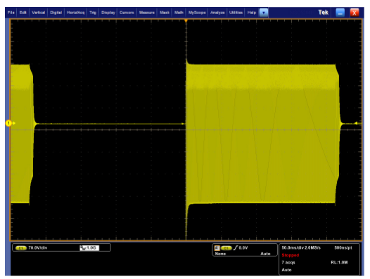
When measuring this specific device one of the burst packets measures 650V peak-to-peak and occurs every 1.7Hz, seen in Figure 15. To capture this signal on an oscilloscope 700V full scale is needed (70V/div * 10 vertical divisions). A typical 8-bit scope can only see 256 digitizing levels (250 across all 10 vertical divisions on a Tektronix scope) which gives a resolution view of only 2.8V per digitizing level. Unfortunately lost in the baseline of the signal is a very low damped signal which has an amplitude of less than a few volts.
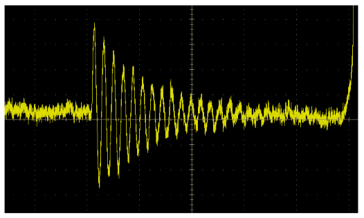
With the help of bandwidth filtering and HiRes mode this scope can be setup to capture up to 11 bits of resolution. Filtering down the noise using both HW filters as well as HiRes mode increases the bits of resolution. As seen in Figure 16, the ringing details have come out of the noise and details can clearly be seen. Now detail down to 30mV is visible!
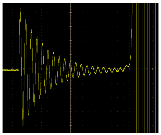
One approach to this signal capture is to double probe the signal with channel one set to 70V/div and another channel set to 1 V/div. The advantage of this approach is the ability to increase the vertical sensitivity to see the desired details with very low noise while ensuring a higher quality measurement. The primary trade-offs in this approach are the use of two scope channels, double probing and ensuring the scope has good overdrive recovery performance. In this case the ringing happens before the overdriven part, so this technique gives good results. As seen in Figure 17, the full details of the ringing can clearly be seen on the overdriven channel.
Measuring 40 MHz Clock Spectrum
The second application is a spectrum analysis of a 40 MHz digital clock. Digital signals transmit most of their information in the time-placement of the edges of the signal (measured where they cross a threshold) rather than signal amplitude. Waveform Averaging is very effective at removing random noise from continuous signals like this.
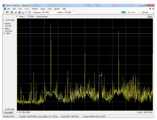
Spectral analysis, partly due to its logarithmic vertical scale, provides a very sensitive measurement of the noise reduction caused by averaging. Notice that the vertical scales in Figures 18 and 19 are 10 dB/div.
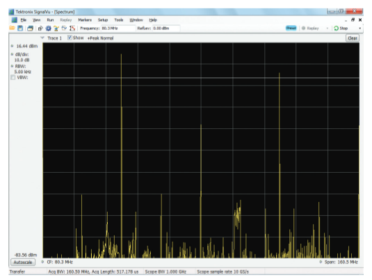
In Figure 19, you can see that the magnitudes of the fundamental and odd harmonics remain fairly constant, but the averaging lowers the baseline noise 10-20 dB, and also lowers many of the other components, making it easier to identify the clock’s harmonics and other interfering signals.
Verifying DAC Resolution
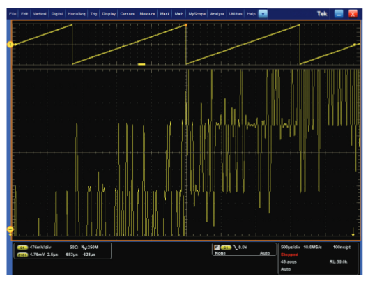
The third example is a method to illustrate the actual vertical resolution improvement using a high-resolution DAC, or, in this case, a high-resolution AWG7000 Arbitrary Waveform Generator. Figure 20 shows a zoomed display of a ramp signal with 10 bits of vertical resolution. Although discrete 8-bit steps can be seen in the lower section of the display, there is sufficient noise on the signal to cause occasional ±1 bit errors. At this 8-bit resolution, those errors are significantly larger than the 10-bit steps on the ramp signal.
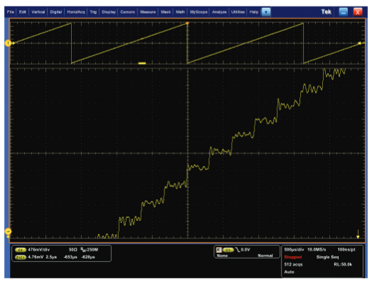
Figure 21 shows the dramatic improvement possible with waveform averaging. In this case, the individual 10-bit steps clearly emerge from the digitizing noise, demonstrating the ability of an 8-bit ADC to provide at least 10 bits of vertical resolution with the help of signal processing such as waveform averaging.
Conclusion
Getting the best measurement resolution involves more than just the number of bits coming out of an oscillscope's ADC. A whole-system approach, from end-to-end is needed to limit the effect of noise, as well as improve digital resolution. This application note has described some of the basic measurement and signal-processing techniques used for high-resolution waveform acquisition in Tektronix digital oscilloscopes and show the benefits with a few simple examples. Knowledge of these benefits and trade-offs will make it easier to choose and successfully apply Tektronix oscilloscopes and probing solutions to make better highresolution measurements.

