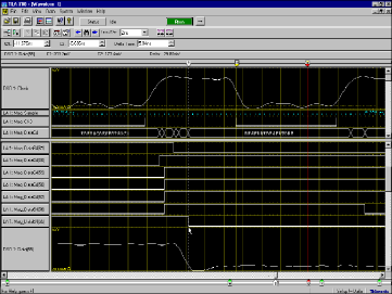
This waveform display of data acquired with MagniVu technology on a TLA 700 Series logic analyzer shows a 64-bit data bus that changes value on the rising edge of the clock. Notice that the bus takes 3.0 ns to settle. The lower traces show several individual data lines in the bus, including the fastest and the slowest. The clock signal and the slowest data line are also shown in analog form using a TLA 700 Series DSO module.

With next-generation microprocessors achieving clock speeds of 200+ MHz and bus speeds breaking the 100 MHz barrier, today's general-purpose logic analyzers are having difficulty providing the timing resolution needed to isolate high-speed glitches or subtle timing problems. 100 MS/s (megasamples/second) synchronous acquisition, typical of today's general-purpose analyzers, is simply too slow to make the 1 to 2 nanosecond (ns) timing measurements needed for next-generation circuits.
Logic analyzer manufacturers have attempted to address this problem by furnishing logic analyzers with a "gear-shifting" option that allows users to tradeoff the number of channels for extra speed if you want twice the acquisition speed, use half the channels; if you want four times the acquisition speed, use only a quarter of the channels. They've also developed special-purpose, higher speed "timing" analyzers specifically designed for timing analysis. But, again, the higher acquisition speeds are achieved only by limiting the number of channels available.
To accurately display a hundred or more channels simultaneously, both of the approaches described above require time consuming re-probing, or double probing which can cause severe probe loading problems and introduce a greater risk of physical damage to the processor or board being tested. Furthermore, while these approaches provide adequate speed for state analysis, they still don't provide the sub-nanosecond resolution needed for accurate timing analysis. Consequently, many circuit designers turn to oscilloscopes when they need to solve timing problems. These timing analysis deficiencies not only extend the design schedule, but also drive up the cost of the overall design effort.
Scaling Up Traditional Logic Analyzer Architecture
The next logical step to achieving higher speeds and greater timing resolution would seem to be simply scaling up existing logic analyzer architecture that is, increasing the speed of the clock and using higher-speed logic. There are, however, inherent difficulties with using the current architecture. In most general-purpose analyzers today, the user's clock (from the circuit being tested) is used to run the analyzer's entire acquisition system log in, triggering, glitch detection, word and range recognition, time stamping, etc. Because it takes time to process this "sample" clock for use by the analyzer, the data being acquired must be delayed, usually through a chain of buffers or delay lines (see Figure 1).

Figure 1. Block diagram of traditional logic analyzer architecture.
Perhaps the biggest challenge in building logic analyzers is ensuring that data delays match the clock delays. Considerable care must be taken to tune the buffers and delay lines so that data and clock are synchronized and channel-to-channel skew among the hundred or more channels is minimized. Conventional logic analyzer designs typically require adding significant delay to the data input paths in order to offset the inherent delays of clock signal processing and to achieve a very low input hold time. (Most customers expect a 0 ns hold time specification.) Any channel-to-channel delay variations make it extremely difficult to achieve the setup-and-hold times required by high-speed circuits. Consequently, simply scaling up current technology to accommodate higher speed circuits only makes the problem of tuning that much more difficult.
In addition, driving the entire system with the user's clock means that the process technology of the analyzer's logic circuits must run at 2 to 4 times the speed of the user's clock. A 100 MHz logic analyzer needs up to 400 MHz logic; a 200 MHz analyzer needs up to 800 MHz speeds that necessitate the use of high-speed BiCMOS or bipolar technology. Scaling up current logic analyzer capabilities by increasing utilization of such high-power/low-density logic, while simultaneously increasing the number of channels to meet the demands of tomorrow's processors, not only increases the space requirements but also becomes cost prohibitive long before the desired timing resolution is reached.
What designers need is a fundamentally new approach that eliminates the need for reprobing and reacquisition when doing state and timing analysis and provides sub-nanosecond timing resolution. Scaling up existing architectures simply isn't cost-effective.
An innovative new approach, created by Tektronix for the TLA 700 Series Logic Analyzers, employs asynchronous digital oversampling technology developed for oscilloscopes to support faster acquisitions across hundreds of channels. The patented MagniVu™ 2 GS/s oversampling architecture provides 500 ps (picosecond) resolution on all 136 channels. And it does so using 250 MHz CMOS logic.
The MagniVu Breakthrough 2 GS/s Acquisitions with a 250 MHz Clock
The high-speed digital sampling circuit for each of the TLA 700 channels consists of a delay chain of eight flip-flops clocked by the analyzer's internal 250 MHz clock, not the user's clock. Each 4 ns tick of the internal clock is used to clock the first flip-flop. The same tick of the clock is delayed 500 ps and then used to clock the second flip-flop; then, 500 ps later, the third flip-flop; and so forth until the eighth flip-flop is clocked and the process starts all over again with the next tick of the clock (see Figure 2).

Figure 2. Oversample circuit diagram.
In other words, each four nanoseconds, eight samples of the data are acquired at 500 ps intervals for each channel. These eight bits of data are then loaded in parallel to a shift register that stores selected data bits to a 512k deep memory. (Selected bits are based on user-defined clocking, triggering, and storage settings.) At the same time, a faster 2k deep memory stores the entire unconditioned stream of data straight from the sampler.
The larger 512k deep main memory stores the overall state activity at up to 250 MS/s asynchronously or 200 MS/s synchronously. The smaller 2k memory, called MagniVu, stores asynchronous data at 2 GS/s, providing 500 ps resolution across all channels and giving designers a clear window into actual signal timing. The MagniVu memory is large enough to store 1 ms of data for each channel or 8 to 20 bus cycles of information for today's leading microprocessors.
Together, the main and MagniVu memories ensure a complete picture of signal activity for both state and timing analysis. Since the state and timing information are derived from the same stream of oversampled data, no reprobing is required to view high-speed data alongside state information. The designer need attach only a single set of probes to view all processor or bus activity.
Advantages of Oversampling

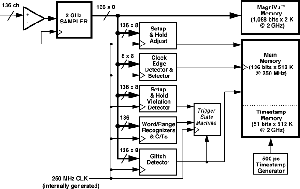
Figure 3. Asynchronous oversampling block architecture.
MagniVu technology allows the TLA 700 Series Logic Analyzers to take on high-speed timing and state analysis tasks other general purpose logic analyzers have, until now, been unable to perform. Digital designers can, for example, use the logic analyzer for timing margin verification, 500 ps time stamping of samples, and improved glitch triggering and storage.
Timing Margin Verification. 500 ps resolution on all channels allows designers to move from simply troubleshooting apparent problems to actually verifying the timing margins of their designs (see Figure 4). Sample points can be moved in 500 ps increments to precisely determine setup-and-hold windows and examine the behavior of clocks, data and address lines with respect to each other, and asynchronous inputs.

Figure 4. 500 ps timing resolution isn't just important to those using leading-edge clock rates. This timing diagram shows the need to verify very short setup time (5 ns) and hold time (3 ns) for a common 33 MHz microprocessor bus.
200 MHz Synchronous Acquisition. The asynchronous digital oversampling architecture enables the TLA 700 to support high-speed synchronous acquisition on all channels. The clock edge detector searches through the oversampled data looking for clock edges that match the clocking setup definition. Based on user-defined setup-and-hold specifications, a specific sample is then selected out of the sampled data stream of all other channels, relative to the timing of the clock edge. The selected samples are then stored, with timestamps, as synchronous data in the primary acquisition memory and all other samples are discarded. This precise sample point placement, together with new high-bandwidth probes, enables the TLA 700 Series to provide 200 MHz state acquisition with a very small setup-and-hold window typically about 2 ns across all channels.
Finely Adjustable Setup-and-Hold Window. Not only does the sample point used for synchronous acquisition dynamically track the actual clock edges, but it can be varied in small increments over a wide range. This allows the user to move the setup-and-hold window to match the specific behavior of the microprocessor or other synchronous circuitry. The window is moved by selecting the desired setup time in the clocking setup window. The setup time can be adjusted from 8.5 ns prior to the clock edge to 7.0 ns after the clock edge in 500 ps increments. The window can also be set independently for any group of channels, providing the flexibility needed for accurately tracking the most sophisticated synchronous designs.
Simultaneous State and Timing Through the Same Probes. Because MagniVu technology acquires high-resolution timing data with each and every acquisition, the designer can see detailed timing simultaneous with state acquisition data. Even if a designer initially specifies only a state acquisition, the detailed timing around the event that caused the trigger can be viewed without having to re-acquire. So when a problem occurs, the crucial details are readily available.
Triggering on Setup-and-Hold Violations. The TLA 700 Series will also trigger when user-specified limits for setup-and-hold time are violated. Some other logic analyzers have the ability to trigger on setup-and-hold violations, but their resolution is measured in increments of several nanoseconds, rendering them useless for high-speed applications.
The setup-and-hold checker detects transitions in input signals during acquisition. The transitions are associated with a clock edge, then any violations are flagged if the transitions are within the interval defined by the user. The setup-and-hold margins can be set independently ±8 ns with respect to the clock edge in 500 ps increments.
500 ps Time Stamping. Asynchronous digital oversampling enables the TLA 700 to generate time stamps every 500 ps. Time stamp values are derived by identifying the precise placement of clock edges in the oversampled data stream of the specified clock channel. The result is exceptionally fine time stamping that cannot be achieved with conventional logic analyzers.
Accurate Glitch Triggering and Storage. With conventional general purpose logic analyzers, high-speed glitch detection has always been an iffy business at best. They can trigger on glitches and perhaps identify the proper channel and the sample during which it occurred. But since the glitch is between samples, the user cannot see what it looks like.
The TLA 700 can hunt for glitches on every channel with a 500 ps glitch detector that monitors the high-speed data stream. When a glitch occurs, the glitch detector triggers the logic analyzer. The designer can then use MagniVu technology to examine the timing characteristics of the glitch and what caused it.
What-You-See-Is-What-You-Triggered-On (WYSIWYTO). The glitch detectors and the setup-and-hold checker monitor the same stream of oversampled data that feeds the MagniVu high-speed memory. Consequently, any timing condition that causes the logic analyzer to trigger is readily viewable in the waveform display, exactly as it occurred when it caused the trigger.
The Next Generation Logic Analyzer
The innovative asynchronous digital oversampling architecture and MagniVu memory of the TLA 700 introduces the next generation in logic analyzer capabilities. By eliminating use of the user's clock and sampling high-speed data directly, and asynchronously, no data delay is required and channel-to-channel delay variations (skew) are minimized. This not only supports the 500 ps resolution needed for accurate timing measurements, but also enables the TLA 700 to achieve the very small setup-and-hold times required for high-speed synchronous state acquisitions. Without having to move a probe or hook up another instrument, the circuit designer can perform both comprehensive timing verification across 136 channels and a complete state analysis.
An Innovative Probing Solution

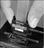
The P6434 high density probe provides convenient connection for 34 channels with an optional latching mechanism and a capacitive loading of only 2 pF per channel. The entire footprint of the connector and latch is only 0.400" × 1.250".
Tektronix has developed an innovative probing solution for the high-density, high-speed circuits of tomorrow. Designed for the TLA 700 Series Logic Analyzers, this high-density probe is a next generation design incorporating a sophisticated mass-termination technology that delivers four times as many connections in the same area as traditional square-pin style probes. Its capacitance is a mere 2 pF, with a controlled impedance environment that minimizes reflections. Each probe wire is coaxially wrapped to provide complete isolation between channels and to shield it from outside interference. The probe also includes an optional latching capability that keeps the connector from accidentally coming loose and ensures a reliable connection.
This high-density probe solution raises probing to the same level of sophistication as today's high-speed processor designs and leading edge TLA 700 Series logic analyzers. With superior electrical characteristics and greater physical flexibility, this probe provides the interface designers need to examine next generation microprocessor designs.

