Introduction
Maintaining the quality and reliability of gate oxides is one of the most critical and challenging tasks in any semiconductor fab. With feature sizes shrinking to 0.18µm or less, gate oxides are often less than 30Å thick. For perspective, the atomic spacing between silicon atoms is 3.1Å, so that a 30Å gate oxide is less than ten atomic layers thick. Vigorous characterization and monitoring is critical for maintaining gate oxide uniformity and quality across an eight-inch or twelve-inch wafer. Further, industry projections over the next few generations of CMOS technology indicate that gate oxides will become even thinner, shrinking to approximately 15Å. This trend signals an urgent need to replace silicon dioxide with gate materials having higher dielectric constants.
Many electrical techniques have been developed over the years to characterize gate dielectric quality. In particular, various current-voltage (I-V) characterization methods have been developed, including the following:
• Time-Dependent Dielectric Breakdown (TDDB), Charge to Breakdown (QBD)
• Tunneling Current (Fowler-Nordheim or Direct Tunneling)
• Stress-Induced Leakage Current (SILC) testing
However, the most commonly used tool for studying gate-oxide quality in detail is the Capacitance-Voltage (C-V) technique. C-V test results offer a wealth of device and process information, including bulk and interface charges and many MOS-device parameters.
|
|
This application note discusses how to use the Keithley Model 4200 Semiconductor Characterization System (4200-SCS) to make C-V measurements. It also addresses basic MOS physics, proper C-V measurement techniques, and parameter extraction from C-V test results. For additional information, refer to the manual for your C-V analyzer and to the 4200-SCS Reference Manual.
Understanding MOS-Capacitor C-V Measurements
C-V measurements are typically made on a capacitor-like device, such as a MOS capacitor (MOS-C). A MOS-C is essentially composed of an oxide that is sandwiched between a semiconductor and a metal/polysilicon gate. The MOS-C can be fabricated directly on the semiconductor substrate or on a p-well or nwell. However, as will be discussed under “Understanding MOS Capacitor C-V Curves,” MOS-C behavior is not as simple as this structure may suggest.
Understanding C-V Measurement Signals
If the MOS-C is fabricated directly on the substrate, the backside of the substrate is used as one of the two electrical contacts needed for a C-V test. See Figure 1.
To measure MOS-C C-V curve, the MOS-C is typically connected to a C-V analyzer, such as the Keithley Model 590 or Agilent 4284A or 4980A. The C-V analyzer applies a high frequency (1MHz or 100kHz) drive signal to the backside of the substrate, via the chuck of a prober. (The prober chuck must be “floating” electrically to avoid diverting the drive signal to ground.) This high frequency AC drive signal is superimposed on a relatively slow DC bias sweep. The signal is picked up through the gate via the manipulator or probe needle.
NOTE If the polarity of the measurement is reversed—the drive signal is applied to the gate via the probe needle, and the signal is measured at the substrate—the additional capacitance of the chuck on which the substrate rests complicates interpretation of the results. Additionally, the chuck acts as an antenna, picking up RF noise from the environment.
Sometimes, as with a MOS-C on a production wafer, the substrate-to-oxide interface is replaced with a well-to-oxide interface. In such cases, a conductor is available at the top of the wafer that connects to the well. The analyzer drive signal is applied to the well through this conductor, and the signal is measured at the gate as usual.
Understanding MOS Capacitor C-V Curves
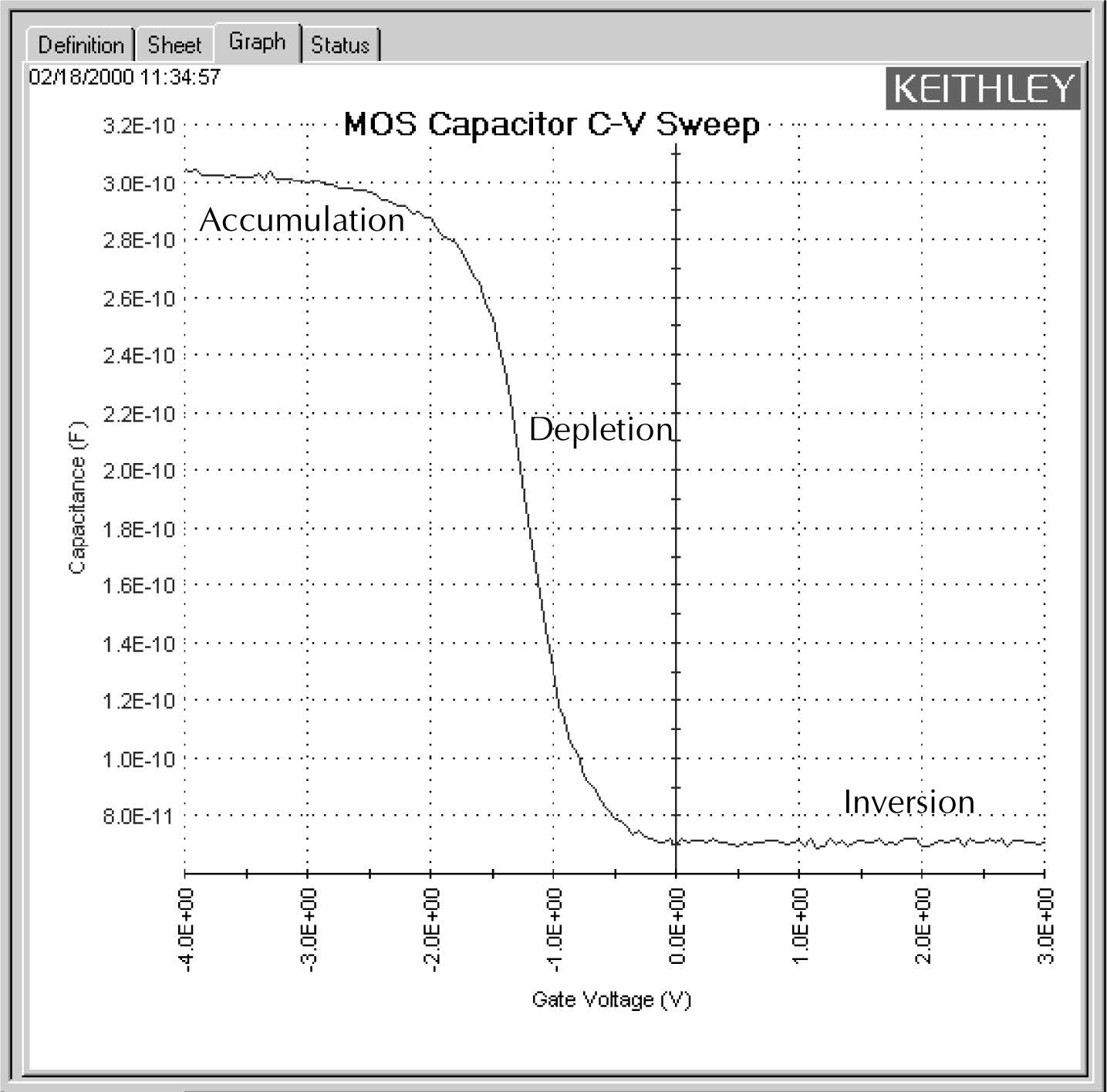
Figure 2 illustrates a high-frequency C-V curve for a p-type semiconductor substrate. A C-V curve can be divided into three regions: accumulation, depletion, and inversion. Each of the three regions is described for a p-type MOS-C.

The C-V curve for an n-type MOS-C is analogous to a p-type, except that 1) the majority carriers are electrons, 2) the n-type MOS-C curve shape is essentially a mirror image of the p-type MOS-C curve shape, 3) the accumulation region occurs at positive polarities, and 4) the inversion region occurs at negative polarities.
Accumulation Region
For a p-type MOS-C, the accumulation region of the C-V curve is observed when negative voltages are applied to the gate. The negative polarity causes majority carriers (holes) to be attracted toward the gate. Because the oxide is a good insulator, these holes accumulate at the substrate-to-oxide/well-to-oxide interface.
A C-V test measures the oxide capacitance in the strong accumulation region—where, for a p-type MOS-C, the voltage is negative enough that the capacitance is essentially constant and the C-V curve slope is essentially flat. There, the oxide thickness can be extracted from the oxide capacitance. However, the C-V curve for a very thin oxide often does not “saturate” to a flat slope. In that case, the measured oxide capacitance differs from the true oxide capacitance.
Depletion Region
For a p-type MOS-C, as the gate voltage moves toward positive values, the MOS-C starts to differ from a parallel-plate capacitor. Roughly at the point where the gate voltage becomes positive, the following occurs:
• The positive gate electrostatically repels holes from the substrate-to-oxide/well-to-oxide interface.
• A carrier-depleted area forms beneath the oxide, creating an insulator. (Recall that the absence of free-moving charges distinguishes an insulator from a conductor.)
As a result, the high-frequency C-V (HF-CV) analyzer measures two capacitances in series: the oxide capacitance and the depletion capacitance. As the gate voltage becomes more positive, the following occurs:
• The depletion zone penetrates more deeply into the semiconductor.
• The depletion capacitance becomes smaller, and, consequently, the total measured capacitance becomes smaller.
Therefore, the C-V curve slope is negative in the depletion region.
Inversion Region
For a p-type MOS-C, as the gate voltage increases beyond the threshold voltage, dynamic carrier generation and recombination1 move toward net carrier generation. The positive gate voltage both generates electron-hole pairs and attracts electrons— the minority carriers—toward the gate. Again, because the oxide is a good insulator, these minority carriers accumulate at the substrate-to-oxide/ well-to-oxide interface. The accumulated minority-carrier layer is called the inversion layer, because the carrier polarity is inverted. Above a certain positive gate voltage, most available minority carriers are in the inversion layer, and further gate-voltage increases do not further deplete the semiconductor. That is, the depletion region reaches a maximum depth.
However, inversion-charge generation is slower than the 1MHz or 100kHz frequency of the HF-CV (High Frequency-CV) measurement. The average time to generate an inversion charge is ≈10τgNa/ni, where τg is the generation lifetime (seconds), Na is the doping concentration (cm–3), and ni is the intrinsic carrier concentration (cm–3). For a 1015 cm–3 doping concentration and microsecond generation lifetime, electron-hole-pair (ehp) generation cannot keep up with the high frequency measurement signal. Therefore, once the depletion region reaches a maximum depth, the capacitance that is measured by the HF-CV analyzer is still based on the majority carrier position and distribution. The following applies:
• The capacitance that is measured by the HF-CV analyzer is the oxide capacitance in series with maximum depletion capacitance. This capacitance is often referred to as minimum capacitance.
• The C-V curve slope almost flat.
NOTE The measured inversion-region capacitance at the maximum depletion depth depends on the measurement frequency. Therefore, C-V curves measured at different frequencies may have different appearances. Generally, such differences are more significant at lower frequencies and less significant at higher frequencies.
Performing MOS-Capacitor C-V Measurements
Understanding Key Requirements for Successful C-V Measurements
Successful measurements require compensating for stray capacitance, recording capacitance values only at equilibrium conditions, and applying and measuring signals in an appropriate sequence. These issues are addressed in the following paragraphs to provide guidance for choosing and/or writing test routines (refer to the next subsection) and preparing for C-V tests.
Compensating for Stray Capacitance
On-wafer C-V measurements are typically performed via a prober (probe station). Signals to multipad test structures are routed between the C-V analyzer and the prober through a switch matrix and interconnecting cables. The cables and switch matrix add stray capacitance to the measurements. However, an integral Keithley Model 590 function can be used to compensate for this stray capacitance. Additionally, a Model 590 offset-cancellation function (ZERO) can be used to eliminate the small offset capacitance that is due to the cables inside the prober and probe card/manipulators. By combining cable compensation and offset correction, the system can be fully compensated from the C-V analyzer to the tip of probe needle, thus ensuring highly accurate capacitance or C-V measurements.
The compensation procedures are summarized below. For more information, refer to the Model 590 Instruction Manual and to Appendix C of the 4200-SCS Reference Manual.
Cable Compensation — The Model 590 provides three different methods to compensate for cable effects. The most common and accurate method uses calibration capacitors. Precisely known capacitance sources (for example, the Keithley Model 5909 calibration sources) are connected in place of the test fixture. These known capacitors are then measured using the Model 590. Thereafter, the nominal and measured values are then compared and cable compensation factors are derived. Four parameters are derived, based on the two-port network model. These four parameters allow compensation for even a complicated path, such as through switch matrix relays.
The 4200-SCS comes with Keithley User Library Tool (KULT) user modules that facilitate cable compensation for the Model 590. The Agilent 4284A, 4980A, and 4294A all use the “open/ short” method to compensate for the cables. The drivers supplied with the Model 4200-SCS assume that the user has performed “open/short” correction from the instrument front panel.
NOTE Cable compensation needs to be performed only after a system configuration change or during a routine metrology calibration.
Offset Cancellation — Before each measurement, a probes-up ZERO (offset cancellation) must be performed. The main purpose of ZERO is to cancel the small residual offset capacitance due to the cables inside the prober and probe card/manipulators. After performing the probes-up ZERO, offset capacitance is subtracted from subsequent measurements. The 4200-SCS comes with KULT user modules that can be used to automate the ZERO process for the Keithley Model 590 C-V Analyzer.
Measuring at Equilibrium Conditions
The most important, but often neglected, C-V measurement requirement is to record data only under equilibrium conditions. A MOS-C takes time to become fully charged after a voltage step is applied. The fully charged condition is generally referred to as the equilibrium condition. Therefore, to allow the MOS-C to reach equilibrium, 1) after initially applying voltage to a MOS-C, allow an adequate hold time before recording the capacitance, and 2) after each step of the MOS-C voltage, allow an adequate delay time before recording the capacitance.
C-V curves swept from different directions may look different. Allowing adequate hold and delay times minimizes such differences.
NOTE One way to determine adequate hold and delay times is to generate a series of C-V curves in both directions. Change the hold and delay times for each pair of inversion → accumulation and accumulation → inversion curves until the curves look essentially the same for both sweep directions.
Hold and Delay Times When Sweeping from Inversion → Accumulation — When the C-V sweep starts in the inversion region and the starting voltage (bias) is first applied, a MOS-C is driven into deep depletion. Thereafter, if the starting voltage is maintained, the initial HF-CV capacitance climbs toward and ultimately stabilizes to Cmin — the minimum capacitance at equilibrium (the specifics of this process depending on the device parameters, such as generation lifetime.) However, if the hold time is too short, the MOS-C cannot adequately recover from deep depletion, and the measured capacitance is smaller than the minimum capacitance at equilibrium.
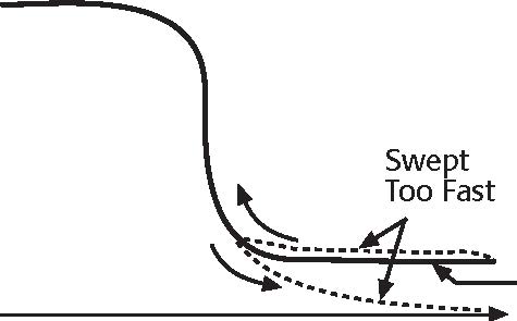
However, once the MOS-C has reached equilibrium after applying the initial bias, an inversion → accumulation C-V curve may be swept with relatively small delay times. This is possible because minority carriers recombine relatively quickly as the gate voltage is reduced. Nonetheless, if the delay time is too short (the sweep is too fast), nonequilibrium occurs, and the capacitance in the inversion region is slightly higher than the equilibrium value. The upper dotted line in Figure 3 illustrates this phenomenon.

Figure 3. Effect of Sweeping a C-V Measurement Too Quickly
Hold and Delay Times When Sweeping from Accumulation → Inversion — When the C-V sweep starts in the accumulation region, the effects of hold and delay time in the accumulation and depletion regions are fairly subtle. However, in the inversion region, if the delay time is too small (the sweep is too fast), the MOS-C does not have enough time to generate minority carriers to form an inversion layer. On the HF-CV curve, the MOSC never achieves equilibrium and eventually becomes deeply depleted. The measured capacitance values fall well below the equilibrium minimum value. The lower dotted line in Figure 3 illustrates this phenomenon.
Using the Preferred Measurement Sequence
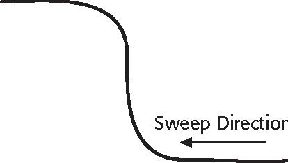
Generating a C-V measurement by sweeping the MOS-C from inversion to accumulation is faster and more controllable than sweeping from accumulation to inversion, for reasons discussed under “Measuring at Equilibrium Conditions.” Figure 4 illustrates the preferred measurement sequence.


The device is first biased for the hold time. The bias voltage should be the same as the sweep start voltage to avoid a sudden voltage change when the sweep starts.
During biasing, if necessary, a short light pulse can be applied to the sample to help generate minority carriers. However, before the sweep starts and before any data is recorded, all lights should be turned off. All measurements should be performed in total darkness, because silicon can be very light-sensitive.
During the sweep, the delay-time parameter should be chosen to optimally balance measurement speed and measurement integrity, which requires adequate equilibration time.
Measuring C-V Curves with the Keithley 4200-SCS
The Keithley 4200-SCS has built-in support for the control of external C-V analyzers. It supports the Keithley 590 C-V Analyzer and the Agilent 4284A, 4294A, and 4980A Precision LCR meters, controlling them via Keithley User Library Tool (KULT) user modules through Keithley Interactive Test Environment (KITE) User Test Modules (UTMs).
Configuring the 4200-SCS for C-V Measurement
Before using a C-V analyzer with the 4200-SCS, system software parameters must be configured to properly recognize the analyzer. For example, to add a Keithley Model 590 to the system,
first start KCON (Keithley Configuration Utility). From the pull-down menu under Tools → Add External Instrument, select Add Capacitance Meter/Keithley 590 CV Analyzer. Next, in the window that appears, set the 590’s GPIB address in the Instrument Properties area. After validating the system, save the configuration. (Use an analogous procedure to add an Agilent 4284A, 4294A, or 4980A.) For more details, refer to Section 7 of the 4200-SCS Reference Manual, “Keithley Configuration Utility (KCON).”
Choosing/Writing C-V User Modules
Before performing C-V measurements, you must choose and/or write KULT user modules to control external C-V analyzers such as the Keithley 590 or the HP 4284A. User modules are written in the C programming language and are compiled and linked using KULT. User modules are then executed in projects by connecting them to KITE UTMs.
Keithley provides several user modules for the most common C-V measurements, including C-V sweep, pulsed C-V, C-t sweep (sampling), and Cmeas (single point) measurements. Supplied user modules are also available for cable compensation. If you need additional C-V user modules, you can write them using KULT. For details about writing user modules and building user libraries, refer to Section 8 of the 4200-SCS Reference Manual, “Keithley User Library Tool (KULT).”
NOTE When selecting and writing C-V user modules, be sure to address the requirements discussed under “Understanding Key Requirements for Successful C-V Measurements.”
Adding C-V Tests to a 4200-SCS Project
After choosing/writing a C-V user module(s), build a KITE test project and create a User Test Module (UTM) for each user module. UTMs can be mixed with Interactive Test Modules (ITM) to perform a sequence of C-V and I-V tests. For example, a tunneling-current I-V measurement can be done first on a MOS-C, followed by a C-V measurement on the same device, and followed thereafter by a breakdown voltage test. With the help of switch-matrix UTM(s) and a switch matrix, such as a Keithley 707A matrix equipped with ultra-low-current 7174A switch cards, these tests can be done automatically in sequence.
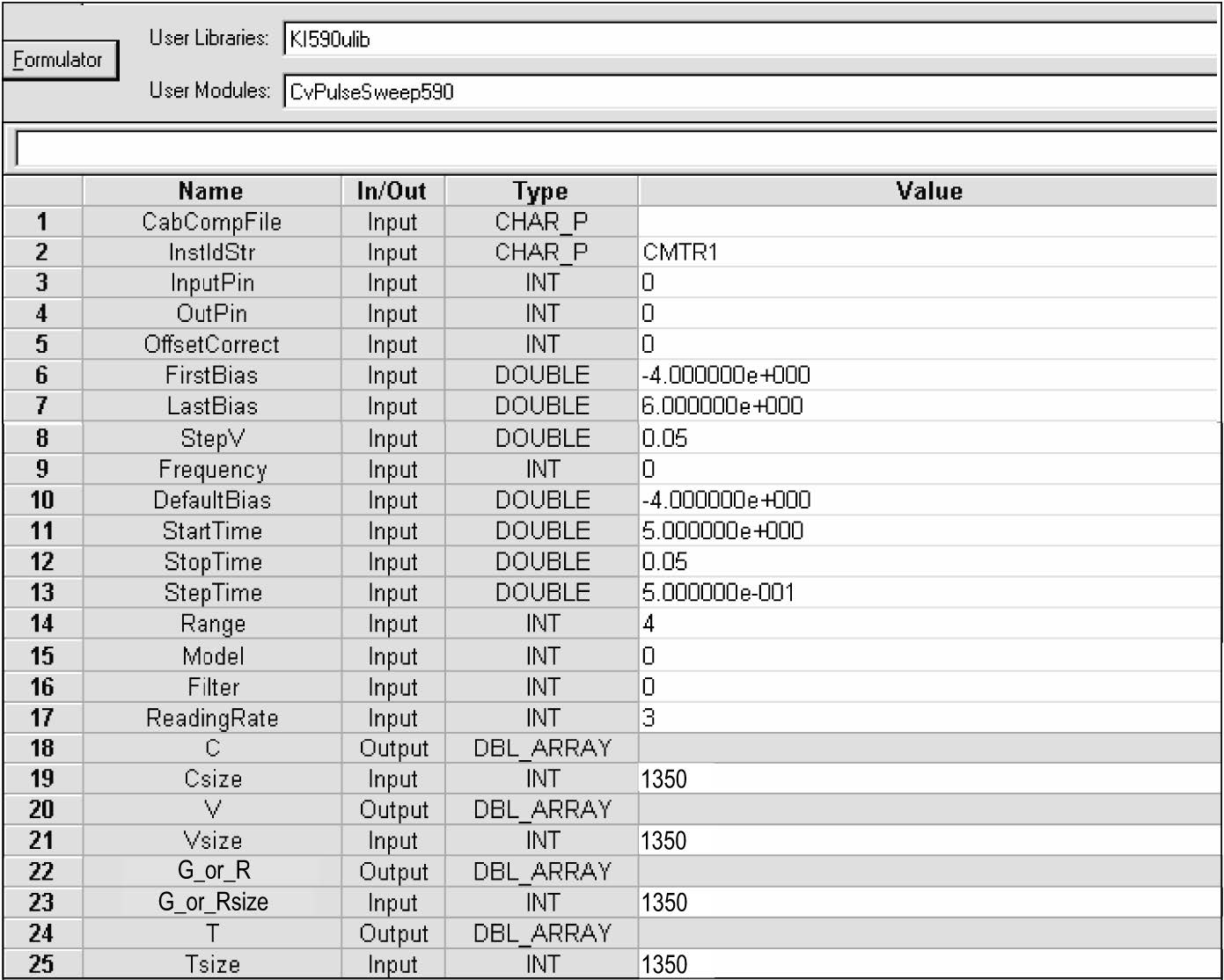
For example, to create a Model 590 CV sweep UTM, do the following: 1) add an unconfigured UTM to the project, 2) in the KITE Project Navigator, double-click the UTM, 3) in the UTM Definition tab that appears, select the KI590ulib User Library and Cvsweep 590 User Module, and 4) type in the measurement parameters such as FirstBias, LastBias, StepV, StepTime, etc. to configure the test. See Figure 5.
Save the project before continuing.

Connecting the C-V Analyzer
Connect a Keithley Model 590 C-V analyzer as shown in Figure 1. Connect an HP 4284A LCR meter as described in Appendix D of the Reference Manual.
Running a C-V Test
Before running a C-V test, ensure that you have performed a probes-up ZERO (offset cancellation) for stray capacitance, as described under “Compensating for Stray Capacitance.” Then, run the C-V test by executing a UTM alone or by executing a project, subsite plan, or device plan containing C-V test UTM(s). For more details, refer to “Executing projects and individual subsite plans, device plans, and tests” in Section 6 of the 4200-SCS Reference Manual.
Compensating C-V Measurements for Series Resistance
After generating a C-V curve, you may need to compensate the measurements for series resistance. The series resistance (RSERIES) can come from either the substrate (well) or the backside of the wafer. For wafers typically produced in fabs, the substrate bulk resistance is fairly small (<10Ω) and has negligible impact on C-V measurements. However, if the backside of the wafer is used as an electrical contact, the series resistance due to oxides can significantly distort a measured C-V curve. This extra series resistance particularly affects HF-CV curves, because the high-frequency capacitance calculations are based on amplitude change and phase shift. The extra series resistance cannot be reduced to a simple two-element (series or parallel) model that the HFCV analyzer can use to calculate capacitance and conductance. However, you can compensate for this series resistance via posttest calculations using the formulas below (Nicollian and Brews p. 224) which are based on the simplified three-element model.


