Introduction
Oxide integrity is an important reliability concern, especially for today’s ULSI MOSFET devices, where oxide thickness has been scaled to a few atomic layers. The JEDEC 35 Standard (EIA/JESD35, Procedure for Wafer-Level Testing of Thin Dielectrics) describes two wafer level test techniques commonly used to monitor oxide integrity: voltage ramp (V-Ramp) and current ramp (J-Ramp). Both techniques provide fast feedback for oxide evaluation.
The instrumentation used to monitor oxide breakdown must provide the following capabilities:
- Accurate voltage and current forcing and measurement capability
- Precise step time control
- Automated device parameter extraction
- Advanced data analysis techniques
This application note describes how to use the Keithley Model 4200-SCS Semiconductor Characterization System to perform oxide reliability testing.
The V-Ramp and J-Ramp Test Techniques
While the V-Ramp test applies a linear voltage ramp, the J-Ramp test applies an increasing logarithmic current ramp until oxide breakdown. The V-Ramp test begins at a low oxide voltage, so it is better able to detect low electric field failures, but it provides poor resolution at high electric fields. The J-Ramp test is different— it starts at a relatively high oxide voltage, so it provides poor low electric field resolution but better resolution at high electric fields. This resolution difference has led to the V-Ramp test often being used to determine infant mortality and low electric field fallout on larger test structures (extrinsic failures), while the J-Ramp test is often used on smaller test structures, where the oxide failure mode is expected to be intrinsic.
The V-Ramp Test Procedure
Figure 1 illustrates the V-Ramp test procedure. The sequence begins with a pre-test to determine initial oxide integrity. During the pre-test, a constant voltage (Vuse) is applied and the oxide leakage current measured. If the oxide is determined to be “good,” a linear voltage ramp is applied to the device until oxide failure. Oxide failure is detected by a sudden increase in current that is ten times the expected value or a measured oxide current that exceeds a specified current compliance. A post-test, which is performed at Vuse, is used to determine the final state of the tested device. Extracted V-Ramp measurement parameters includethe breakdown voltage (VBD) and the charge to breakdown (QBD).

The J-Ramp Test Procedure
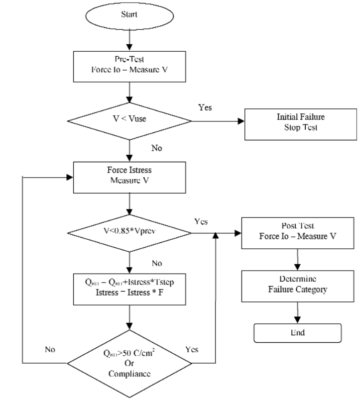
Figure 2 is an overview of the J-Ramp test methodology. The procedure begins with a pre-test to determine oxide integrity. In this pre-test, a constant current (typically 1µA) is applied and the voltage sustained across the oxide measured. If the device is “good,” an increasing logarithmic step current [given by Istress = Iprev * F (where F < 3.2)] is applied until oxide failure. Oxide failure is detected when the voltage across the oxide drops 15% or more from the previous measured voltage (Vprev) or the charge limit is exceeded. A post constant current test is used to assess the final state of the tested device. Extracted J-Ramp oxide breakdown parameters include the breakdown voltage (VBD) and the charge to breakdown (QBD).
Test Difficulties with V-Ramp and J-Ramp
Potential measurement difficulties can arise when implementing either test procedure. The voltage or current step time must be uniform and as precise as possible to determine QBD and VBD accurately. In practice, this step time can be difficult to control because of resolution and accuracy limitations associated with an external controller computer clock. In addition, instrument effects such as range changes can create unpredictable step time variations.
V-Ramp and J-Ramp Using the Keithley 4200-SCS
4200-SCS V-Ramp Test Setup
The Model 4200-SCS’s built-in test sequencer and Interactive Test Module (ITM) capability simplifies implementing the V-Ramp and J-Ramp test algorithms. Figure 3 shows the V-Ramp test sequence in the Project Navigator window and the V-Ramp module Definition Tab. The Project Navigator window displays the test sequence, which begins with a pre-test, followed by a linear voltage ramp (as defined in the V-Ramp module Definition Tab) to oxide breakdown. A post-test determines the final device state.
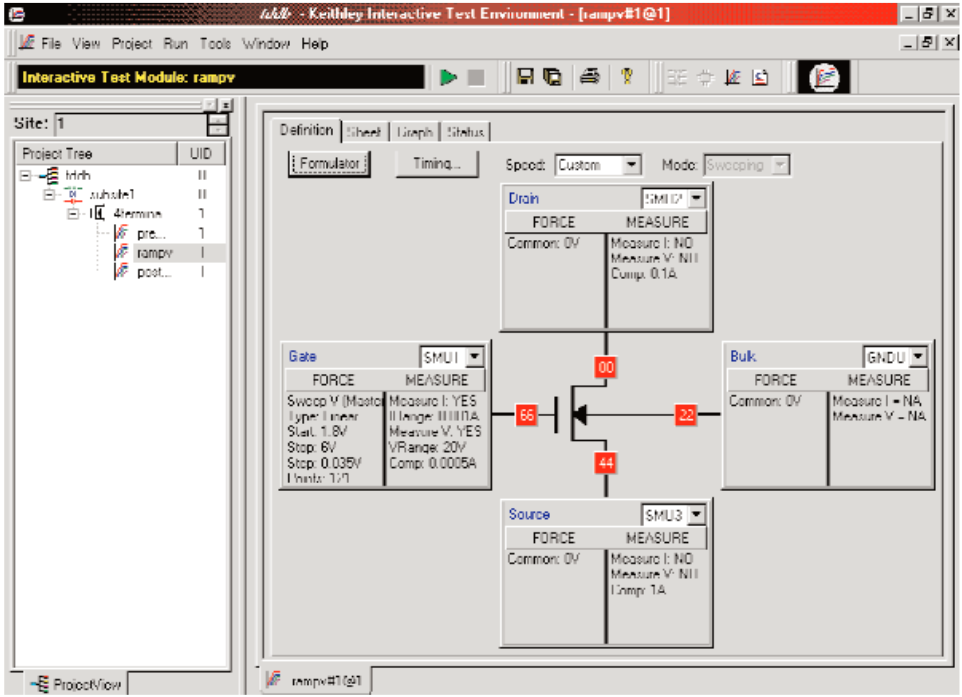
The ITM Definition Tab makes it easy to specify source connections, Force-Measure options, and Timing. In the V-Ramp test illustrated in Figure 3, the Gate source (SMU1) is set for a linear voltage sweep from 1.8V to 6.0V and a voltage step of 0.035V. The voltage step size is based on the JEDEC 35 Standard’s 0.1MV/cm maximum voltage step height requirement (3.5nm oxide thickness). Specifying a fixed voltage source and current measurement ranges minimizes the effect of autoranging on voltage step time.
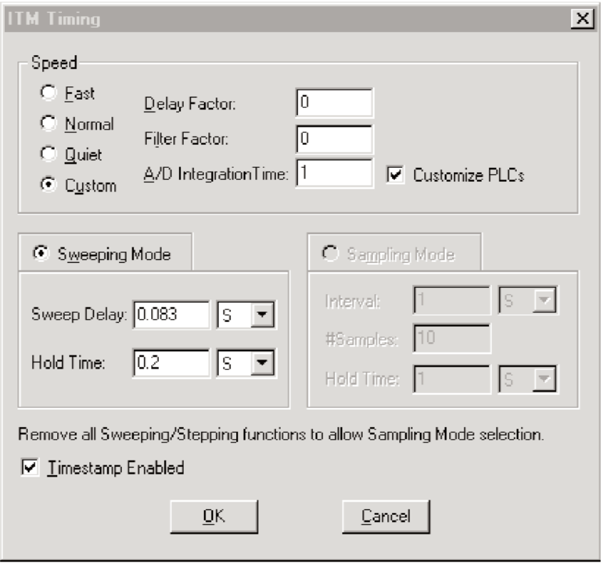
The linear voltage ramp rate is specified in the ITM Timing dialog entry screen (Figure 4), which is opened by clicking the Timing command button shown in Figure 3. SMU measurement time can be precisely controlled by selecting the Custom Speed option and specifying 1PLC A/D Integration Time (16.6ms). The sweep delay is the delay at each step before measurement. In this case, the sweep delay is chosen (83ms) so that the step time is ~100ms (83 + 16.6), yielding a voltage ramp rate of 1MV/cm*s, which is in accord with the JEDEC 35 Standard’s 1MV/cm*s maximum ramp rate requirement. The 0.2s hold time, which occurs on the first voltage step, allows for displacement current settling before the voltage sweep begins. The ITM Timestamp Enabled feature is checked so that precise timing information is saved at each voltage step. This feature is extremely useful when determining QBD and verifying step timing precision. Post analysis of this data showed that voltage step time averaged 99.5ms (expected value 99.6ms) with a standard deviation of ±0.062ms.
4200-SCS V-Ramp Data Analysis
The Model 4200-SCS’s powerful advanced data analysis capability can extract oxide breakdown parameters easily. This analysis feature is activated from the ITM Definition Tab by clicking the Formulator command button (see Figure 3). The Formulator Dialog Entry screen (not shown) contains many functions for data analysis and extraction. A number of Formulator equations are used for automatically extracting the breakdown current (IBD), breakdown voltage (VBD), charge to breakdown (QBD) and time to breakdown (TBD) from the V-Ramp measured gate current (IG) vs. gate voltage (VG) data:
QSUM = INTEG(TIME, IG)
FAILCURRENT = 0.5E-3
COLBD = COND(ABS(IG), ABS(0.98 * FAILCURRENT), 0, 1)
ROWBD = FINDD(COLBD, 1, FIRSTPOS(COLBD)) – 1
IBD = AT(IG, ROWBD)
VBD = AT(VG, ROWBD)
QBD = AT(QSUM, ROWBD)
TBD = AT(TIME, ROWBD)
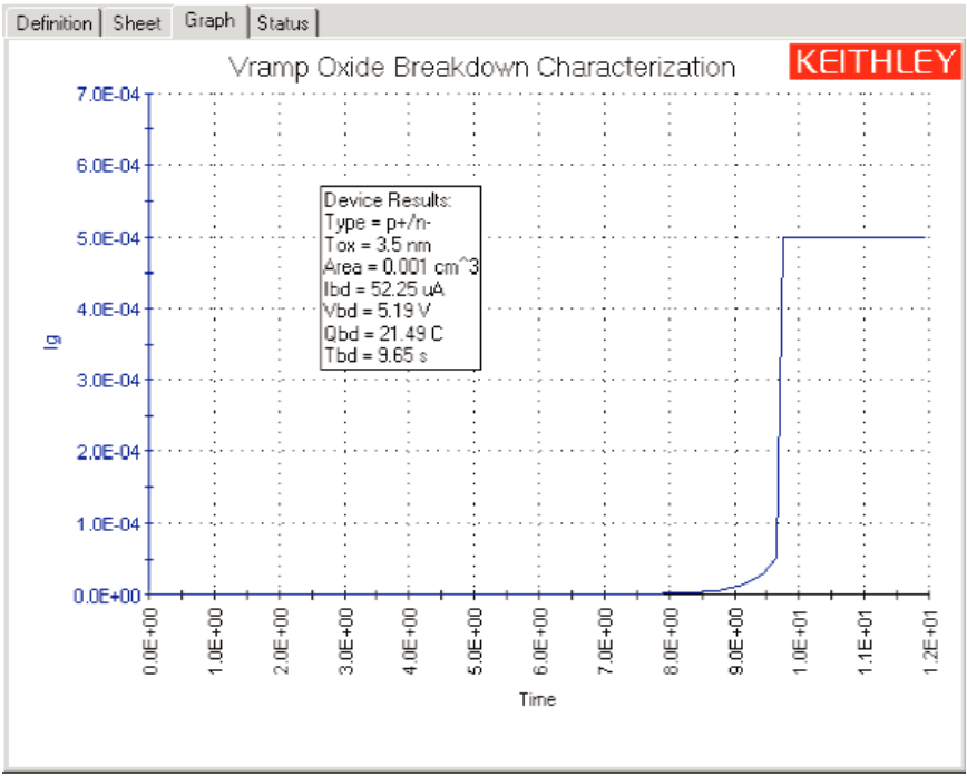
The QSUM equation uses the integrate (INTEG) Formulator function to obtain the oxide charge. The oxide fail current (FAILCURRENT) is specified in the second equation. The equations employing the Conditional (COND) and Find Down (FINDD) functions determine the location of the breakdown row (ROWBD) in the Model 4200-SCS’s built-in spreadsheet, which is compatible with Microsoft® Excel. The ROWBD is used in the AT Formulator function to extract IBD, VBD, QBD and TBD. Once extracted, parameters can be displayed automatically on the Model 4200-SCS’s Graph Tab. Figure 5
4200-SCS J-Ramp Test Setup
Figure 6 shows the J-Ramp test sequence in the Project Navigator window and the J-Ramp test module Definition Tab. The J-Ramp test sequence begins with a pre-test at a constant current to verify initial oxide integrity, followed by a logarithmic current ramp to oxide breakdown. A post-test determines the final device state.
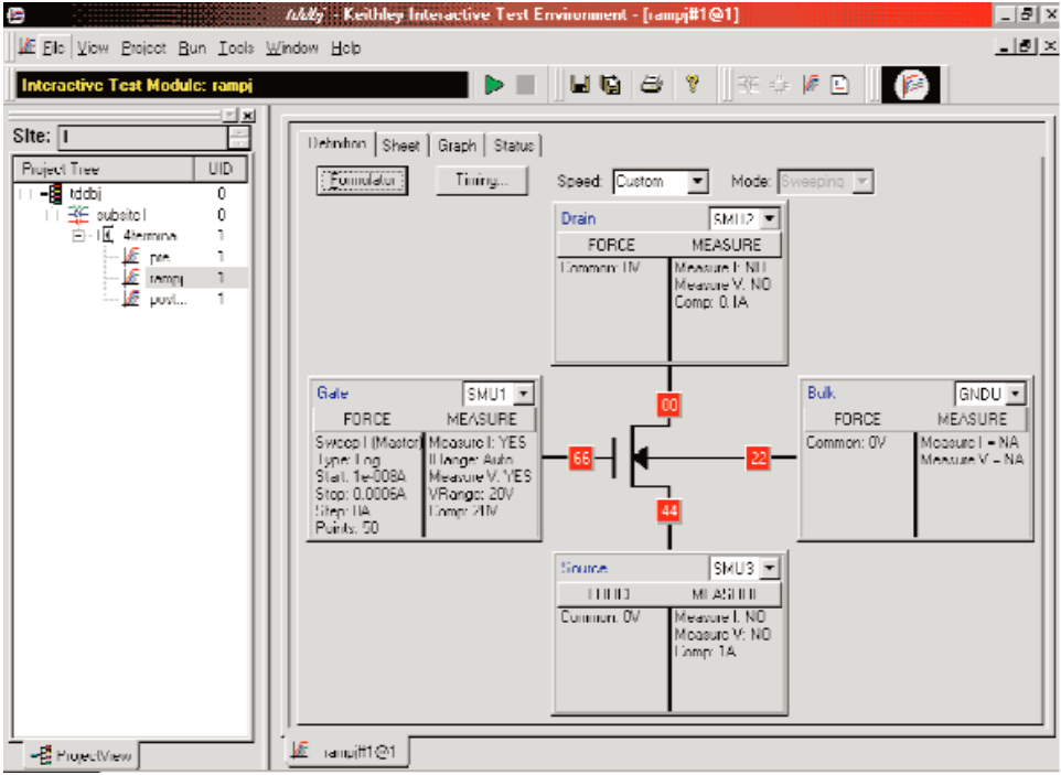
The ITM Definition Tab in Figure 6 specifies J-Ramp test conditions. In this case, the gate source (SMU1) is instructed to perform a logarithmic current sweep from 10nA to 0.6mA, where the number of steps in the current sweep is 50 (F = 1.25). Specifying a fixed voltage measurement range minimizes the effect of autoranging on step time.
4200-SCS J-Ramp Data Analysis
Just as with the V-Ramp test, the Formulator can be used to extract the J-Ramp oxide breakdown parameters (IBD, VBD, QBD, and TBD) automatically. These equations are:
QSUM = INTEG(TIME, IG)
FAILRATIO = 0.85
RATIO = DELTA(VG)/(VG-DELTA(VG))
COLBD = COND(RATIO, FAILRATIO - 1, 0, 1)
ROWBD = FINDD(COLBD, 1, FIRSTPOS(COLBD)) – 1
IBD = AT(IG, ROWBD)
VBD = AT(VG, ROWBD)
QBD = AT(QSUM, ROWBD)
TBD = AT(TIME, ROWBD)
The QSUM equation determines the oxide charge. The second equation specifies the oxide fail ratio (FAILRATIO), which corresponds to a 15% drop in the measured oxide voltage. The RATIO equation determines the ratio of the most recently measured VG to the previous measured value. The next two equations use the COND and FINDD Formulator functions to determine the row location of the breakdown data (ROWBD). The last four equations use the AT Formulator function to extract the breakdown parameters (IBD, VBD, QBD, and TBD) automatically. Figure 7 shows typical Model 4200-SCS J-Ramp data and extracted breakdown parameters for a 3.5nm oxide.

Oxide Defect and Ultra-Thin Oxide Characterization
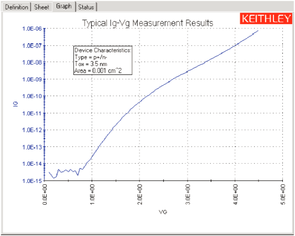
Oxide defects can create excessive tunneling currents at low electric fields. In addition, ultra-thin oxides (<6nm) show substantial direct tunneling oxide currents at low electric fields. To study these effects, it is necessary to monitor oxide currents in the femtoamp range, which makes the Model 4200-SCS an ideal tool for this application. Figure 8 displays typical Model 4200-SCS voltage sweep data on a 3.5nm oxide, which was acquired using the SMU Quiet ITM Timing setting and autorange measurement options. These results demonstrate the Model 4200- SCS’s excellent low current measurement sensitivity.
Conclusion
The Model 4200-SCS’s fast, flexible and easy-to-use test environment provides an ideal approach to characterizing oxide reliability. Its built-in software tools, such as the Project Navigator, the Formulator, and an Excel-compatible data format, greatly simplify creating test sequences and analyzing results. Custom SMU timing controls and advanced Source-Measure Unit technology set a new industry standard for measurement sensitivity, accuracy, and control.
References
EIA/JESD35. JC-14.2 Subcommittee. July 1992. “Procedure for Wafer Level Testing of Thin Dielectrics.”

