연락처
텍트로닉스 담당자와 실시간 상담 6:00am-4:30pm PST에 이용 가능
전화 문의
9:00am-6:00PM KST에 이용 가능
다운로드
매뉴얼, 데이터 시트, 소프트웨어 등을 다운로드할 수 있습니다.
피드백
ONFI Electrical Timing Analysis Solution
TEK-PGY-ONFI software provides complete analysis support for DDR2/3 modes of ONFI Bus. This enables design and test engineers to test ONFI interfaces for compliance to timing parameters of the ONFI Bus specification. This software provides automatic measurements of Command, Address, Data in and Data out transactions. The Detail view feature in TEK-PGY-ONFI software correlates each electrical measurement of the ONFI waveform by annotating with analog waveform making it very easy to debug the timing problems.
Key features
- ONFI Timing measurements and compliance testing per ONFI_4.0, the ONFI Bus specification documentation.
- Supports Timing measurement for SDR, NVDDR, and NVDDR2/3 with limit comparison.
- Detail view allows debugging of ONFI designs by correlating each measurement on the waveform.
- Simultaneous view of DQ and DQS signal provides signal relationship between data and strobe signal.
- Cursors to make timing measurements in eye diagram.
- Immediate result of Eye width and Eye height parameters.
- Ability to store the ONFI Timing measurement results in CSV and txt format.
- Utility features like zoom, undo, and fit screen for easy debugging while correlating the timing measurements to the waveform.
- Report generation using PDF file format.
-
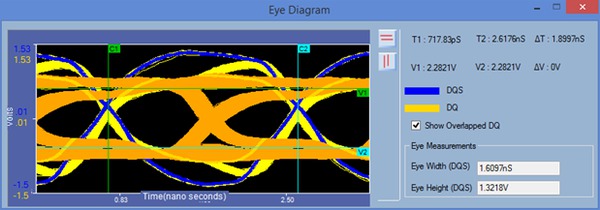
Electrical Eye diagram in TEK-PGY-ONFI software provides quick signal relationship between DQ and DQS signal. Software plots eye diagram for Data-in or Data-out transactions in the acquired waveform. Selected data burst packets waveform is highlighted in blue for easy identification. Horizontal and vertical cursor in eye diagram enables amplitude and timing related measurements.

Electrical Eye diagram showing relationship between DQ and DQS signals
Brief introduction to ONFI
ONFI is a parallel bus. ONFI Bus has control signal, clock and data Signals. To validate timing measurements at high speed (DDR2/3), use the analog channels of the oscilloscope for accurate measurements. Analog channels provide good signal dynamic range and high sample rate. The analog probes provide a good signal fidelity compared to digital channel probes.

DUT of NAND Flash storage device
DQ is shared bus among all NAND flash chips. The control signals such as CE, ALE, CLE, RE, and WE are individual signals.
In this type of DUT, it is important for validation engineers to develop a probing strategy to probe appropriate signals to get accurate measurements. The following approach is recommended to validate this board.
Applications
- Electrical Timing Measurements of ONFI bus
Seamless Integration with Oscilloscope
TEK-PGY-ONFI Electrical Timing Analysis Solution Software runs on Tektronix high performance Windows oscilloscopes. The application automatically imports data from the oscilloscope channels. The application supports .wfm file format for offline analysis. This software package enables live and offline testing of ONFI Signals.

Measurement selections
- Based on the ONFI signals probed using four live analog channels, software will automatically enable the possible timing measurements for these signals
- 45 automated timing measurements as per ONFI standard apart from a few general measurements such as frequency and duty cycle
- Save and recall of application setup for repetitive testing at different times
- Supports single and continuous test mode using oscilloscope live data
Automated Electrical Timing Measurements
Per the TEK-PGY-ONFI specification, the measurement limits are different for each interface and each mode. The TEK-PGY-ONFI measurement algorithms automatically finds the mode and validates with the respective limits. This supports you in identifying the various modes and isolating any compliance issues.
Powerful debug environment: Detail view
TEK-PGY-ONFI software provides two types of debugging capabilities. In one mode, select the worst case result and link directly to waveform as shown here. Software provides the flexibility to define the number of acquisitions and results will include worst case results for all these acquisitions. Software links the worst case results to corresponding waveform acquisition using simple right click of a mouse.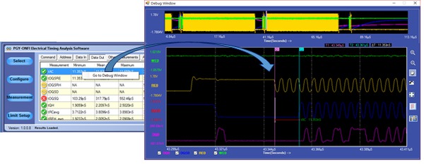
In Detail view debug mode, TEK-PGY-ONFI software displays the last acquisition waveform plot and all electrical timing measurements. Software has the flexibility to display only failed, min and max and all measurement results for available for timing measurements for the acquired waveform. Linking any of the measured results to the waveform helps in debugging the results.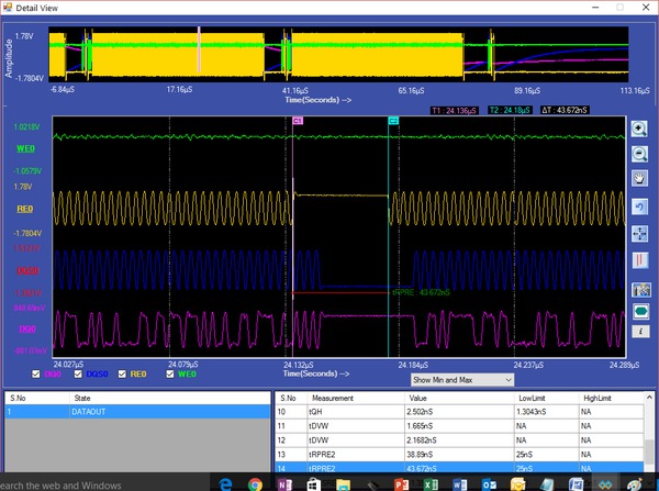
Software displays the eye diagram for correlation DQS and DQ timing relationship. This enables a quick view of any BER during the data-in or data-out operation. It also provides an overall view of total jitter present in DQ and DQS.
Detail view provides following capabilities:
- Plots the acquired waveform in waveform view window
- Lists respective electrical measurements for command, address, data input and data output cycles.
- Zoom, fit to screen, pan, undo, vertical and horizontal cursors enables quick analysis and measurement of electrical signals
Probing challenges and benefits of using Interposers
Silicon package density has driven packages to surface mount ball grid arrays. Data rates are rising, proportionally increasing the need for higher fidelity and signal integrity. If probe points are not designed in, signal access may be poor or not available at all.

Nexus high fidelity interposers are available for standard package types, enabling existing designs to be modified for signal access without compromising the SUTs operation. By using Interposers from Nexus, the problem of signal access while maintaining signal integrity is solved.
Benefits of using Nexus Interposers
- Industry leading interposers are available in different mechanical form factors: socketed for easy interposer or memory removal and replacement, direct attach for use when the target has adequate clearance and a patented edge probe design shown above for extremely tight mechanical requirements.
- When required, interposer designs can be customized enabling interposer solutions for unique customer and SUT requirements.
- Interposer installation can be done by applying readily available BGA rework procedures. Installation services are also available making the rework process simple.
- S-parameter models of the interposer and probe are available for modelling or to generate de-embedding filters to be applied to the oscilloscope,
-
Nexus currently designs interposers for memory technologies exceeding 4267MT/s exceeding today’s Flash requirements.
-
Tektronix offers a complete interposer/probe/scope measurement solution in partnership with Nexus.
Specifications
Category and list of tests supported by ONFI
- SDR Timing Measurements
- Command Latch timing
- Address Latch timing
- Data Input Cycle timing
- Data Output Cycle timing
- Data Output Cycle timing EDO
- Read Status timing
- Read Status enhanced timing
- NV-DDR timing Measurements
- Command cycle timing
- Address cycle timing
- Data Input cycle timing
- Data Output cycle timing
Ordering Information
Recommended configuration
| Equipment | Model | Description |
|---|---|---|
| Oscilloscope | DPO/MSO 70K C/D/DX | Bandwidth 4 GHz and above |
| Probes | P7500 or P7300 | |
| Software | Option TEK-PGY-ONFI | ONFI Electrical Timing Analysis Solution |
| Interposer | NEX-NAND152SCDS | ONFI 152 ball NAND Flash Edge ProbeTM, from Nexus |
| Option | Description |
|---|---|
| TEK-PGY-ONFI | ONFI Electrical Timing Analysis Solution |
| NEX-NAND152SCDS | ONFI 152 ball NAND Flash Edge ProbeTM, from Nexus |

