연락처
텍트로닉스 담당자와 실시간 상담 6:00am-4:30pm PST에 이용 가능
전화
전화 문의
9:00am-6:00PM KST에 이용 가능
다운로드
매뉴얼, 데이터 시트, 소프트웨어 등을 다운로드할 수 있습니다.
피드백
Corus Validation Suite Datasheet
Delivering FPGA-based System On-chip Observability

Features & Benefits
- Very Wide Data Capture Width with Extensive Compression to Optimize Depth
- Time-correlated View across Multiple Clock Domains and across FPGAs
- Any Observed Signal, Any Time, Avoids Frequent FPGA Re-synthesis
- Complex Triggering and Cross-triggering with Test Equipment and Software Debuggers
- Fast and Easy Capture Probe Insertion in FPGAs
Delivering Design-for-Visibility

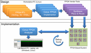
Corus design flow.
Imagine how much faster FPGA system validation and debug would be if you were able to see a time-correlated view of all of your system, not only serial I/O, buses, and software code, but inside the FPGAs as well. The Corus FPGA Systems Validation Suite restores internal visibility by addressing these limitations up-front in the design phase. Corus enables true Design-for-Visibility.
Embedded systems design instruments are fundamental to Design-for-Visibility. Embedded instruments must:
- Scale with technology
- Leverage the same trends that are driving complexity into systems
- Run at speed within the FPGA
- Be scalable across blocks, design, chips, boards, and systems
- Be deployable across the development cycle and into final system
The Corus FPGA Systems Validation Tool Suite is the ideal Design-For-Visibility tool. Corus:
- Produces a system-wide time-correlated view
- Enables observations of large numbers (thousands) of signals
- Delivers “system-time” scale trace depths
- Is implementable across FPGA vendors and ASIC technologies
Corus is a suite of software tools and IP providing everything required to enhance visibility on-chip and off-chip. At the design stage, the easy-to-use Implementor tool applies advanced proprietary algorithms to help you design and implement minimized on-chip signal capture probes quickly and efficiently on your FPGAs.
Implementor Tool

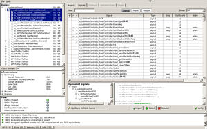
Implementor tool.
- Automatic infrastructure generation
- OptiRank recommends signals for probing
- Automatic clock discovery
- Work from any level of design hierarchy
- FPGA resource utilization summary
- Equivalent signal identification
- Preserves RTL source names

Data compression allows deep trace depths which enables the system to clock cycle-accurate detail with minimal FPGA memory utilization.
During validation, the capture probes are managed by an Analyzer tool through the JTAG port. Complex and cross triggers are easily set up. The Corus “any signal, any time” feature avoids seemingly endless re-synthesis when selecting signals. The resulting highly compressed captures are processed off-chip by proprietary algorithms that recreate the internal chip data and re-synchronize the captures from different clock domains and FPGAs into one view.
Corus can be used with Xilinx, Altera, or Actel FPGAs and requires no special I/O, connectors, or FPGA topology. Simple JTAG connectivity allows full synchronized debug across FPGAs.
Characteristics
| Characteristic | Description |
|---|---|
| Operating System Support | Ubuntu 9 (32 and 64 bit) Ubuntu 10 (32 and 64 bit) Red Hat Enterprise Linux 4 (32 and 64 bit) Red Hat Enterprise Linux 5 (32 and 64 bit) SUSE Linux Enterprise 11 (32 and 64 bit) Windows XP (32 and 64 bit) – Analyzer only |
| Language Support | IEEE 1076-1993/1987 (VHDL) IEEE 1800-2009 (SystemVerilog) IEEE 1364-2001 (Verilog) “Mixed-language” combinations of the above |
| Characteristic | Description |
|---|---|
| JTAG Probes | Altera USB-Blaster All Xilinx JTAG Probes (Xilinx Impact 12.4 or later must be installed) Amontec JTAGKey, JTAGKey2 |
| JTAG TAP Interfaces | Altera TAP Xilinx Virtex-4, Virtex-5, Virtex-6, Spartan-3, Spartan-6 TAPs Actel ProASIC UJTAG TAP Tektronix-supplied JTAG TAP |
| FPGA Synthesis Tools/Flows | Mentor Precision (2010a or later) Synopsys Synplify (2010.09 or later) Xilinx ISE (12.4 or later) Altera Quartus (11.0 or later) Actel Libero SoC (10.0 or later) |
| Characteristic | Description |
|---|---|
| General | - Bit- and word-level compression of trace data before storage (independent per capture station) with potential compression ratios >1000X - Arbitrary signal selection technology and extensive data compression enable effective debug of thousands of signals with as little as 1 dedicated block-RAM - Inter-station cross-triggering between all capture stations including across FPGAs - External trigger-in/trigger-out – requires two dedicated FPGA I/O pins |
| Number of Independent Capture Stations per FPGA | 1 to 255 |
| Number of Instrumented FPGAs per JTAG Chain | 1 to 63 |
| Station Widths (Configurable per capture station) | 16, 32, 64, 128, 256, 512, 1024 |
| Station Storage RAM Sizes (Configurable per station) | 1 Kbits to 8 Mbits |
| Any-Signal-Any-Time Bit-level Signal Selection | Up to 64K signals per station |
| Flexible Instrumentation Options to Allow Lightweight Capture Scenarios | LUT utilization formula: LUT Cost (measured on Virtex-5) ~= 1500 + 3000(m/128) + 4n m = maximum simultaneous observations n = total number of observable signals |
| Characteristic | Description |
|---|---|
| General | - RTL-level naming for VHDL, Verilog, and SystemVerilog during instrumentation - Automatic clock discovery during instrumentation - Automatic assignment of observed signals to clock capture stations during instrumentation - Equivalent signal identification (prevents re-instrumenting of redundant RTL structures) - Hierarchical signal browsing during signal selection in Implementor - GUI or TCL-based Batch mode for Implementor - Implementor project file to enable efficient re-instrumentation of existing RTL - Minimum impact "in-place" modification of original design RTL - Automatic black-boxing of unknown modules - User-controlled black-boxing of modules pre-elaboration (increases runtime performance) |
| Instrumentable RTL Constructs | Input Ports Output Ports Sequential Elements Combinational Signals Base elements of multi-dimensional arrays (all languages) Base elements of complex data types and interfaces (VHDL and SystemVerilog) |
| OptiRank (Design or block level) | State Machine Identification Output Ports Critical Node Identification Critical Node Ranking |
| Automatic Signal Selection during Instrumentation (at any design level) | All inputs All outputs All flip-flops All state bits |
| Import of Signal Selection in Implementor from Existing Formats | Verdi session file DVE session file Plain Text XML |
| Characteristic | Description |
|---|---|
| General | - Time correlation of capture station data across clock domains and FPGAs (single coherent waveform view from all instruments) - GUI or command-line based Batch mode for Analyzer - Analyzer project with unlimited named configurations to store signal selections and triggers - VCD file generation to enable waveform viewing with industry-standard waveform viewers - User-configurable automatic launch of waveform viewer from Analyzer window - RTL-level naming for analysis and data presentation - Hierarchical browsing of signals during signal selection in Analyzer - Automatic real-time frequency detection on a per capture station basis |
| Time-aware Conditional Capture | Continuous mode Windowing mode |
| Local Triggering | Up to 8 equation bits |
| Bus-based Triggering | Up to 32 bits |
Ordering Information
Contact:
Will Shelhamer
Director of Sales, Embedded Instrumentation
Phone: 949.753.5628
Mobile: 760.683.4797
General Enquiries: [email protected]

