Low-power measurements are becoming increasingly important in many line-powered and battery-powered applications, yet many engineers and technicians find it difficult to accurately make these measurements. Although most power measurements simply consist of the mathematical product of the voltage across a device and the current flowing through the device, good low-power measurements require a detailed understanding of oscilloscopes and probing.
This technical brief reviews some of the fundamental performance trade-offs with voltage probes, current probes, and oscilloscopes, and then summarizes with a couple of practical examples.
Optimizing Voltage Probing
Most measurements made with an oscilloscope use a voltage probe, and most users have made many such measurements, so what characteristics of the probes are critical to making good low-power measurements? Here is a brief check-list:
First, remember that all voltage measurements are differential - the measured voltage is always made relative to a reference voltage. The typical passive probe that was supplied with the oscilloscope has a black "ground lead" which is electrically connected to the oscilloscope's ground and should be connected to a ground test point in the device under test. This connection may provide adequate performance for many large-signal measurements, but will typically not work well for low-level signals, since the "ground" is almost never at exactly the same potential as the oscilloscope's ground (because of ground currents in the non-zero impedance between the ground connections). When measuring a voltage relative to a reference point other than ground, a standard voltage probe cannot be used.
Can a pair of passive probes be used to accurately make this non-ground-referenced differential voltage measurement, as shown in Figure 1a? Why not measure the voltage at both nodes and then calculate the voltage difference in the oscilloscope? This method will provide good measurement results only when the probes and the oscilloscope channels are very well matched (gain, offset, delay, and frequency response). This method also doesn't provide very good common mode rejection (nulling out any AC or DC portion of the signal that is common to both inputs). And, if the two signals are not positioned on the display, this technique may not work since you are overdriving the oscilloscope inputs.
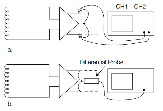
One other alternative to consider is a "floating" oscilloscope, such as the Tektronix TPS2000 or THS3000 Series. Each of the channels of these oscilloscopes is electrically isolated from chassis ground, and when the oscilloscope is powered by its battery, the parasitic capacitance from the oscilloscope chassis to earth ground is also very low. Together, these isolation characteristics of a floating oscilloscope allow the user to make differential measurements with a standard passive probe. This technique can be especially helpful by isolating the oscilloscope power from a noisy ground environment.
For the best measurement quality and ease-of-use with a standard oscilloscope, an active differential probe (such as the Tektronix TDP1500 or TDP1000) is strongly recommended for making milliVolt-level differential voltage measurements, as shown in Figure 1b. For making microVolt-level differential voltage measurements, a differential preamplifier (such as the Tektronix ADA400A) is the best solution.
Second, consider the effects that the probe’s impedance or loading will have on the circuit under test, as shown in Figure 2. Ideally, the impedance at the probe tip would be infinite at all frequencies. In practice, the input resistance is often in the MegOhm range, but the input capacitive reactance XC is:
XC = 1 / (2 * PI * f * C)
where the f is the frequency in Hertz and the C is the capacitance in Farads
so a 1 pF capacitance has an impedance of only 160 Ohms at 1 GHz! (Some higher-performance probes include some resistance in series with the input capacitance to maximize the high-frequency capacitive reactance, as can be seen in the typical impedance vs. frequency plots in the probe data sheets.)
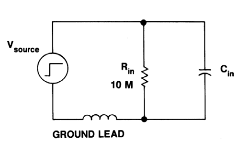
Adding accessories to the probe tip also affect the input impedance, increasing input capacitance and adding series inductance.
Remember, for good measurement accuracy, the probe's input impedance should be much greater than the circuit's impedance at the highest frequency of interest.
Third, don't use more probe attenuation than needed to match the signal amplitude to the dynamic range of the oscilloscope input. The typical "10X" passive probe has an attenuation factor of 10, which means that only 1/10th of the input signal amplitude is applied to the oscilloscope. Although this probe attenuation extends the maximum voltage range of the measurement system, it has the unfortunate side effect of reducing the signal-to-noise ratio (SNR) for small signals (when the oscilloscope gain is increased to compensate for the probe attenuation):
SNR = Vinput / (probe attenuation * Vnoise)
where Vnoise is the measurement system's noise referred to the oscilloscope input
Fourth, don't use more probe bandwidth (or faster rise-time) than the application really requires. Good measurement technique suggests that the bandwidth of the measurement system (probe plus oscilloscope) should be at least five times the highest frequency of interest for <3% amplitude error, or the system rise-time should be less than one fifth of the fastest rise-time of the signal being measured for <2% rise-time error. (It is wise to observe the signal with full bandwidth to verify the highest frequency of interest before adjusting the bandwidth.)
However, excessive measurement bandwidth increases the bandwidth of captured noise, which degrades the SNR. If the probe has a bandwidth control, use the lowestbandwidth setting consistent with good measurement technique. If the probe does not have a bandwidth control, decrease the bandwidth setting in the oscilloscope, again consistent with good measurement technique.

Fifth, remove any residual DC offset in the measurement system (manually or automatically) before making any measurements, preferably in the probe, so the offset is removed from all oscilloscope measurements. To remove the DC offset, some probes allow the user to add an offset signal, while other probes provide AC coupling to attenuate low-frequency signal components. DC Reject, an automatically-generated DC offset capability is another very convenient capability for handling offsets.
Although a 1 mV DC offset may be negligible for measurements of over a Volt, such an offset represents an intolerable 10% error for a 10 mV measurement. And, since instantaneous power is the product of a voltage and a current, a DC offset will cause an error in the calculated power, either inflating the value or possibly even changing the polarity of the calculated value.
Sixth, minimize probe lead lengths to minimize the ringing on the signals. As shown in Figure 3, the inductance of the probe leads form a resonant circuit with the probe’s input capacitance and will cause ringing after fast edges in the signal at a frequency specified by:
f = 1 / (2 * PI * SQRT(L * C))
where f is the frequency in Hertz, L is the probe's lead inductance in Henrys, and C is the probe's input capacitance in Farads
For example, Figure 3b shows that the long probe ground lead is resonating with the probe's input capacitance and ringing at about 33 MHz, well within the bandwidth of the measurement system.
The impact due to ringing can be minimized by decreasing the lead inductance (and/or probe input capacitance) until the ringing frequency falls above the measurement system's bandwidth.
Seventh, minimize the area of the loop formed by the probe leads. By minimizing the loop area (for example, by twisting the leads together), the magnetic coupling of noise into the probe is minimized.
And, keeping both leads equidistant from electrical noise sources, so the capacitive coupling of noise into only one of the probe leads is also minimized. When measuring signals in high-radiated-noise environments, twist the differential probe leads together. That way, any electrostatic coupling of noise will tend to appear as a common-mode signal, which can be rejected by the differential amplifier.
Finally, connect both voltage probe inputs as close as possible to the desired test points in the circuit. Especially for low-voltage measurements, even small voltage drops across circuit board traces and connectors can significantly affect amplitude measurements, and the parasitic inductances and capacitances in the circuit can affect the frequency response of the signals.
As component sizes shrink and circuit board technology allows more blind and buried connections and components, a product's design-for-test requirements need to include probe access to critical signal nodes and near-by grounds. This access can include individual pins, circuit board pads, or circuit board vias without solder mask.
Optimizing Current Probing
There are a variety of techniques that can be used to measure the current flowing through a device. Each has advantages and disadvantages. So which currentmeasurement techniques are most appropriate for low-current measurements? Here is a list of common alternatives:
The simplest current measurement technique is to measure the differential voltage drop across a resistor that is already in the design. A low-resistance sense ("shunt") resistor can also be added to the circuit (with the probe’s input impedance in parallel) and the differential voltage drop can be measured. However, there are some significant limitations to this method:
- Measuring the differential voltage drop across the sense resistor with an active differential probe will provide the best results, as long as the common-mode signal is within the probe’s specified operating range. However, this technique will often be sensitive to ambient noise. The effects of the noise can be minimized by minimizing probe attenuation and bandwidth, as described in the Voltage Probing section.
- If a sense resistor is added to the circuit, there is a serious compromise to be made. As the resistance value increases, the SNR improves, but the power dissipation in the resistor increases and the additional voltage drop can cause the circuit behavior to change. Many highpower resistors such as wire-wound resistors also add inductive reactance to the circuit. And, don’t forget that the differential probe input capacitance appears in parallel with the sense resistor, forming an RC filter.
- If you do add a sense resistor to the circuit, try to add it as close to ground as possible to minimize the commonmode signals across the resistor that the measurement system must reject. And, unlike high-performance current probes, the common-mode rejection performance of differential voltage measurements tends to fall off over frequency, reducing the accuracy of high-frequency current measurements with sense resistors.
For low-frequency measurements of low current levels, a transimpedance amplifier can also be used. Instead of measuring the voltage drop across a sense resistor, the current flowing into the amplifier input node (which is at virtual ground) is measured, reducing the offset voltage error. This is the technique used in the Tektronix DMM4020 digital multimeter to make nanoAmpere measurements.
For AC-only, low-amplitude current measurements, very small current transformers (for example, the Tektronix CT1 or CT6) may be the best choice. Because the devices are small, a short wire or a component lead will fit through the hole in the device, enabling the measurement of the current on the wire, as shown in Figure 4. However, because the device is a transformer, there are low- and high-frequency limits on the bandwidth, and the maximum current level is limited by core saturation in the transformer.
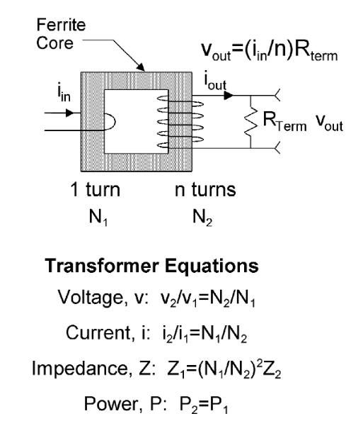
For many applications, a split-core, AC/DC current probe (for example, the Tektronix TCP0030) is the most accurate and easy-to-use solution. AC/DC current probes use a transformer to measure AC currents and a Hall Effect device to measure DC current. Split-core probes allow the transformer in the probe head to mechanically open and then close around the conductor.
Because an AC/DC current probe head must encircle a conductor, it is wise to consider adding current probe access to a product’s design-for-test requirements. This access can include individual current-carrying cables or a circuit board cut-out around a current-carrying trace.
As with any complex measurement device, there are some performance characteristics to consider when using an AC/ DC current probe. Here is a brief check-list:
- First, the current probe head must be connected around the current-carrying conductor being measured. If an individual wire of sufficient length is available, the probe can be connected around it. On a circuit board, it may be necessary to add a wire loop or tip up a component and add a wire in series to accommodate the probe head.
- Second, consider the inductive insertion impedance that is added to the circuit. A typical current probe may add a few nanoHenries of inductance, but the total inserted inductive reactance is probably dominated by the inductance of the wire (about 20 nH / inch) added to accommodate the current probe.
Third, be careful when orienting the wire loop and probe over the circuit because the resulting loop area may be significantly larger than the connection in the original circuit, making the circuit more susceptible to magnetic coupling of noise.
- Fourth, consider the parasitic capacitances between the conductor and the current probe body and between the current probe body and ground. Fast slew-rate voltage signals can be capacitively coupled into the probe body. Whenever possible, probe on the lowest-impedance nodes to minimize the loading effects of capacitive coupling to ground. Also, probing on the grounded side of the circuit will minimize the signal's slew rate (dV/dt) driving the parasitic capacitance.
- Fifth, as with voltage probes, don't use more attenuation in the current probe than is necessary to match the signal amplitude to the dynamic range of the oscilloscope input. The less-sensitive scales allow for the capture of higher peak currents, but they also degrade the SNR for small signals. So, the best measurement results are achieved when the probe scale is as sensitive as possible without clipping the peaks on the current waveform.
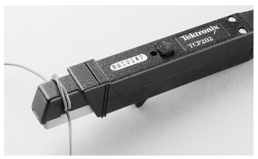
- Sixth, because current probes respond to the total current flowing through them, the measurement sensitivity can be improved by wrapping multiple turns of the conductor around the current probe, as shown in Figure 5. If the conductor goes through the current sensor N times, the sensitivity is increased by a factor of N. The actual current value is then determined by dividing the total measured amplitude by N. NOTE: Winding more turns around the probe increases the insertion impedance (inductance rises at the square of the turns) and reduces the upper bandwidth limit of the probe.
- Seventh, to reduce the susceptibility of the probe to radiated noise, try connecting a probe ground lead from the ground connection on the current probe to the circuit ground. This may increase the parasitic capacitance from the probe head to ground, but it should make the probe’s internal shielding more effective.
- Eighth, don't use more measurement system bandwidth (or faster rise time) than needed for the measurement. In general, the current probe's sensitivity is limited by the SNR of the entire measurement system. For example, the Tektronix TCP0030 is the most sensitive AC/DC probe available, specifying a 1 mA/div sensitivity, limited by overall measurement system noise. This sensitivity can be improved by noise reduction signal processing in the oscilloscope with techniques such as waveform averaging, HiRes, and bandwidth limiting.
- Finally, allow the measurement system to warm up for several minutes and then degauss (to remove residual magnetic flux) and remove DC offset (manually or automatically). Temporarily disconnect the probe from the circuit or de-energize the circuit while degaussing and removing DC offset from the probe.
For further technical information on oscilloscope probes, please refer to the Tektronix ABCs of Probes Primer 60W-6053-XX on www.tektronix.com.
Optimizing Oscilloscope Setup
The oscilloscope setup is the final step in optimizing the measurement system for low-power measurements. Here is a brief check-list:
First, accurate measurements always begin with a calibrated oscilloscope. Allow the oscilloscope to warm up for at least 20 minutes to reach a stable internal temperature. The majority of short-term errors are caused by amplifier drift over time and temperature. It is highly recommended that the oscilloscope be calibrated before making critical measurements, when the ambient temperature has changed more than 5 degrees Celsius, and at least once a month. With many oscilloscopes, this calibration is automated and takes just a few minutes to complete. (For example, on the Tektronix Windows-based oscilloscopes, this calibration feature is called Signal Path Compensation (SPC) and is found in the Utilities- >Instrument Calibration… menu. Just follow the on-screen directions.)
Second, as with the voltage and current probing, optimize the dynamic range of all of the signals. If necessary, use AC coupling to remove unwanted DC offset from the signal. Adjust the coarse and fine vertical scale controls so that the signals fill most of the display vertically, but that the peaks do not extend beyond the top or bottom of the display. This adjustment uses the lowest necessary attenuation settings and optimizes the SNR.
Third, adjust the trigger level to stabilize the display. Simply selecting edge trigger and setting the trigger level near the center of the waveform is sufficient.
Fourth, adjust the horizontal scale control to capture the desired time window.
Fifth, adjust the sample rate to accurately represent the signals and prevent aliasing. A good rule is to set the sample rate at 20-25 times the highest frequency of interest. This sample rate supports a single-shot bandwidth of about five times the highest frequency of interest, assuming the oscilloscope uses sin(x)/x interpolation.
NOTE: The time window, sample rate, and record length settings are inter-related according to the following equation:
T = RL / SR
where T is the time window (in seconds), SR is the sample rate (in samples/second), and RL is the record length (in samples) So, as the sample rate is increased, the record length will also need to be increased proportionally to keep the time window constant.
However, as discussed in the probing sections, don’t use more bandwidth than you really need, because unnecessary measurement bandwidth increases the bandwidth of captured noise, which degrades the SNR. Use the bandwidth limits in the oscilloscope or the probe to optimize the SNR for the signal of interest.
Sixth, deskew the probes. Each probe has a different propagation delay, and the differences can be dramatic especially when comparing voltage and current probes. Because the instantaneous power calculation is the sample-by-sample product of the voltage and current waveforms, precise time (phase) matching of the waveforms is required. The deskew process time-aligns the signals at the oscilloscope inputs, assuring the calculated power waveform represents the circuit’s true instantaneous power.


Seventh, use the oscilloscope's signal conditioning to remove unwanted, random noise. There are two signal processing techniques to consider:
The first is waveform averaging, shown in Figure 6, which averages corresponding samples from subsequent triggered acquisition. This technique does require a repetitive signal, but provides very effective removal of random noise. And, if the sample rate is very high compared to the frequencies of interest, the effective system bandwidth is not affected. Finally, waveform averaging increases the vertical resolution of the sampled waveform:
Enhanced resolution = 0.5 log2(N)
where N represents the total number of waveform averages
The second technique is HiRes, shown in Figure 7, which is a form of boxcar averaging. This technique averages a group of successive samples within an acquisition. As such, this technique will work with single-shot events, and is effective at removing random noise.
As with waveform averaging, HiRes increases the vertical resolution of the waveforms:
Enhanced resolution = 0.5 log2 * (D)
where D is the decimation ratio, or the maximum sample rate / actual sample rate
A side benefit of HiRes is that the effective system bandwidth is predictably reduced, helping to limit the noise bandwidth of the system. The resulting -3 dB bandwidth (unless further limited by the measurement system’s analog bandwidth) is:
BW = 0.44 * SR
where BW is the bandwidth (in Hertz) and SR is the actual sample rate in (samples/second)
Eighth, be sure that the current and voltage probe scale factors and units are reflected in the oscilloscope measurement system. This will simplify the interpretation of the measurement results and prevent errors. Wherever possible, use probes that automatically communicate their attenuation factors and units to the oscilloscope. The upper half of Figure 8 shows an example, where yellow channel 1 is a voltage measurement (in Volts) from a TDP1000 differential probe, cyan channel 2 is a current measurement (in Amps) from a TCP0030 AC/DC current probe, orange M1 math channel is calculating the instantaneous power (in Watts), and purple M2 math channel is calculating the instantaneous energy (in Watt-seconds). The scale factors and units were all automatically set up by the probes and oscilloscope, with no user interaction.

Finally, use a power measurement application to simplify oscilloscope setup and improve measurement repeatability. Applications (such as Tektronix DPOPWR, shown in the lower half of Figure 8) automate the acquisition, signal processing, and analysis of power waveforms, and provide standardized documentation of the measurement results.
Low-power Measurement Examples
There are many initiatives and regulations around the world aimed at reducing power usage by devices that are turned "off" or in standby mode. Although this power is generally low for any given device, the total standby power consumed by the worldwide installed base of billions of devices represents a significant fraction of the world's total electricity use.
The measurement accuracy required by these regulations and initiatives varies, from a few percent (achievable with probes, oscilloscopes, and good measurement technique) to a small fraction of one percent (achievable only by precision DMMs, power meters, and power analyzers). However, for design verification, validation against product specifications, and precompliance standby power testing, the techniques described in this tech brief are sufficient.
The first input power quality measurement setup is on an LCD computer monitor. The line voltage is measured with a TMDP0200 differential probe and the input current is measured with a TCP0030 current probe. Figure 9 shows the DPOPWR power application software running on an MSO5000B Series oscilloscope, displaying the automatic measurements of the input voltage, current, power, frequency, and crest factors. Notice that the monitor draws about 45 Watts of true power while on.
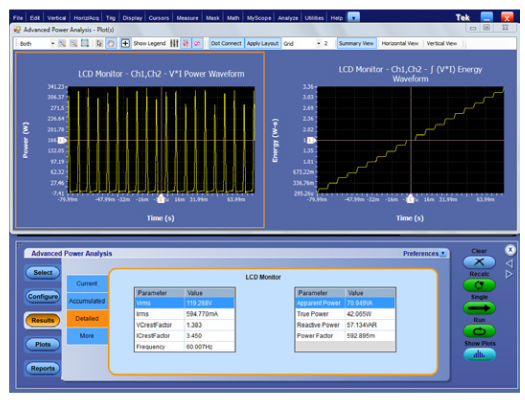
Figure 10 shows the same measurements on the same computer monitor while it is in standby power mode. After turning off the power switch, the power application was simply run again with a push of the application’s Single button. Notice that the monitor is now drawing less than ¾ of a Watt, well below the 1 W design goal. As the power dissipation decreases, the pulses of current become narrower, resulting in a higher current crest factor, and a significantly worse power factor.
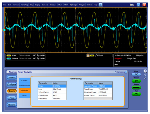
The second example shows power quality measurements, made with the same test setup, at the line input of a 1.5 Amp laptop PC power adapter. While the computer is running and the battery is still charging, the adapter draws about 24 Watts. After the computer battery is fully charged, the power draw drops to about 21 Watts, as shown in Figure 11. Again, notice that the current is drawn in pulses, resulting in a high current crest factor and low power factor.
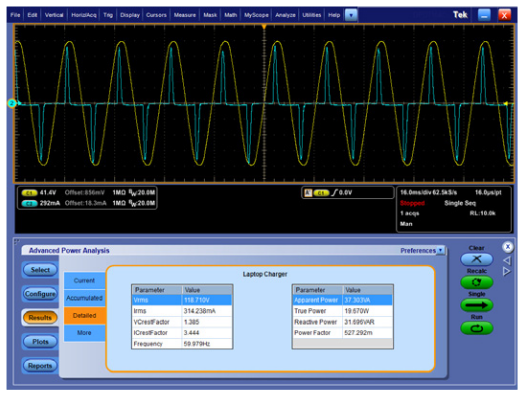
Figure 12 shows that the power drops to less than 1 Watt when the laptop is turned off and the power application’s Single button is pressed again. Notice that the peaks of the current are very small and that there is a significant phase shift between the yellow voltage and the sinusoidal component of the cyan current, indicating a highly reactive load, dominated by the line-to-line capacitor in the input filter circuit. This reactive load is confirmed by comparing the relative magnitudes of the True Power and Apparent Power measurements.
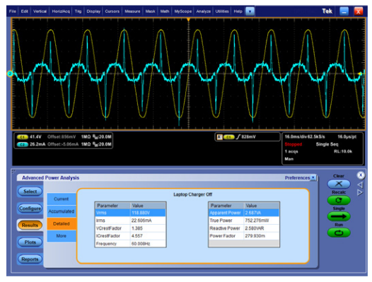
When the laptop is disconnected from the power adapter, the power drops even lower, as shown in Figure 13, though the general characteristics of the waveforms are similar.
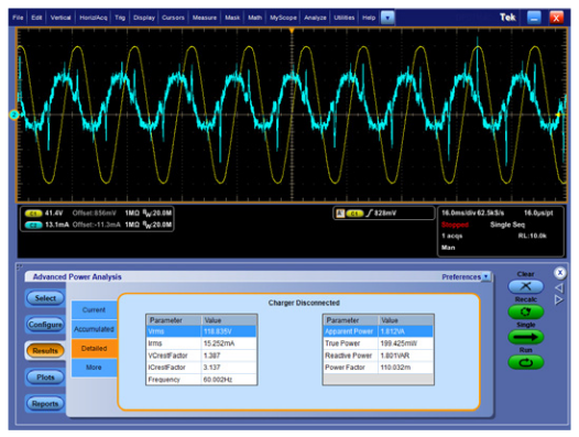
The third example, made with the same test setup, shows power quality measurements made on a 0.15A cell phone charger. While the phone is charging, the adapter draws just over 2 Watts of power, as shown in Figure 14.
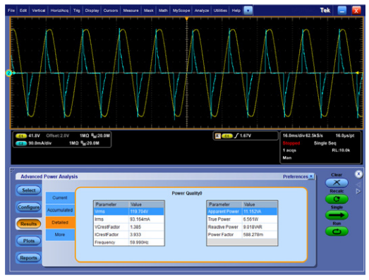
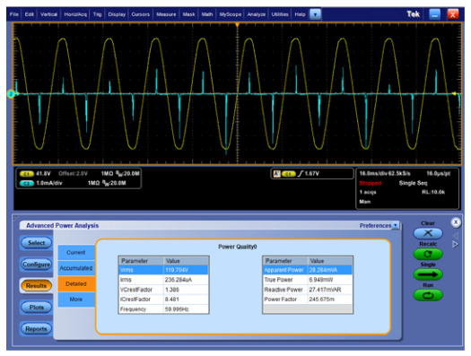
When the cell phone battery is charged, the power drawn by the adapter drops to about 85 milliWatts, as shown in Figure 15, well below the 100 mW design goal.
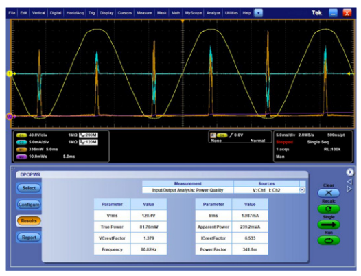
The final example shows power quality measurements made at the line input of a battery charger for a Bluetooth hearing aid pairing device after the device is fully charged. Figure 16 shows the DPOPWR automatic power quality measurements. In this case, notice that the current is only drawn in very short pulses, as indicated by the high current crest factor measurement. The instantaneous power is also pulsed but has a low average value for the power loss. Again, the standby power is well below the 100 mW design goal.
Conclusion
Using the measurement techniques described in this technical brief, low-power measurements such as standby power can be easily and accurately made using an oscilloscope and highperformance power probes. When automated by a power measurement application, these measurements can be made easily and repeatably.
Find more valuable resources at TEK.COM
Copyright © Tektronix. All rights reserved. Tektronix products are covered by U.S. and foreign patents, issued and pending. Information in this publication supersedes that in all previously published material. Specification and price change privileges reserved. TEKTRONIX and TEK are registered trademarks of Tektronix, Inc. All other trade names referenced are the service marks, trademarks or registered trademarks of their respective companies.
11/13 48W-28259-1

