
Abstract
Many high-speed serial interface standards call for a test known as 'Stressed Eye.' This paper is an introduction to stressed eye testing, some of the high-speed standards that use it, and how a receiver test using stressed eye is constructed.
Jitter Tolerance Testing of Receivers - The Basics
The Job of the Receiver
The formal name of stressed eye testing is ‘receiver jitter tolerance test’ the ability of a high speed electrical or optical receiver to deal with an impaired incoming signal (with jitter and crosstalk on it) and not make a mistake. In other words, how bad can the incoming signal be and not cause the receiver to misjudge a one to be a zero, or vice-versa, creating errors.
Conceptually most digital communication links are the same, whether they are trans-oceanic fiber optic links or high-speed connections across a circuit board or backplane. A transmitter puts out a good clean signal; the signal passes through a hostile environment that corrupts it in various ways, and the receiver’s task is then to reconstitute the original stream of ones and zeros without making a mistake.
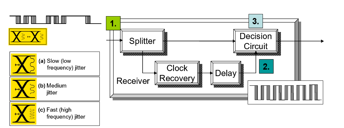
At speeds above 1 Gb/s, it is very common that the data signal being transmitted has a clock signal encoded within it. In order for the receiver to correctly interpret the incoming data, it needs a timing reference that is related to the data. As the hostile environment that the data signal passes through can alter the timing of the signal in unexpected ways, deriving the timing signal from the incoming data makes sense. An oversimplified block diagram of a receiver is shown in Figure 2. While it omits amplifiers and other components, it is useful to get some relevant ideas across.
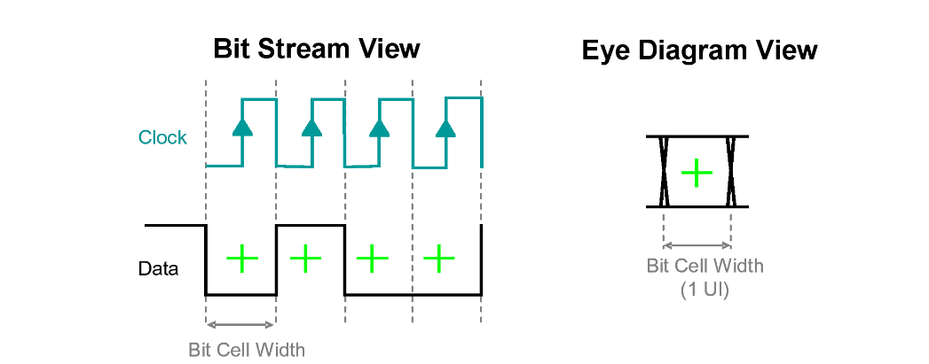
The clock recovery circuit derives a data-related clock signal from the data. The aim is to use this clock to time the execution of decisions on the incoming data - for each bit time slot, whether the signal should be a one or a zero. The decision circuit will look at an instant in time, and at that instant decide whether the data is above or below a threshold point. From this, the circuit will produce a new, clean one or zero, respectively. This is shown in Figure 3. The clock recovery circuit of Figure 2 produces a clock signal, and the delay is then used to position the rising edges of the clock signal in the correct position within the eye to time the decision (where a green cross shows the time instant where a threshold decision is taken).
Also shown in Figure 3 is the picture in eye diagram form — where the bit sequences of the incoming data, such as 0-0-0, 0-0-1, 0-1-0, 0-1-1, etc., are overlaid on a single bit cell to show a combined picture of the system’s signal integrity (right side of the figure).
The process described above assumes idealized data coming in. Obviously the real world is not like this, and the signal that reaches a typical receiver is usually of smaller amplitude than needed, contains noise, and has other impairments. We will look at some of these in more detail later. So what is jitter tolerance?

The Effect of Jitter
Jitter is often explained as the non-ideal placement of data edges with respect to a clock. Jitter is a complex subject, with many pages written about it elsewhere — we’ll keep it simple for this discussion. Figure 4 shows the data signal of Figure 3 undergoing jitter — some edges in the data stream have moved from their ideal position. If this were to happen, it is easy to see that some of those edges might start to interfere with the decision making process, with mistakes increasing the more the edges move across the bit cell.
A major advantage of using encoded clock and then recovering it from the data is that the clock recovery can be used to produce a clock that tracks, or moves with, the data signal even as it moves around in time. It is intuitive that if there is an overall trend for all edges to slowly move around together in time, that the clock recovery delivering a related clock signal could track this slow movement. It is also intuitive that if the movement of edges were very fast or completely erratic bitto-bit, that a clock recovery circuit would have trouble tracking this. This leads to the idea that a clock recovery circuit can act as a jitter filter, with the ability to track slow-moving jitter up to some limit, resulting in a data stream that has reduced jitter related to the recovered clock. Let’s look at how this works.
How Clock Recovery Can Help
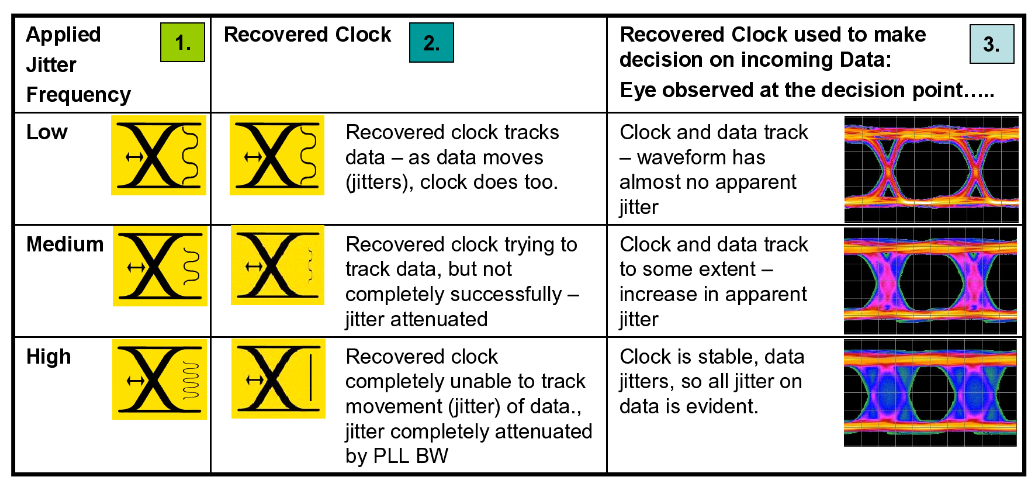
Using the receiver of Figure 2, we will apply a modulation to the edges of the data signal. This will have the effect of moving the edges in one direction, for example making them late an increasing amount, then bringing them back in line again, and then making them early for a time. This will happen over and over again, in a manner that is related to the modulation signal generator we choose for this experiment (rather than in any way related to the pattern of ones and zeroes of the data stream). For this example, we’re going to use a sine wave of different frequencies.
Figure 6 shows the receiver under three different conditions of applied sinusoidal jitter. The first column of the table examines the jittered signal appearing at the input to the receiver (1). The second shows what the clock recovery circuit (often a Phased Locked Loop, or PLL) produces (2). The third column shows the signal appearing at the receiver decision point. This may not be intuitive. For the slowly varying edges, the clock that is recovered is an exact mirror of the data, with the edges moving at the same rate and by the same amount as the data edges. The net effect is that, each instant a decision is made, the decision circuit sees a bit cell perfectly synchronized with the clock strobe, and the decision is made correctly every time. At high frequencies, beyond the ability of the PLL to cope, it attenuates the jitter present on the recovered clock. The data edges come in heavily jittered, but the clock does not move in sympathy with the data at the decision circuit, and so the net effect seen by the decision circuit is edges that are moving in time with respect to the clocking signal. This obviously increases the chance of errors.
Note that the amount of jitter on the incoming data did not change – only the frequency of the jitter did.
Testing a Clock Recovery Circuit with Sinusoidal Jitter
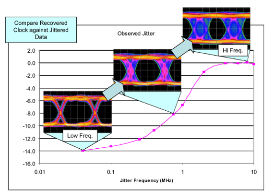
At 10 Gb/s, typical clock recovery circuits switch over from tracking the jitter out, to fully passing the jitter on, with a transition in the region of 1 – 4 MHz. The graph in Figure 7 shows the transfer function of one such clock recovery unit.
Sinusoidal Jitter Templates
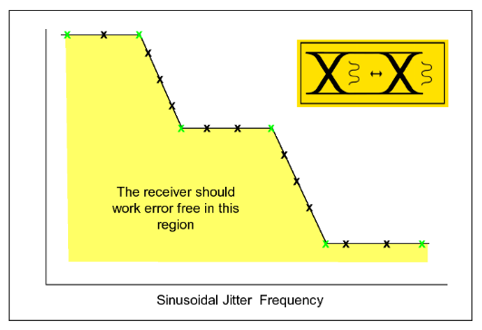
We’ve seen that the clock recovery circuit in a receiver can have a big effect on the effectiveness of the receiver in dealing with jitter. Receivers are usually tested for jitter tolerance by applying a jitter modulation of different frequencies and amplitudes to the incoming data signal, and counting when errors occur. Jitter tolerance testing thus requires a BERT error detector and some kind of impaired pattern source. The testing often uses a sinusoidal modulation of the data signal transitions, with instructions on how much modulation should be applied in the form of a jitter template graph. An example is shown in Figure 8. At low jitter frequencies, a receiver is often expected to endure large amounts of jitter — many unit intervals (UI), enough to close the eye completely many times over. At these low frequencies though, the clock recovery is expected to completely remove the effect of the jitter. At higher frequencies, the amount of jitter applied is less than 1 UI.
When testing, a number of discrete points is chosen on the template, usually a compromise between confidence that the device will comply, and minimizing the test time. Usually more attention is paid to the areas where the template gradient changes (the green crosses in Figure 8).
The SONET/SDH Way
The jitter tolerance method described above, using sinusoidal jitter stepped through a template, was pioneered by the SONET/SDH world. The original implementations of such networks were to have a transmit end of the link and a receive end, and repeaters in between. Each repeater converted the optical signal back to the electrical domain, cleaned it up and amplified it enough to drive the conversion back to the optical domain and the distance to the next repeater (this type of regeneration is less common following the invention of fiber amplifiers that reduced the need for the conversions between optical and electrical domains along the way). In such ‘repeatered’ systems, signal-to-noise was the biggest impairment to system performance, but it was essential that repeaters didn’t have the effect of amplifying jitter along the way, which is very possible in such systems.
Jitter Tolerance in More Recent Standards
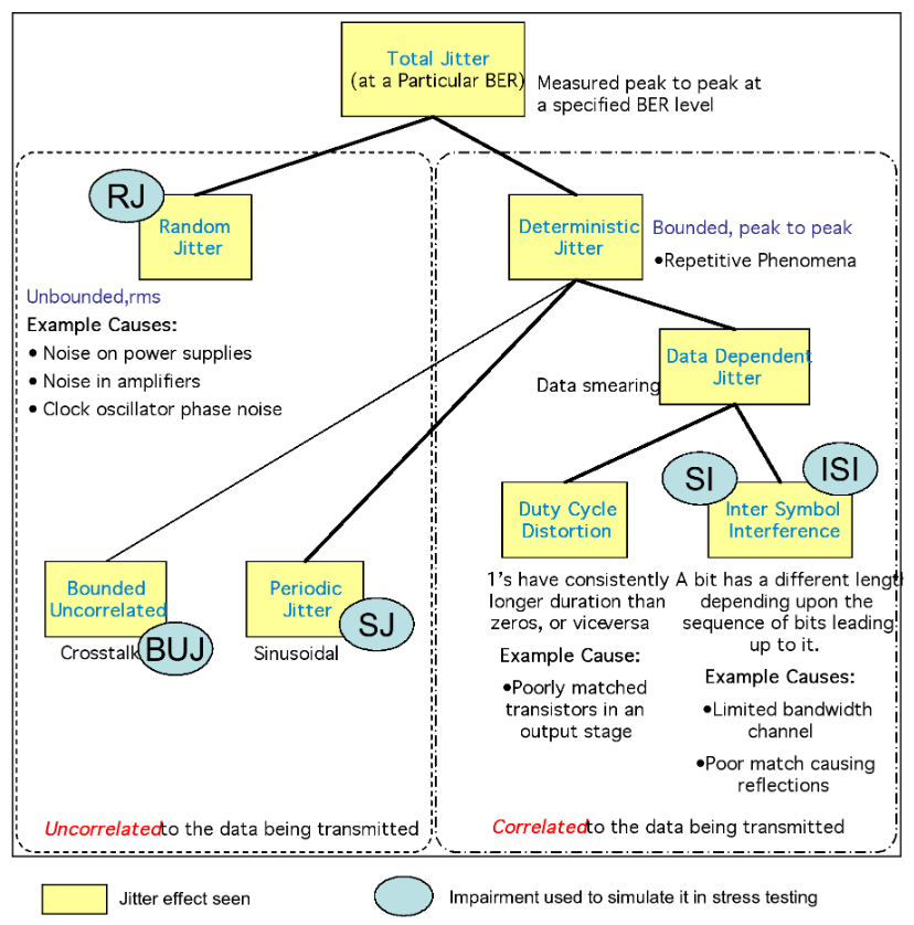
While it made sense in a repeatered SONET/ SDH environment to measure jitter tolerance with a sinusoidal jitter template, many of the more recent standards have been tackling communications links of a very different sort. One thing that they have in common is that such systems, whether optical, electrical cabling, or across backplanes and circuit boards, is that signal-to-noise is often not the limiting factor in performance. This has led to the creation of more complex recipes for the impairments that are introduced to a receiver being tested. Stressed eye testing usually imposes restriction around the entire eye, not just the time axis, and so is not just a jitter test anymore. As discussed later, a combination of some or all of the following impairments are used to create the stressed signal.
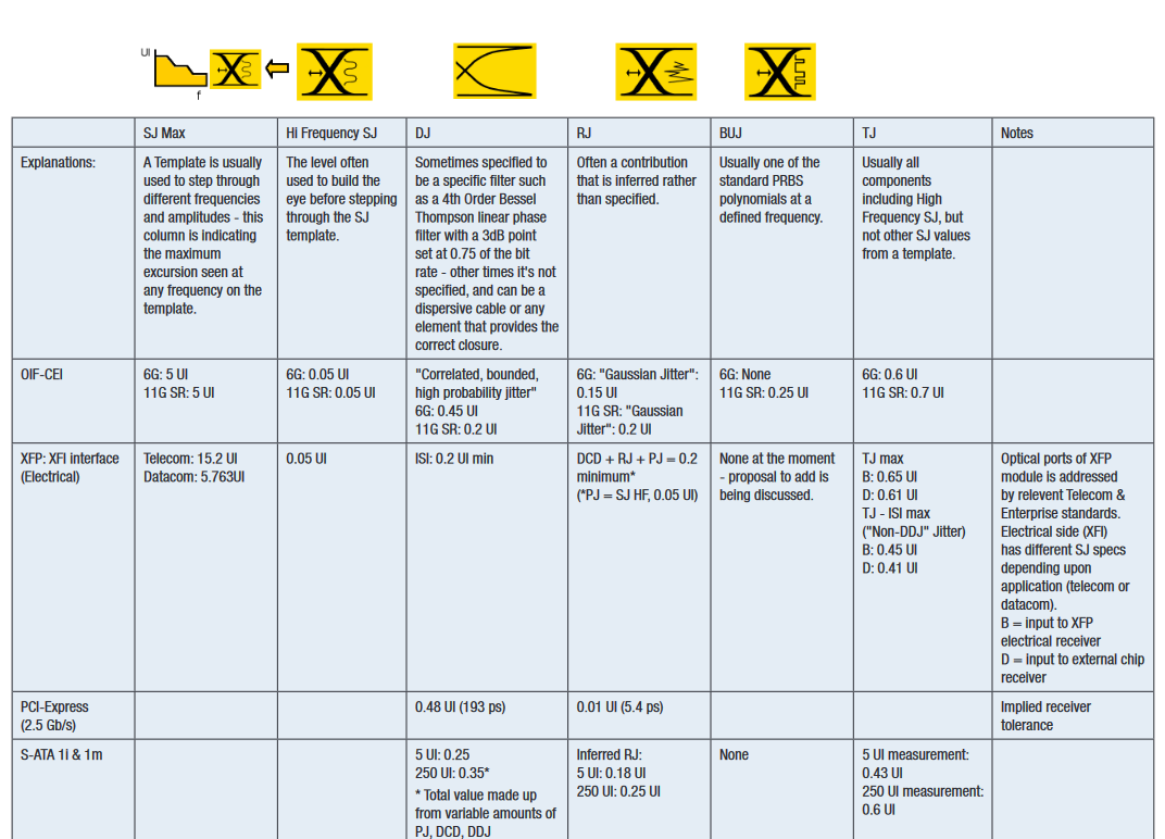
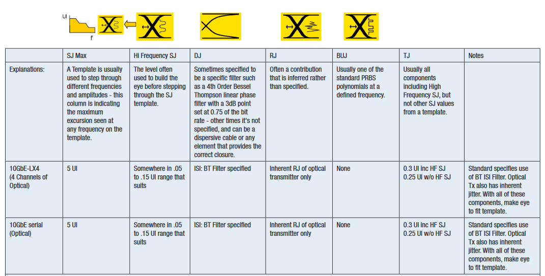
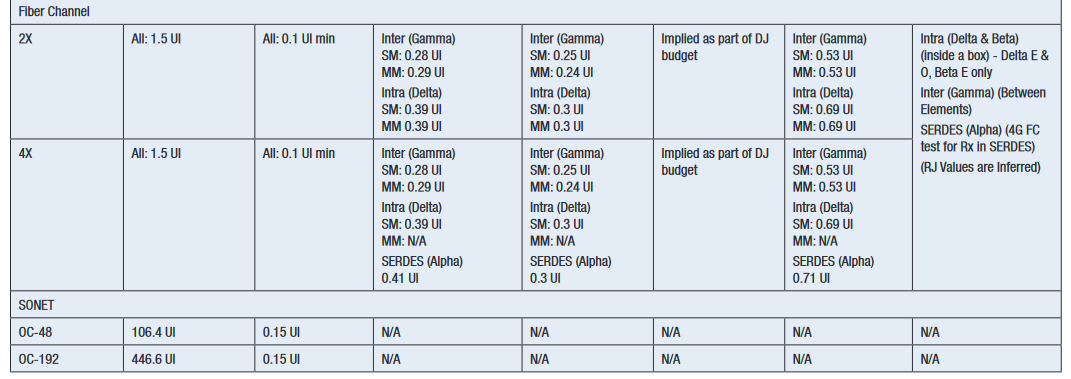
The first standards to use stressed eye were Gigabit Ethernet and 1x, 2x and 4x Fiber Channel between 1998 and 2003. During this period, stressed eye was adopted and modified by the emerging 10 Gigabit Ethernet standard (2002). Since then, different recipes of stressed eye have been adopted in many standards, including high speed buses such as PCI Express and Serial ATA. A table of recipes for common standards is given in Appendix 1. A common theme for many standards is the amount of inferring and guesswork required to interpret what is necessary
Impairment Types
A Brief Note on BER Contour
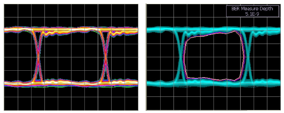
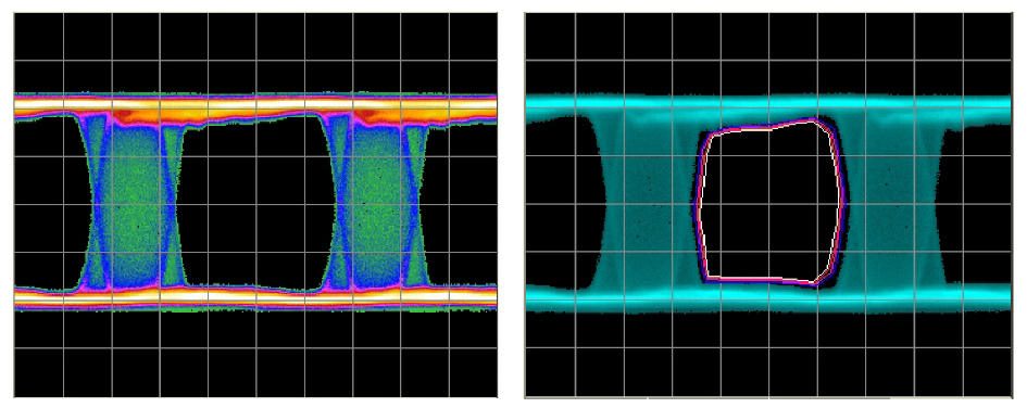
The new stressed eye recipes are intended to reflect the likely impairments that a receiver may be faced with. In the following list, the impairments are illustrated with real eye diagrams and BER contours. More detail of BER contours is obtainable from SyntheSys Researchi, but briefly the contours are like the contours on a geographic map, showing the steepness of mountains. In an eye diagram, the steeper the slopes, the less likely edges are going to intrude on the decision point and cause errors. An advantage of BER contour is that it goes much deeper than conventional oscilloscope eye diagrams in revealing the infrequent events, such as random jitter, that must be controlled for error-free operation to be achieved. In the following examples the outermost (blue) contour shows where the 1x10⁻⁶ boundary is — that is, if the receiver decision point were to be moved to somewhere along that line, the receiver would achieve a BER of 1x10⁻⁶. The innermost (white) contour is, usually, a projected line showing where 1x10-16 operation would lie. Placing a receiver decision point inside this boundary is assumed to allow error-free operation. Obviously the more area that lies within the inner boundary, the healthier the eye is considered to be.
A Clean Eye

Sinusoidal Jitter

It is obvious from the eye diagram that the eye undergoes closure in the time axis, which is the aim in simulating jitter. It is useful to note that the BER contour shows very tightly grouped contours. This means that all of the closure is obvious in the eye, with no infrequent events lurking to catch out the unwary. The jitter modulation is entirely deterministic,completely bounded.

Sinusoidal Interference

The result is similar to using sinusoidal modulation to close down the time domain. The eye looks closed in the amplitude axis, but the BER contour shows the impairment to be entirely well-behaved, leaving plenty of area of operation clear for the receiver decision point.

Random Jitter

Most often this can be from low cost PLL-synthesizer parts used as clock sources.
Broadband RJ is not much of an issue in copper links, but strong in optical links through use of a post-amplifier after the receiver.
Also in optical links, at the optical receiver input there can be a blend of low frequency jitter mixed with high frequency laser and laser/fiber noise. The high frequency transmitter jitter may be filtered in long cable plants.
850-nm links based on VCSELs commonly exhibit significant levels of RJ.
Amplifier noise adds noise to data edges, with the consequence that the slower an edge, the more conversion there is from amplitude to time domain.
Looking at the eye diagram of Figure 12, the eye looks fairly open, with little to worry about. The reality the receiver will experience is shown in the BER contour. This is the first example here of an impairment that has rarely occurring events. This is known as an unbounded process — it is not deterministic, in that imposing the same conditions such as a particular pattern sequence does not necessarily yield the same result in BER terms. In this case, there is a finite probability of an edge appearing in any position across the eye and causing errors. Largely spaced contours such as those shown in Figure 12 are a warning sign. For this reason, if RJ is called for in a recipe, it is important to set it up carefully, preferably using a BER contour or deep jitter measurement to be sure the amount is correct.
Typical test setups will have some inherent RJ anyway (they are composed of active components). Some standards specify adding no more RJ than is already present, others require extra, and this usually means adding amounts until the combination of inherent and added RJ reaches the correct level.
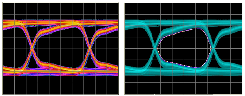


ISI

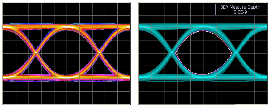
In each case, the effects are entirely deterministic — that is, using the same data patterns in the same way will produce the same eye closure every time. A few things to note:
Figure 13 uses a special kind of filter known as phase linear, producing the symmetrical waveform shape shown. Figure 14, using a poor-quality piece of coax, is asymmetric and shows a capacitive effect. In both cases, the pattern used is a 27 –1 PRBS — a very short pattern at 127 bits long, and one that doesn’t contain particularly aggressive bit sequences. Every single pattern effect is captured in the eye diagrams, with no deterministic rare events lurking, which is why the BER contours of both of these examples are tightly grouped.
Figure 15 is different. The general shape is a variation on a similar theme to Figures 13 and 14, produced here by a backplane. However, a difference becomes immediately clear in the BER contour. The reason for this is that the pattern used was a 231–1 PRBS, a much longer pattern than was used in the other two examples. This pattern has much harder pattern sequences, many of which only occur once per pattern repetition. For a pattern that is over 2x109 bits long, this means that sequences that cause edges to move the most in time will not be seen with a conventional sampling oscilloscope. This is important, as many standards require use of long patterns (such as 223–1 and 231–1 PRBS) to do stressed eye testing. Note that the BER contours in Figure 15 look like they might be caused by some random process such as the RJ case of Figure 12. This isn’t quite true — patternrelated effects are bounded. As long as you are able to see all effects in the measurement you are making (such as a BER contour run for long enough) then you will capture the latest edge that will occur. Using a shallower view, infrequent event pattern effects can appear like RJ.
BUJ

The measurement in Figure 16 was made using a 27 –1 PRBS modulation of the data edges. Because the patterns used are all short and the effect bounded, you would expect to capture the full edge excursions in a typical eye diagram.
Adding the Components Together
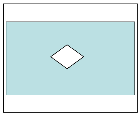
Typically a stressed eye recipe will have two parts — a sinusoidal jitter template such as the one we saw in Figure 8, used to step through the different sinusoidal modulation frequencies and amplitudes, and an eye mask such as is shown in Figure 17. The idea is that the different components specified are added in to close the eye down (blue area) to the diamond, leaving an assured area of error-free operation in the center (white area within the diamond). The receiver is expected to operate successfully in this small area, despite the impairments.
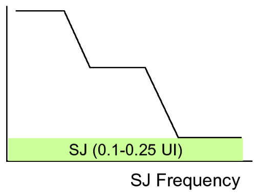
Setting up components to the template can be achieved in a couple of different ways, depending on the standard. Standards such as XFP require the recipe to construct the eye to the template without SJ being part of it. Once the template is complied with, the SJ template is stepped through. The other approach, as used by standards such as 10 GbE and XAUI, is to construct the stressed eye to the template including SJ, set to the value it has at its highest frequency (see green segment of Figure 18), typically somewhere between 0.1 and 0.25 UI. The other components are then added in to match the mask template, and then the SJ template is stepped through.

In both cases, the aim at the end is to have introduced the stressed eye stimulus to the receiver, step through the SJ template and to count errors. Often engineers will use the template as a basis, but for a given frequency on the template, will step up in amplitude until they hit the limit of performance to assess device margin (or step downwards to explore where a device failed compliance). See Figure 19. Similarly, margin can be added in the eye template by making the diamond smaller.
Conclusion
We’ve walked through the history and makeup of jitter tolerance testing using a stressed eye. We’ve seen that stressed eye testing has evolved, appearing in many diverse high speed standards for receiver testing, often exercising the receiver in time for more than just a sinusoidal stimulus, and also the amplitude dimension. Some of the common reasons why standards choose particular stress components have also been explored, along with the construction of a typical stressed eye to a template.
