
Semiconductors are used in many more places than computers and tablets. They are found in everything from electronic medical devices to the latest electric vehicle and handle a diverse array of tasks. Most people just assume all this is accomplished with “silicon” enabled by Moore’s law and faster processors.
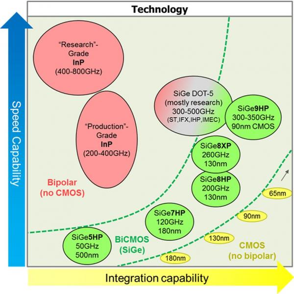
However, as detailed in a guest blog post by Tektronix CTO Kevin Ilcisin published in Electronic Design, traditional CMOS is just one of many different semiconductor manufacturing processes used in modern electronics. In fact, compounds such as silicon germanium (SiGe), gallium arsenide (GaAs), indium phosphide (InP), gallium nitride (GaN), and silicon carbide (SiC) offer advantages such as fast switching times or higher performance that make them better suited to a particular application than CMOS.

In his post, Ilcisin first walks through these various processes and then provides tips and high-level suggestions for how to evaluate the different processes for particular applications. As an example, he also looks at the different technologies commonly used in test and measurement instruments. Even though CMOS continues to improve, oscilloscope performance requirements far exceed the capabilities of CMOS alone leading to adoption of processes like SiGe in the case of Tektronix oscilloscopes.
For the full post, head on over to Electronic Design.


