Introduction
It's late at night and you're driving home. You're tired and just want to get to bed. But then, suddenly, you are faced with a big animal in the middle of the road. Immediately, your car slams on the brakes to prevent you from hitting the animal and from swerving off the road. Through the technology of light detection and ranging – better known as LIDAR, your vehicle or the autonomous vehicle has protected you from danger.

LIDAR is a 3D sensing method that uses pulsed laser light at various wavelengths to measure variable distances to detect objects in front, behind, or on the sides of the vehicle. At the heart of the LIDAR system is the vertical cavity surface emitting laser (VCSEL), a semiconducting device that emits laser light vertically from its top surface. A VCSEL discharges the light perpendicularly from the surface, which makes it the perfect device for a LIDAR system.
One advantage of the VCSEL is its manufacturability on a semiconductor wafer, making it easy to test its electrical and optical performance. And, given that a LIDAR system requires thousands of individual VCSELs in arrays to perform its mission-critical application, significant testing must be performed at various stages of the production workflow. By testing at various phases, you eliminate bad VCSELs early on to prevent unnecessary processing of bad parts, which keeps overall fabrications costs down.
As the demand for distance and velocity measurements in 3D space grows, VCSELs used in LIDAR systems may be driven with electrical pulses having pulse widths of a couple of nano seconds with rise times less than 1 nanosecond. But in the case of early wafer level or package level test, tens of microsecond pulses have been applicable because of the difficulty to drive nanosecond pulse widths from a test system over a couple meters of cable to the device under test. At early stages of production test, current as high as 10 A is required to test VCSEL arrays for some applications. The challenge that the industry is facing is generating short pulse widths with microsecond rise time at the current levels required. Why is this so important?
The introduction of higher test currents into a VCSEL on wafer, or even a packaged part increases device self-heating, which can degrade the performance characteristics of the device, or worse, damage it. It also increases the potential for burning probe tips during on-wafer testing. This can be problematic, seriously compromising yield. To minimize self-heating, many test specifications require current pulses with pulse widths as short as 10 µs. This requirement in turn drives the need for pulse rise and fall times on the order of 2 µs or less in order to make a fully settled measurement on such a short pulse. While conventional instruments like source measure units (SMUs) are commonly used to test VCSELs, they may not be able to achieve the short current pulse widths needed and will even require manual tuning to ensure the pulse output is usable.
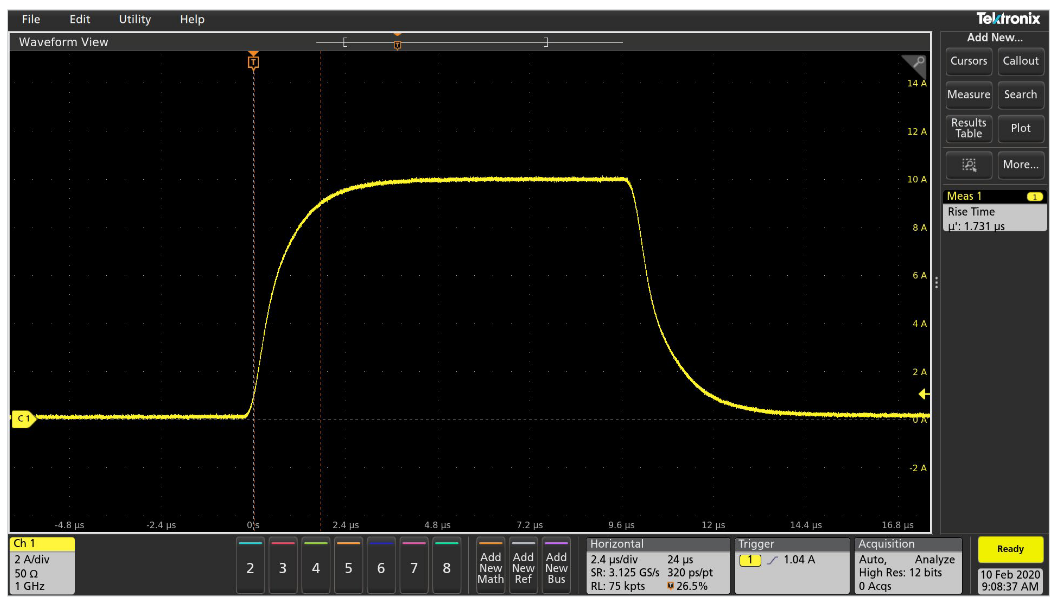
The need for tuning by some current sources (SMU or otherwise) highlights one of the key issues when outputting short 10 µs current pulses – test circuit inductance and impedance due to the device-under-test (DUT) and any cabling or switching used to route the pulses to the DUT. For most SMUs, the test lead inductance will affect the instruments' ability to source a clean pulse with fast rise time, no overshoot, and no undershoot. Outputting very clean pulse waveforms as shown in Figure 2 is critical since more than 90% of VCSEL customers require the pulse current waveform to be stable to ensure accuracy of optical peak power, near field, and far field measurements.
Why is Cable Inductance a Challenge?
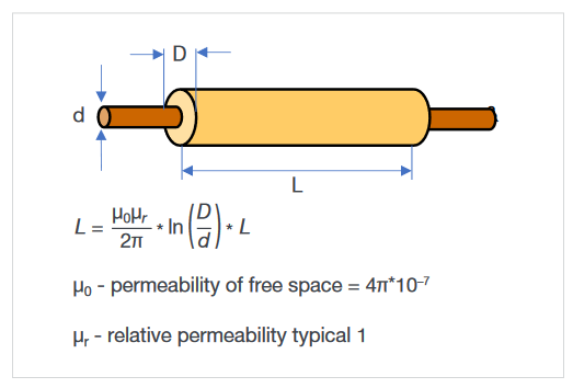
Coax cable is widely used to transmit fast signals to a device under test. Each cable has its own characteristic cable impedance which is a relationship of the capacitance and the inductance. The most critical factor between the two is the cable inductance in order to deliver a clean 10 µs pulse. The variables needed in calculating this inductance are center conductor diameter, distance to outer shield, and length shown inFigure3. The relative permeability of coax cables, which depends on the material of the insulator, is usually 1. For example, the calculated inductance of a coaxial cable with 1 mm inner diameter, 3.5 mm outer diameter, 1 m length, and relative permeability of 1 is applied, is 250 nH which is a somewhat typical value for coaxial cable inductance. Unshielded cable can have much higher inductance.
In most cases, two coaxial cables are used in parallel from the test instrument to the DUT connected to the high terminal and the other to the low terminal. The problem is that the inductance of the two cables is not double the inductance of just a single cable. It could be as much as 3 to 6 times higher depending on how the cables are routed from the instrument to the DUT. For example, a 1 meter cable with 250 nH inductance is not 500 nH in two paralleled cables but can be as high as 1.5 µH. Extra loop inductance can be created depending on how far apart the cables are. To eliminate the loop inductance, the shields of the two cables should be tied together at both ends of the cable.
The most significant challenge of high inductance in cables is overcoming oscillations, overshoots, and undershoots in the current pulse. Where capacitance can result in oscillation in a voltage pulse, inductance will have a negative impact on output current stability. For example,Figure4 illustrates the impact of several inductive loads on a 100 µs pulse.
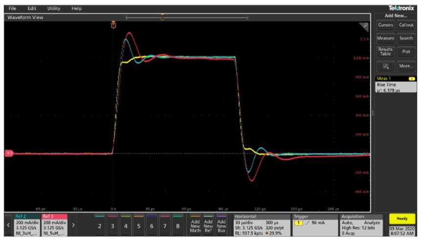
The results of the test show that increasing inductance increases the level of overshoot and instability of pulse shape. The instability can make it hard to make accurate measurements because the pulse settling time may be too long.
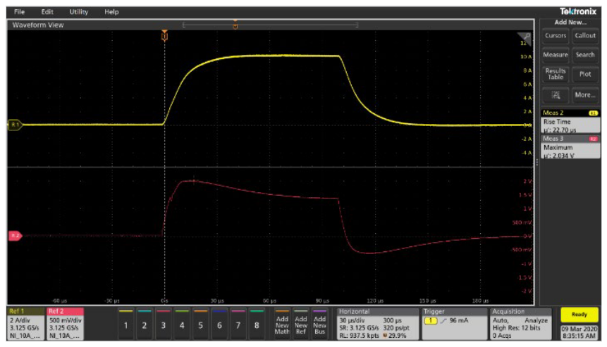
Another issue with respect to the inductance of the cable is the amount of voltage that develops at the rising and falling edges of the pulse. The instantaneous voltage across an inductor is given by L×di/dt, where L is the inductance and di/dt is the rate of change of the current with respect to time. As you might guess, the shorter the rise and fall times, the larger the voltage that develops at the edges. In Figures 5 and 6, a 22 µs rise time in the pulse results in a 2 V voltage at the rising edge, but a 1.6 µs rise time creates about a 10 V voltage spike. This voltage spike can give the instrument some burden in voltage at the edge. The instrument must support the voltage peak. If it is limited in voltage, it could be slow at the rising edge. The more serious problem of the high voltage peak in fast pulsing is the requirement of an additional settling time to make precise voltage measurements.
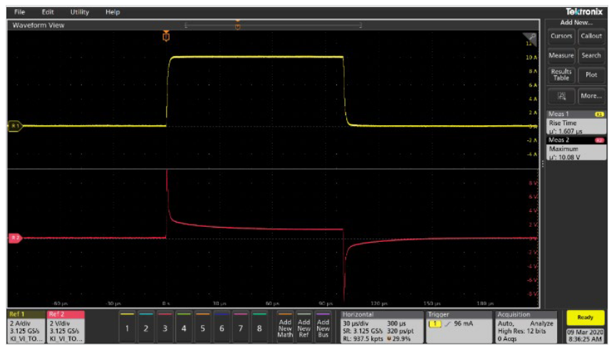
The challenge comes down to how to provide a usable current pulse to the device that results in no oscillations, overshoot,and undershoot so you can properly test the device and make accurate voltage measurements even with varying cable inductances and device to device inductance variability.
Manual tuning to improve pulse fidelity
Even though the inductance of cables can be reduced as low as possible, there will always be some level of inductance in the cable and in the DUT. When testing devices like VCSELs on a wafer, there will always be variability in the inductance from device to device. All together this can result in different shapes of the fast pulse, making it difficult to have a clean high fidelity,repeatable pulse shape to test every device.
To overcome these challenges, some SMU suppliers provide the means to manually tune the pulse output to compensate for test circuit inductances. Manual tuning is used to adjust the pulse output shape to minimize oscillation, overshoot, undershoot, and optimize the rise time so the pulse is more usable. Depending on the instrument supplier, you may have to tune various parameters or combinations of parameters such as bandwidth, compensation frequency, zero pole, load impedance, and rise time. Improving the bandwidth helps to create a short pulse but is limited by the closed loop gains, which is dependent on the load impedance. Unfortunately, this is not sufficient to eliminate overshoot or oscillation completely at the pulse rising edge. Another factor that is adjusted to minimize overshoot and oscillation is to control the rise time. But eliminating overshoot and oscillation results in a longer rise time. Longer rise times may not be acceptable in many tests. And, even if the pulse output is tuned to a particular current level, there is no guarantee that the manual tuning will result in consistent pulse waveforms, especially when you are testing a VCSEL with a pulsed IV amplitude sweep in R&D and production.
To demonstrate this, we looked at two competitive SMUs that offer manual tuning to see what the output pulses look like under different conditions.
Test 1: 10 A @ 100 µs into 0 µH, 1 µH, 3 µH, 5 µH loads


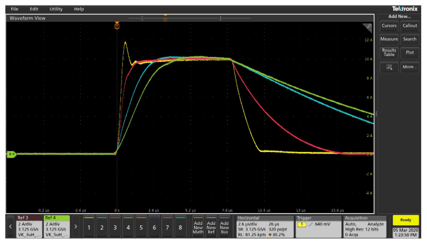
The results of this test would drive the following conclusions:
- Without tuning, overshoots/undershoots increase with increasing inductance levels.
- When tuned, the inductance impacts the rise time, mostly slowing it down. It can also impact the fall time, sometimes lengthening it.
Test 2: 1A @ 100 µs into 1 Ω, 2.5 Ω, 5 Ω, 7.5 Ω, 10 Ω loads. Tuned at 1 A and 1 Ω.
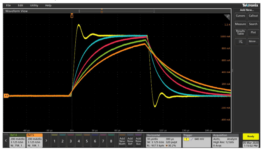

Given that the system was tuned at 1 A for 1 ohm for a 100 µs pulse width, the results of this test would drive the following conclusions:
- Tuning at one resistance level does not guarantee similar pulse shape results at other resistance values.Waveforms are inconsistent.
- High resistances can result in longer rise times and longer fall times.
Since most engineers will be testing VCSELs that require a light-current-voltage (LIV) test, sweeping the pulse current is part of the essential testing to ensure its reliability for post-production use. The test helps to verify the operating characteristics of VCSEL or other laser diodes. To gain some insight into this, we ran an amplitude test on the competitive SMUs to determine how they would perform when testing a real VCSEL.
Test 3a: 100 µs @ 1 A, 2.5 A, 5 A, 7.5 A, 10 A. Tuned at the 1 A level.

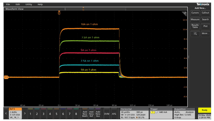
Given that the system was tuned at 1 A for a 100 µs pulse width, the results of this test would drive the following conclusions:
- Tuning at one amplitude level does not guarantee similar pulse shape results at other amplitudes of current.
- Tuning does not guarantee consistent pulse widths at different amplitudes
Most VCSEL customers are demanding shorter pulse widths, as low as 10 µs. Since Competitor SMU A was not capable of outputting a 10 µs pulse width, we only looked at Competitor SMU B.
Test 3b: 10 µs @ 1 A, 2.5 A, 5 A, 7.5 A, 10 A. Tuned at the 1 A level.
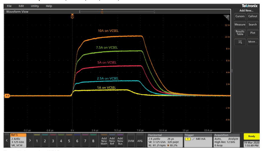
The results of this test would drive the following conclusions:
- Tuning does not guarantee consistent pulse widths at different amplitudes
- Tuning does not guarantee consistent rise times
For production testing where LIV testing is a primary test, one can draw a conclusion that manual tuning is not convenient or efficient on the production floor. This is why the industry has been requesting companies like Tektronix/ Keithley to make faster and higher current sourcing and measuring equipment to deliver the performance they need.
Reacting to the challenges we heard from our customers, Keithley – a Tektronix Company – developed the new 2601B-PULSE System SourceMeter® 10 µs Pulser/SMU Instrument. The new 2601B-PULSE with PulseMeter™ technology is an industry-leading high current/high speed pulser with measure plus the full functionality of a traditional SMU. This new pulser offers leading 10 A current pulse output at 10 V with a pulse width minimum of 10 μs, perfect for testing VCSELs used in LIDAR, LEDs for lighting and displays, semiconductor device characterization, surge protection testing, and much more.
The pulser's built-in dual 1 Megasample/second (MS/s), 18-bit digitizers make it possible to acquire both pulse current and voltage waveforms simultaneously without the need to use a separate instrument. The 2601B-PULSE is a powerful solution that significantly boosts productivity in applications ranging from benchtop characterization through highly automated pulsed I-V and L-I-V production test.
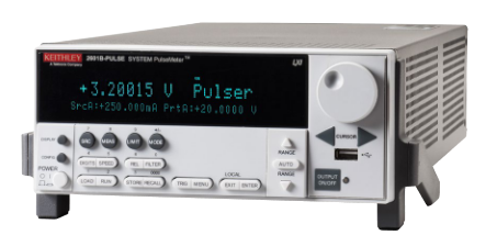
The power of this new instrument is that no manual tuning is required—no matter the current amplitude and into inductive loads up to 3 µH. As previously discussed, some solutions require tuning to compensate for oscillatory behaviors, which can be time consuming. The 2601B-PULSE's control loop system eliminates the need to manually tune for load changes up to 3 μH at any current level up to 10 A so that your pulse has no overshoot and ringing when outputting current pulses from 10 μs up to 500 μs. This ensures a fast rise time, so your devices are sourced with a current pulse to properly characterize the device or circuit. This is very important when sweeping pulse currents through multiple amplitudes, important for a VCSEL pulsed LIV test sweep. To confirm this, we ran the same tests that were performed on the competitive SMUs.
Test 1: 10A @ 100 µs into 0 µH, 1 µH, 3 µH, 5 µH loads

The 2601B-PULSE with no manual tuning required outperforms the competitive SMUs as shown as the four inductance values tested. All rise times were ≤1.7 ms. While the 2601B-PULSE has a maximum load inductance specification up to 3 µH, we were able to run the test at a 5 µH and still obtained similar performance. This may not be the case in all application use cases.
Test 2: 1A @ 100 µs into 1 Ω, 2.5 Ω, 5 Ω, 7.5 Ω, 10 Ω loads.
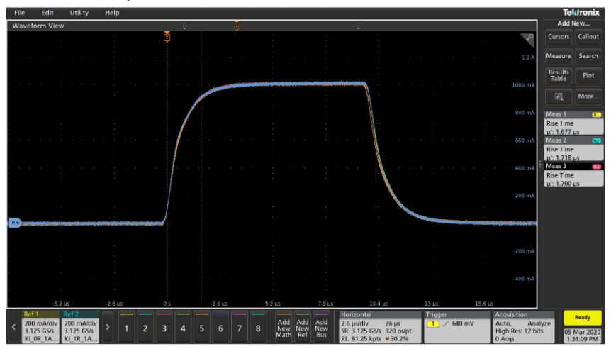
In this test, the 2601B-PULSE with no manual tuning required outperforms the competitive SMUs as shown as the four resistance values tested. The waveforms are identical for all 5 resistances compared to the competitive SMUs. Rise times were also consistent.
Test 3: VCSEL test @ 1 A, 2.5 A, 5 A, 7.5 A, 10 A.

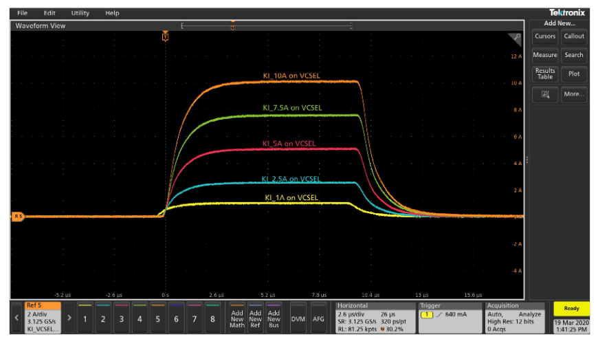
Again, the 2601B-PULSE with no manual tuning required outperforms the competitive SMUs as shown. Pulse widths are consistent and rise times are repeatable for the 5 different amplitude levels.
Conclusion
This white paper has reviewed the impact of cable inductance and how device inductance variability can have an impact on short pulse performance. We have discussed how manual tuning of the pulse output can make some improvements in pulse fidelity but is not necessarily reliable to provide repeatable pulse waveforms, widths, rise times, and fall times. Where cable inductance is kept to a minimum, there are still challenges to generate clean 10 µs, 10 A pulses in various characteristic devices. Our test comparisons show that the 2601B-PULSE offers industry leading current pulse output performance and eliminates manual tuning that is not efficient when testing VCSELs on wafer in high-speed automated probing system. The results clearly show that you can test confidently no matter the current level and with different inductive loads (up to the specification level) to achieve repeatable performance and rise times. The new instrument provides many benefits including:
- No manual tuning of pulse output to ensure high pulse fidelity, reduced testing time, and cost savings in production.
- Make DC/Pulse current and voltage measurements with a single instrument.
- Characterize VCSELs with confidence. Develop the next generation of materials, components, and modules.
- Minimize device self-heating; minimizes burned probe tips. Protect your VCSELs, VSCEL array, LEDs.
- Measure down to single-digit ms sampling rates while outputting 10 µs, 10 Amp current pulses at 10 volts.

