Transitioning from silicon to wide bandgap semiconductors such as silicon carbide and gallium nitride means that power module designs can be physically smaller than what came before, while also increasing MOSFET switching speed and energy efficiency. As competitive pressures make these design parameters more critical, design engineers must reevaluate their approaches to validation and testing
Regulatory and economic pressures continue to push the state of the art in industrial and other high-voltage power electronics toward designs that are smaller, faster, and more efficient. The power-density advantages of smaller and lighter designs are particularly evident in space-constrained and/or mobile usages such as electric vehicles, but compact power electronics are more broadly desirable as well, especially from the standpoint of reduced system cost.
At the same time, efficiency is growing in importance as governments introduce financial incentives and more stringent energy-efficiency regulations. Guidelines issued by global entities, such as the European Union’s Ecodesign Directive, the United States Department of Energy 2016 Efficiency Standards, and China's Quality Certification Centre (CQC) Mark govern energy efficiency requirements for electrical products and equipment.
The need to enact greater energy efficiency in power electronics stretches from the point of power generation to the point of consumption, as illustrated in Figure 1. Power converters operate at multiple stages throughout the generation, transmission, and consumption chain, and because none of those operations is 100% efficient; some power loss occurs at each step. Chiefly due to energy lost as heat, these reductions in overall efficiency multiply throughout the cycle.

Likewise, in addition to increasing efficiency, reducing the size and weight of power-conversion equipment is critical. Smaller, lighter-weight components typically correspond to lower capital expense (CAPEX), which complements the reductions in operating expense (OPEX) associated with greater efficiency. In addition, the efficiency, size, and weight of power equipment are critical design aspects for many applications. In the context of an electric vehicle, for example, all three factors contribute to increasing the range of the vehicle between charges, while lower equipment cost helps in the effort to bring overall vehicle cost to parity with that of conventional vehicles.
A critical challenge facing the power electronics industry as it works both to reduce physical size and to increase energy efficiency is that these design goals typically compete with one another. For example, increasing the switching frequency of converter circuits allows the size of components such as inductors, transformers, and capacitors to be reduced. That helps enable more compact devices at lower production cost. On the other hand, higher switching frequencies also generate additional heat. Accordingly, the power lost through that heat can create product quality and OPEX concerns associated with reduced energy efficiency.
New materials and techniques for design, production, and testing power electronics are making it possible to use higher switching frequencies, without sacrificing power quality or energy efficiency. These advances promise to enable the creation of improved products that are smaller and less expensive.
Advances in test and measurement tools such as arbitrary function generators (AFGs), source measure unit (SMU) instruments, and parametric analyzers are helping powerdesign engineers obtain more robust results more quickly. This updated equipment helps them meet challenges they encounter on a day-to-day basis, such as the following:
- Simplify test setup to reduce measurement errors
- Reduce measurement times to extract switching parameters
- Increase measurement accuracy for the design of highefficiency converters
The Promise of Wide-Bandgap Semiconductor Materials
While silicon (Si) continues to be the preeminent substrate used for power semiconductors, the industry has reached the limits of what is possible using that material. Accordingly, a new generation of wide-bandgap materials such as silicon carbide (SiC) and gallium nitride (GaN) are becoming more prevalent. Electrically, these substances are closer to insulators than silicon and other typical semiconductor materials. Their adoption is an effort to overcome limitations of silicon that stem from it being a narrow bandgap material, which leads to undesirable conductive leakages that become more pronounced with increases in temperature, voltage, or frequency. The logical extreme of such leakage is uncontrolled conductivity, which equates to failed operation as a semiconductor.
Of these two wide-bandgap materials, GaN is suited primarily to low- to mid-range power implementations, under approximately one kilovolt and 100 amps. A notable area of growth for GaN is its use in LED lighting, and usage is growing for additional low-power usages such as electronics power supplies and RF power amplifiers. By contrast, the technologies surrounding SiC are both better developed than GaN and better suited to higherpower implementations such as power transmission, large-scale HVAC equipment, and industrial systems.
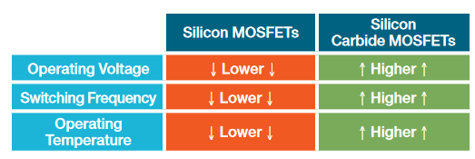
SiC-based metal-oxide-semiconductor field-effect transistors (MOSFETs) offer significant advances over earlier Si devices for use in power modules, as represented in Figure 2. Compared to Si MOSFETs, SiC devices are capable of operating at higher voltages, higher switching frequencies, and higher temperatures. Under these conditions, SiC provides higher performance, efficiency, power density, and reliability. This combination of benefits is helping designers reduce the size, weight, and cost of power converters, making them more competitive especially in lucrative market segments such as aerospace, military, and electric vehicles.

Because SiC MOSFETs enable higher energy efficiency from designs based on smaller components, they are instrumental in the development of next-generation powerconversion equipment. At the same time, this transition also requires engineers to revisit some of the design and testing techniques that they have traditionally used when creating power electronics.
Growing Requirements for More Rigorous Testing
While the types of testing that are required during the design and production of power converters are similar to what was required for previous generations of devices, the adoption of wide-bandgap materials requires added rigor in that testing. Accordingly, more sophisticated test equipment and techniques are needed.
Higher switching frequencies are a key contributor to expanded testing requirements, as wide-bandgap materials enable devices to run in the MHz range rather than the KHz range. For example, operation at higher frequencies requires measurements to be captured at higher speed, and oscilloscopes must accordingly have high enough bandwidth to accommodate these new requirements. Likewise, switching MOSFETs on and off at high frequencies requires an AFG with sufficient bandwidth to provide the needed pulse stimulus.
As mentioned above, an inherent tension exists between switching frequency and energy efficiency. Even as designs operate at higher frequencies in pursuit of smaller devices and lower costs, they must provide higher efficiency. Moreover, regulatory and certification requirements often place added burdens on power equipment providers, in terms of the proof they must supply to verify that their devices meet specific requirements.
Therefore, the drive for energy efficiency is a significant contributor to the need for added rigor in testing; whereas in past decades, the amount of power loss was a low-priority consideration, a power module’s efficiency is today of primary importance. In addition to the efficiency itself being more important than before, data measurements must be robust enough to meet regulatory and certification requirements.
In Search of More Efficient Power-Conversion Designs
In every power-conversion operation, whether it is inversion at a photovoltaic generation site, conversion during longdistance transmission, or inversion to generate an appropriate voltage for end-customer equipment, some power loss occurs. A primary design goal for power converters is to drive down that power loss, bringing the conversion process closer to 100 percent efficiency, as represented in Figure 3.

Here, the change in voltage between the input and output of a switching power converter is accompanied by a corresponding and inversely proportional change in current. Therefore, in an ideal system, the total power at the output of the converter would be the same as the power applied at the input. Of course, that perfect efficiency is a logical maximum that can never be realized in the physical world, with some power always being lost as heat generated by the power converter.
As switching frequency increases, faster operation of the switches in the converter generates additional heat, which corresponds to greater power loss and lower efficiency. While the use of wide-bandgap materials such as SiC mitigates that effect to some extent, the burden falls to power-electronics engineers to take full advantage of the potential benefit.
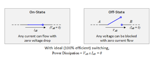
A chief aspect of building efficient power converters is the design of high-quality switching circuits. Ideal switching is instantaneous, and as illustrated in Figure 4, it is also 100 percent efficient, meaning that there is zero power dissipation during operation. The product of the current flow times the change in voltage potential across the switch is zero, in the ideal case; note that in the figure, voltage drop in the switch's on-state is zero, while current flow is zero in the off-state.

While the effort to force power dissipation over a switching structure to zero is asymptotic at best, the attempt is a design imperative. Likewise, the speed of switching in the circuit must be forced toward being instantaneous. To close in on these goals, power engineers must use an increasingly sophisticated set of design and testing criteria that stretches across the entire lifecycle.
Comprehensive Testing Across the Device Lifecycle
Bench testing plays an important role at every stage of the development of power-conversion equipment to characterize, benchmark, and document efficiency and other characteristics. It begins with testing the material to determine whether it is suitable for use, followed by additional testing after the SiC or other wafer has been fabricated but before circuits are lithographed onto it. Testing proceeds on the manufactured MOSFET component, then in an assembled circuit, and finally on the piece of powerconversion equipment when it comes off the assembly line.
Each of these testing phases has individual importance to the undertaking as a whole, and each must be conducted at a specific point during the production process. For example, breakdown voltage testing must be done on a MOSFET as a stand-alone component, before it is installed on a circuit board. Likewise, switching energy must be measured after the MOSFET is installed on a circuit board, because that energy depends on factors associated with the circuit as a whole, with switching frequency depending on the gate driver, for example.
Tektronix and Keithley provide a comprehensive set of test equipment that gives design and test engineers the ability to set up test benches robust enough to meet their most rigorous requirements. This equipment also sets the stage for emerging requirements that will come to the forefront as power-conversion equipment becomes more sophisticated, the regulatory environment becomes more rigorous, and testing protocols become more challenging.
Material-level testing
At the pre-component stage, testing must be conducted on the SiC or other material itself, followed by testing at the wafer stage, to determine the specifications of its behavior. Semiconductor material research and device testing often involve determining the resistivity and Hall mobility of a sample. The main techniques for measuring these parameters are:
- Van der Pauw method
- Van der Pauw method
All of these measurements can be made using a parameter analyzer. The Keithley 4200A-SCS Parameter Analyzer includes modules allowing researchers to perform both van der Pauw resistivity and Hall effect measurements automatically, saving valuable research time and eliminating the need to purchase a separate system to perform these test.
Component-level testing
The next stage of testing occurs for control and simulation during the MOSFET circuit design phase, extending through its post-manufacture as a stand-alone component. Postmanufacture component testing plays an integral role in the MOSFET designer’s creation of data sheets and quality control. It is also used extensively by end customers to validate components against their specifications.
| Test Category | MOSFET | Keithley Equipment |
| ON-state | Vds Vth Vgs-Id Rds(on) |
4200A 2651A SMU |
| OFF-state | Igss Idss BVdss BVdg |
4200A 2657A SMU |
Table 1. Common component-level testing using Keithley equipment.
Also using the 4200A-SCS, we could make these measurements up to 400V differential on the drain. Advantages of using the 4200A-CVIV Multi-Switch include the following:
- No need to reconnect any cables: reduces user error and permits automated testing.
- Allows measuring circuit level capacitance directly.
- Using bias tee at every terminal eliminates the need for external capacitors or shorts.
- Full CV compensation out to the device under test (DUT).
The right combination of test and measurement equipment can provide a powerful solution for power electronics researchers and designers.
Circuit-level testing
As mentioned above, the switching characteristics of a MOSFET must be tested and characterized after installation in a circuit, typically by means of double-pulse testing using an AFG. This testing measures quantities that include turnon and turn-off characteristics as well as thermal behavior. Component manufacturers typically create demonstration boards for internal development use on which they install their MOSFETs for circuit-level testing.
System-level testing
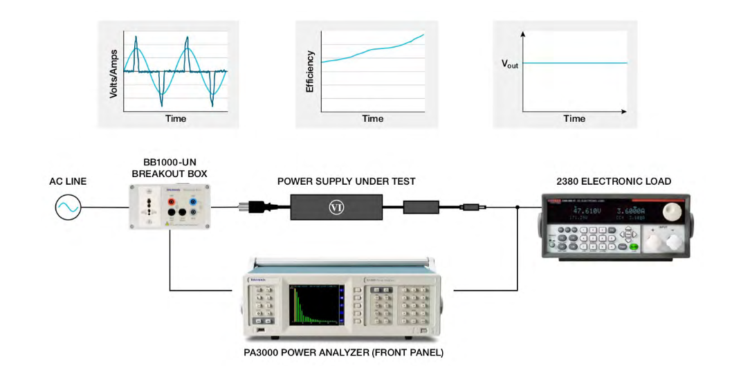
A fully-assembled power module undergoes testing in particular for its operating efficiency using power analyzers, as represented in Figure 5. These measurements play a critical role in meeting regulatory guidelines as well as qualifying for certifications such as Energy Star compliance.

Testing Tools Enable Innovation in Power Electronics
Wide bandgap materials such as SiC are overcoming limitations of their Si predecessors for the development of power MOSFETs. The ability to operate at higher voltages, frequencies, and temperatures than Si set the stage for the next generation of power modules, by delivering a breakthrough combination of cost and energy efficiency. Design and production of semiconductors and power modules based on SiC demand more rigorous testing than with previous generations, and Tektronix and Keithley provide the equipment to conduct that testing quickly and accurately.
Innovations in test tools such as source measure unit instruments, capacitance-voltage units, arbitrary function generators, oscilloscopes, probes, and power analyzers enable design engineers at all phases of the life cycle to work toward power-conversion equipment that can cost-effectively meet rigorous design requirements. Being prepared to certify devices against regulatory changes and the needs of new technologies from power generation to end user devices such as electric vehicles enables companies that make power electronics to focus on the value-added innovation that defines the future.
Find more valuable resources at TEK.COM
Copyright © Tektronix. All rights reserved. Tektronix products are covered by U.S. and foreign patents, issued and pending. Information in this publication supersedes that in all previously published material. Specification and price change privileges reserved. TEKTRONIX and TEK are registered trademarks of Tektronix, Inc. All other trade names referenced are the service marks, trademarks or registered trademarks of their respective companies.
051519 75W-61556-0

