
Abstract
Clock recovery is a common part of many measure-ments, whether as part of the test setup or part of the device under test. We’re going to look at clock recovery from a practical point of view, with emphasis on how it affects measurements. This document closely mirrors the poster "The Anatomy of Clock Recovery, Part 1."
Why is Clock Recovery Used?
Most gigabit communication systems are synchronous; that is, the data within them is timed against a common clock. High speed systems (such as serial buses and optical) usually send NRZ (Non-Return to Zero) data, coded to have the clock it is timed against embedded within it. Whether traveling across inches of circuit board, or across continents on optical fiber, the relationship between data and the clock it is timed against can become disturbed. Extracting clock directly from the data ensures that data regeneration at the receiver can be achieved correctly.
Receivers typically improve the incoming data before passing it on. They do this by passing it through a decision circuit that retimes the data and squares up the pulses. This process is dependent upon a clock signal synchronous with the incoming data, hence the use of clock recovery inside the receiver. Timing variations such as jitter on the incoming data can be reduced or removed if the clock used for retiming moves in the same way at the same time.
As we will see, in practice the operation is more complex than this, and the frequency of the incoming jitter is important.
How Does Clock Recovery Work?
There are many different architectures for clock recovery, and a large amount of literature describing the advantages and disadvantages of each. In measurement equipment, the most common type is based on a phase locked loop (PLL). We will look at this in more detail in a moment. Before we do, it is worth noting that other architectures have been used in measurement equipment in the past.
Older sampling scope clock recovery modules were often feed-forward designs with fixed frequency filters switched in for each rate. Suitable band pass filters are difficult to make with narrow bands. They have also not been frequency agile, and will not track data with moving center frequencies, such as is found in spread spectrum clocking (SSC; see poster "Anatomy of Clock Recovery, Part 2").
PLL-Based Clock Recovery
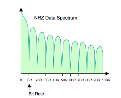
Clock recovery is usually applied to NRZ data. Unlike PLLs used in RF applications, data signals require modification to the PLL design. One challenge is the property of NRZ (NonReturn to Zero) data that there is no discrete spectral line at the data rate. This restricts the types of phase detector that can be employed in the PLL. Examples include Bang-Bang and Hogge designs.
Generic Phased Lock Loop Block Diagram
What it Does
- A Voltage Controlled Oscillator (VCO) free-runs initially, near the data rate of interest.
- A portion of the VCO signal forms one input to a phase detector.
- The other input to the phase detector is the incoming data.
- The phase detector compares the phases of the two inputs and produces an output voltage related to the phase difference (the ‘Error Signal’ above).
- Usually this signal is filtered in some way before it becomes the frequency control voltage of the VCO.
- The error signal is a demodulated, high pass filtered equivalent of the jitter present on the input data.
- Many different circuits can be used for the Loop Filter for different applications.

How it Works
- The aim of the recovery circuit is to derive a clock that is synchronous with the incoming data.
- Its ability to do this is dependent upon seeing transitions in the data.
- For data segments with runs of identical bits, the PLL must still stay locked.
- The loop gain, K, has the most significant effect on the loop bandwidth and speed. Any filtering within the loop filter typically has a secondary effect[1], p.21.
- The system transfer function (the normal loop response seen in literature, referred to as ‘H(s)’), performs a low pass filtering operation on the phase modulation of the input signal.
- The error response transfer function (referred to as ‘E(s)’) performs a high pass filtering function.
- The loop tracks input phase modulation within the loop bandwidth, and fails to track phase modulation outside the bandwidth.
- This gives the loop the ability to track low frequency jitter, but to ignore high frequency jitter outside the loop bandwidth of the PLL.
What Does a Measured Loop Response Look Like?
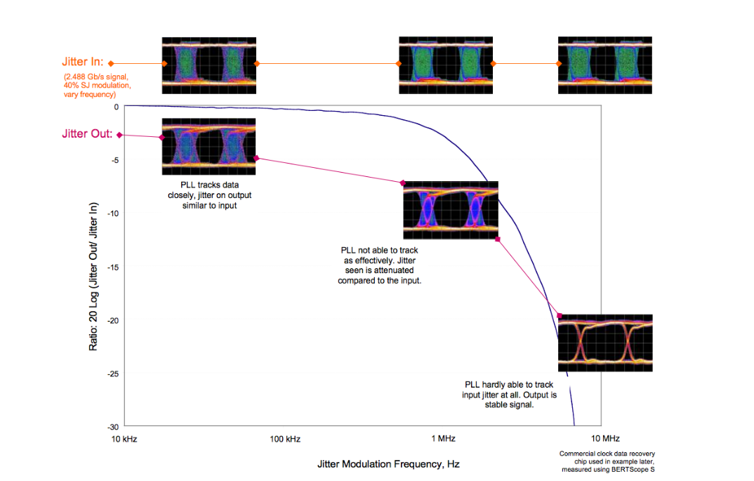
A measured loop response is shown in Figure 4.
- One measure of the jitter tracking characteristic of a PLL is the loop bandwidth (LBW). This is often measured as the point where the transfer function of (jitter out/jitter in) is –3 dB. This is not the only way that loops can be defined.
- A wide loop bandwidth sounds ideal. However, it is usually cost and technology dependent. Wide loop bandwidths contribute more noise/random jitter. A wide loop bandwidth improves jitter tolerance; a narrow loop bandwidth removes more jitter from the recovered clock (beneficial to downstream synchronizers) but impairs jitter tolerance.
- Current loop bandwidths used in measurements are typically in the range from 1 to 10 MHz.
Examples
We are going to look at two examples of clock recovery measurements, one with a commercial clock recovery component (Section 4), the other with a commercial clock/ data recovery chip (Section 5). In each case, the classical method of test is to use sinusoidal jitter (SJ) and to change modulation frequency. Here we will keep the jitter amplitude constant throughout.
Example 1: Testing a 10 Gb/s Clock Recovery Circuit
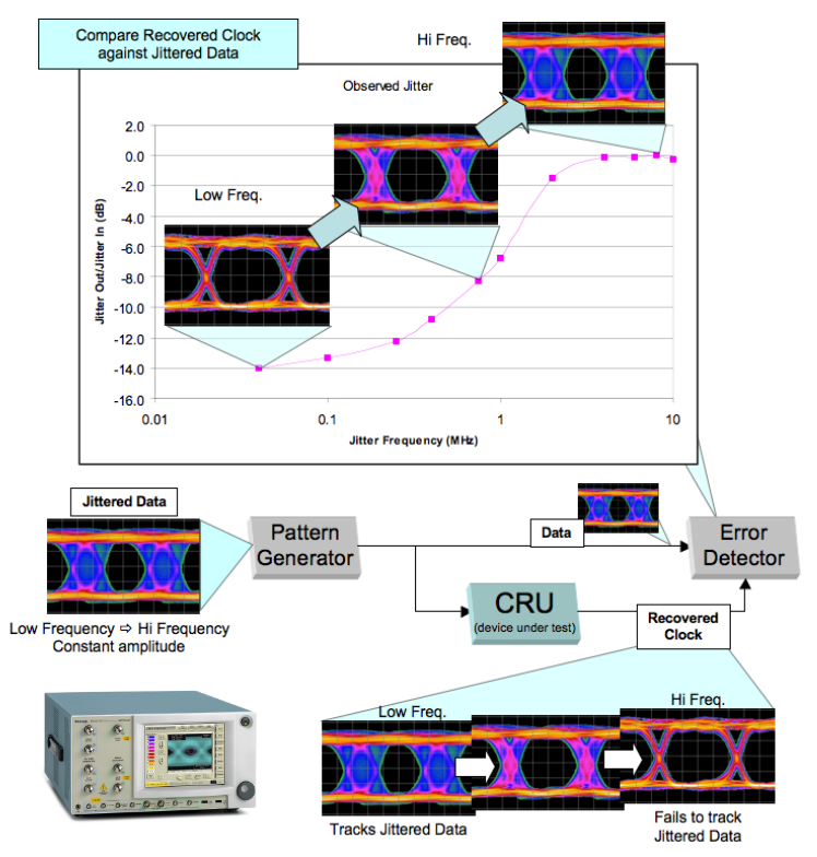
- Recovered clock is derived from jittered data
- Recovered clock tracks less and less jitter as the frequency of jitter on the data is increased
- Recovered clock is compared against jittered data in the analyzer
- The analyzer measures jitter relative to the clock trigger signal
- In this way, we can measure the clock recovery error transfer function
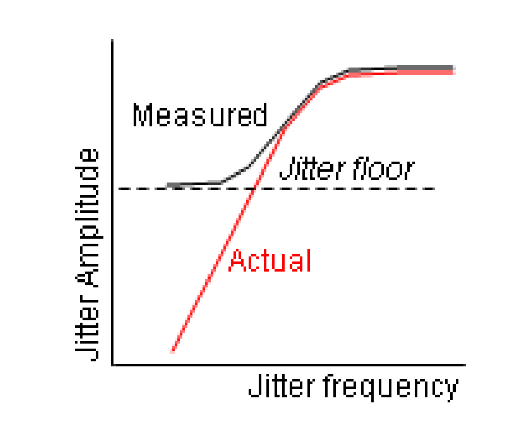
- Wideband equipment, such as BERTs and oscilloscopes, has intrinsic jitter that masks the loop responses at low levels in measurements such as this. As we will see later, the portions of loop responses not visible here can still have significant effects, manifesting themselves as eye closure and bit errors in some situations.
Example 2: Behavior of a Clock Data Recovery (CDR) Circuit
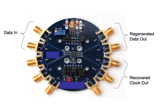
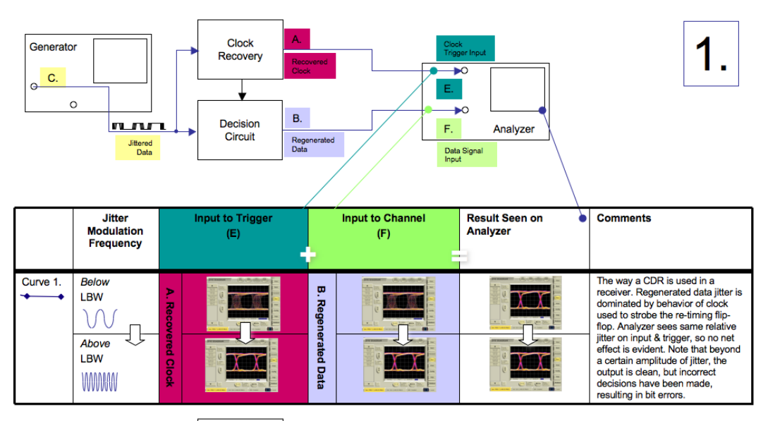
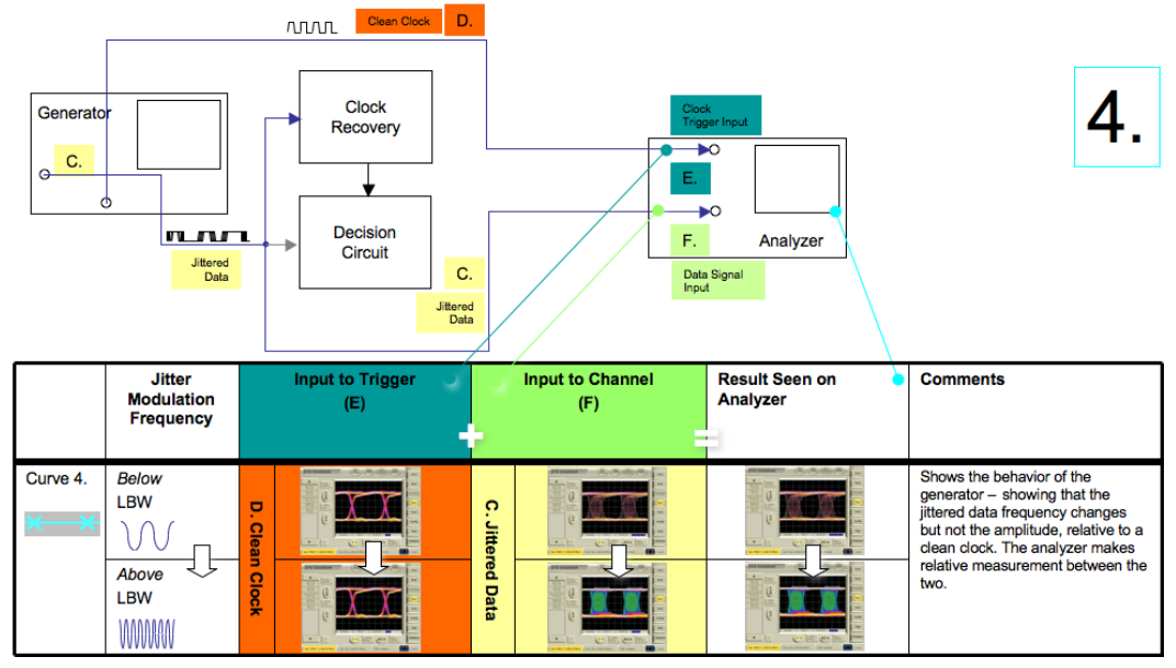
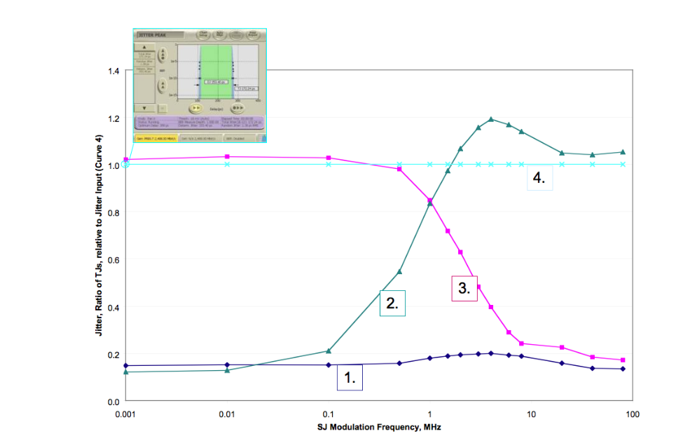
A CDR recovers clock from incoming data, then uses the recovered clock as the reference to trigger a retiming flipflop to clean up the incoming data. This measurement setup used a commercially available clock data recovery chip tested at 2.488 Gb/s, with a PRBS-7 pattern and 40% (0.4 UI) Sinusoidal Jitter signal of varying modulation frequency. The amplitude is constant; only the modulation frequency is varied, in the same way receiver clock recovery is traditionally tested. All analyzer measurements show data signal relative to the trigger.


Conclusions for Example 2
- Recovered clock jitter below the loop bandwidth tracks the input jitter
- Recovered clock jitter above the loop bandwidth is attenuated, so the recovered clock does not track high frequency jitter
- Jitter of retimed data is dominated by the jitter of the retiming clock
- High frequency jitter on incoming data can be of sufficiently high amplitude to cause bit-detection errors, even though the retimed, regenerated data stream appears clean on an analyzer screen
- Triggering of test equipment plays a crucial role in the results obtained
Where Does Clock Recovery Appear in Measurements?
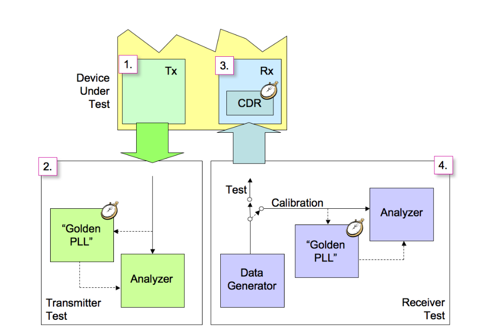
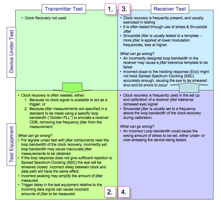
Clock recovery can be part of the device under test, and also of the test setup. Typically, when it is part of the test setup, it is intended to emulate the behavior of a receiver, particularly in tracking low frequency jitter. Ideally, this means that only jitter beyond the clock recovery tracking range of a typical receiver is seen on the test equipment eye diagram.
Loop Bandwidth Setting in Measurements
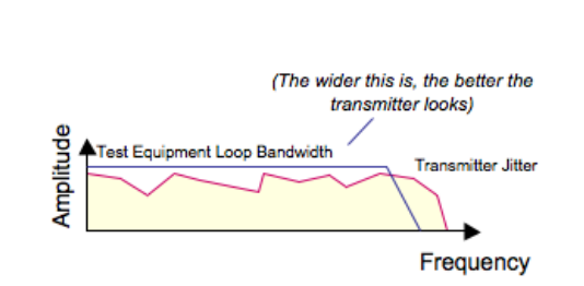
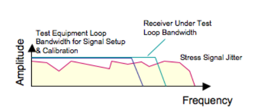
Loop bandwidth can have a significant effect on the observed jitter in a measurement. Varying the loop bandwidth can give an indication of the jitter spectrum. The loop bandwidths chosen for testing could be very narrow (for example, to show all the jitter a transmitter under test is creating) or wide (for example, to show only the jitter that a transmitter produces that its intended system receiver is not able to filter out with its own PLL). Typically, it is the latter, and such a clock recovery is referred to as a “Golden PLL.” A system designer is mainly interested in jitter that is beyond the capabilities of the receiver to track.
Some standards (like FB-DIMM) have a range of loop bandwidths specified. While test instruments should emulate the characteristics of the test device, a range in parameters could lead to unintended results.
- For transmitter testing, it might be desirable to have a high loop bandwidth to make the tested transmitter look as good as possible (the transmitter intrinsic jitter is largely tracked out, so it doesn’t appear in the measurement, making the transmitter look good).
- For receiver jitter tolerance, the stressed eye is often set up using jitter measured on an eye diagram. The aim might be to stress the eye with jitter beyond the effect of the receiver clock recovery’s ability to track it out. If the clock recovery used for stress calibration has a lower loop bandwidth than the receiver under test will, some jitter will be included in the eye measurement that will be tracked out by the receiver. This could make the composition of the finished stressed eye less demanding than it should be.

The Effect of Peaking
Peaking is a region near the loop bandwidth where the jitter out of a clock recovery device can be greater than the jitter input. Standards often restrict the amount of allowed peaking. The reasons why this is done are evident from the following measurements.
- An instrument-grade clock recovery with configurable slope and peaking was used for this measurement
- Loop bandwidth was set to 1 MHz
- The stimulus was a fixed 400 kHz sinusoidal jitter input signal to the clock recovery
- The loop was set to 0 dB peaking (red measured response) and +3 dB peaking (green measured response).
- The eye diagram from the green response shows jitter gain - more jitter out of the device than was present on the input.
- 3 dB equates to a factor of 1.41.
- Confirms that jitter gain is indeed +3 dB: 35 ps input x 1.41 = 49 ps jitter output.
- Many standards restrict the amount of peaking allowed (see table on "Anatomy of Clock Recovery, Part 2" poster).
- Jitter gain, particularly in a repeatered system, is highly undesirable.
- Peaking increases the noise/random jitter.

The Effect of Transition Density and Anomalous Clock Recovery Behavior
We will look at two loop effects; the first relating the transition density of different patterns and how this affects clock recovery; the second, how locking can go wrong.
Pattern Effects
The pattern "101010…" has a transition density of 100% (every bit has a transition). PRBS patterns have an average transition density identical to a "1100" pattern i.e., 50%. Other patterns may have a lower transition density, or one that changes in certain sections of the same pattern (such as some sections of long PRBS patterns).
The number of transitions controls the amount of energy going into the clock recovery loop. The energy in the loop affects the loop parameters, including loop gain and loop bandwidth.Therefore changing patterns can alter the loop behavior.
Halving the transition density can have the effect of approximately halving the loop bandwidth for most loop designs. Some instrument grade clock recovery solutions calibrate loop bandwidth based on the measured transition density of the incoming data. Care must be taken some standards specify loop bandwidth at a particular transition density, and assume that the loop bandwidth will be different for measurements using the required test patterns
Anomalous Locking
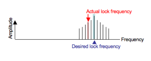
- Sidelocking
- Signals with periodic modulation produce discrete spectral lines
- Narrow band PLL can lock on to any sufficiently high amplitude discrete spectral line, whether the carrier or not
- Called 'sidelocking'
- Short PRBS patterns have fewer, higher energy spectral lines that are widely spaced, so can be more problematic than long PRBS patterns
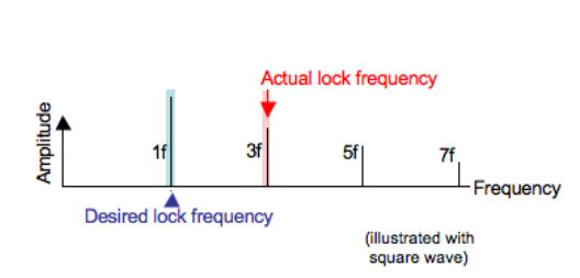
- Harmonic Locking
- Data, like square wave modulation, has harmonics that can provide opportunities to lock at multiples of the desired frequency
- This can also happen with some designs of phase detectors for subharmonics, and fractional subharmonics, particularly for long runs of ones or zeros.
These are some reasons why instrument clock recovery solutions usually require an initial frequency to be accurately established prior to acquisition.
Where to Go Next
In the same way that the second "Anatomy of Clock Recovery" poster tackles more complex topics, there is a companion second primer, "Anatomy of Clock Recovery, Part 2," which can be downloaded from the www.tektronix.com website.

