Introduction
As electrical power consumption continues to evolve in our industries, more power is required to be effectively converted in different ways. The power MOSFET (Metal Oxide Semiconductor Field Effect Transistor) is a key component in power conversion technology due to being well suited for very high voltage, high current, and high speed switching applications. These advantages promote further development in structure and material of new conversion technologies. A lot of materials and structures have been introduced to push existing boundaries in support of greater power and speed. Wide band gap materials silicon carbide (SiC) and gallium nitride (GaN) have been used prevalently in power MOSFET device technologies, and work in tandem with Keithley’s variety of high power source measure units (SMUs) to characterize the power MOSFET. The 2657A High Power System SourceMeter® Instrument covers 3 kV, and the 2651A — another high-power system SourceMeter® instrument — covers 50 A in pulse. The KickStart software offers the I-V Characterizer app that is used to establish automated setups and execution of I-V characterization tests for power MOSFET devices. This application note will provide details for how the power MOSFET I-V characterization is performed with a combination of the 2651A, 2657A, and 2636B System SourceMeter®Instruments and the KickStart Instrument Control Software.
Wide Band Gap Materials
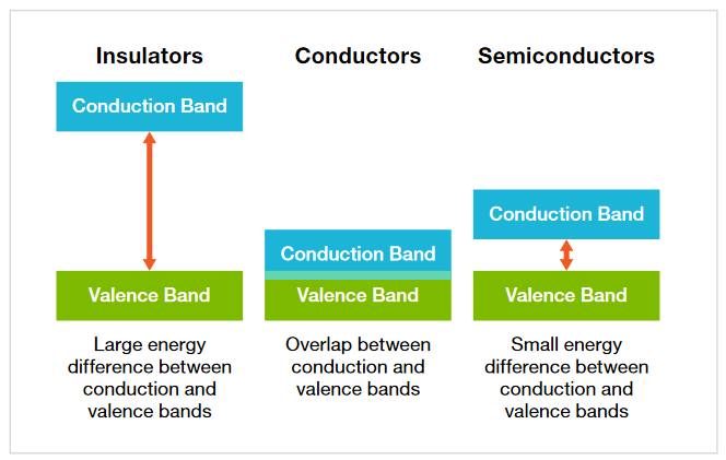
The electron is a key factor of electrical mobility and allows currents to flow – every individual material in this world has some energy level for electrons. As atoms are combined in solid state, the energy levels shown start to present as distinct ranges. The energy band of the electrons in the valence shell is called the valence band and these electrons cannot contribute to the current flow because they are bound to the valence band. However, if these electrons get some energy, electrically or thermally, they become excited and may shift to the conduction band where they are free to move and contribute to the current generation. The energy between the valence band and the conduction band is called the energy band gap.
Figure 1 shows if any material has a band gap of 1 eV to 3 eV that can move to the conduction band from valence band, those materials can be defined as semiconductors. If the material is higher than 5 eV, it is an insulator that prevents or severely minimizes electrical conductivity. Conductors can also be defined as two overlapped bands in which free electrons are always present even without acquiring any energy. Silicon has about a 1 eV band gap. When the band gap is larger than 2 eV, it is generally deemed a wide band gap device. SiC and GaN commonly use these wide band devices that have slightly more than 3eV band gap. Both materials have a high electric field so that they can block the larger voltages that regular silicon cannot. The electron in the n-type MOSFET is a majority carrier, and power MOSFETs utilize the advantage of these majority carriers to a conduct higher current. These wide bandgap materials also have advantages in thermal characteristics and electron mobility.
Power MOSFET Device Structures
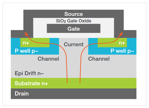
Figure 2 shows the basic device structure of a high power MOSFET. The drain is in the bottom of the wafer and the source on the top of it, making for a vertical structure. There are two p-n junctions in the left and right side. These junctions develop depletion layers so that in an off-state mode, the depletion layer expands in the drift region. This expanded layer can block very high voltage from the p well channel all the way to the drift layer.
In on-state mode, the channel region is formed by the gate voltage higher than the threshold value. It creates an inversion channel under the gate oxide that supports current flow from the drain to the source. Most regular low power MOSFET devices use some part of minority carriers, diminishing the device performance. When the channel is opened, the drift layer works as JFET (junction field emission transistor) so that a vest of majority carriers can move through the drift layer. This structure can have a very high current when in the on-state, and high voltage when in the off-state with high speed in switching either of these two states.
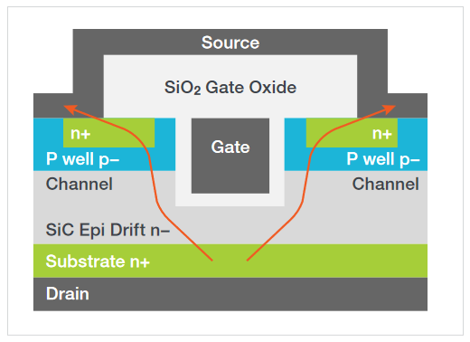
Other technologies have been introduced to improve device performance. Figure 3 shows one of these advanced structures: a trench MOSFET. There is a trench in the wafer hosting, the gate terminal and, the channel in the p well is formed vertically. There are some people who would prefer the drift layer thickness to increase to achieve a higher blocking voltage, however, the on-state resistance would then also increase with the thicker drift layer. Keeping the distance from the channel, to the drain short helps to keep the on-state resistance low. The trench structure MOSFET has very low on-state resistance — on the order of singledigit milliohm levels — due to the short drift layer.
Power MOSFET Test Setup
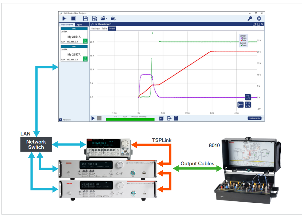
The 2657A High Power System SourceMeter®Instrument can support high voltage of up to 3 kV with a maximum current 120 mA. The 2657A is fit for the off-state measurement of power MOSFET devices in tests such as breakdown voltage and leakage current. The alternate High Power System SourceMeter® Instrument 2651A can support high current of up to 50 A at the maximum pulse level. It is good for on-state measurement tests like onstate resistance, conductance, output characteristic test,body diode, and transfer characteristic testing. The 8010 High Power Device Test Fixture is highly recommended for safe and reliable connections to the MOSFET under test. The KickStart software supports both High Power System SourceMeters 2657A and 2651A, as well as the 2636B. Each SMU should be connected to the control PC so the KickStart software can recognize each individual instrument. All three SMUs should be tethered together using the TSP-Link interface to enable the most efficient pulse testing through tight hardware triggering.
On-State Characterization
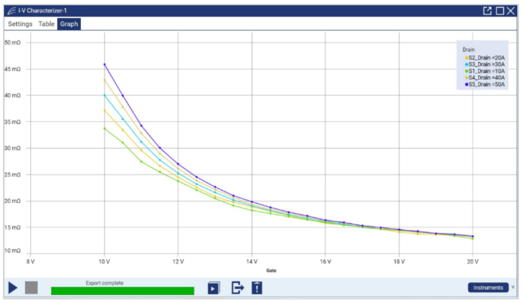
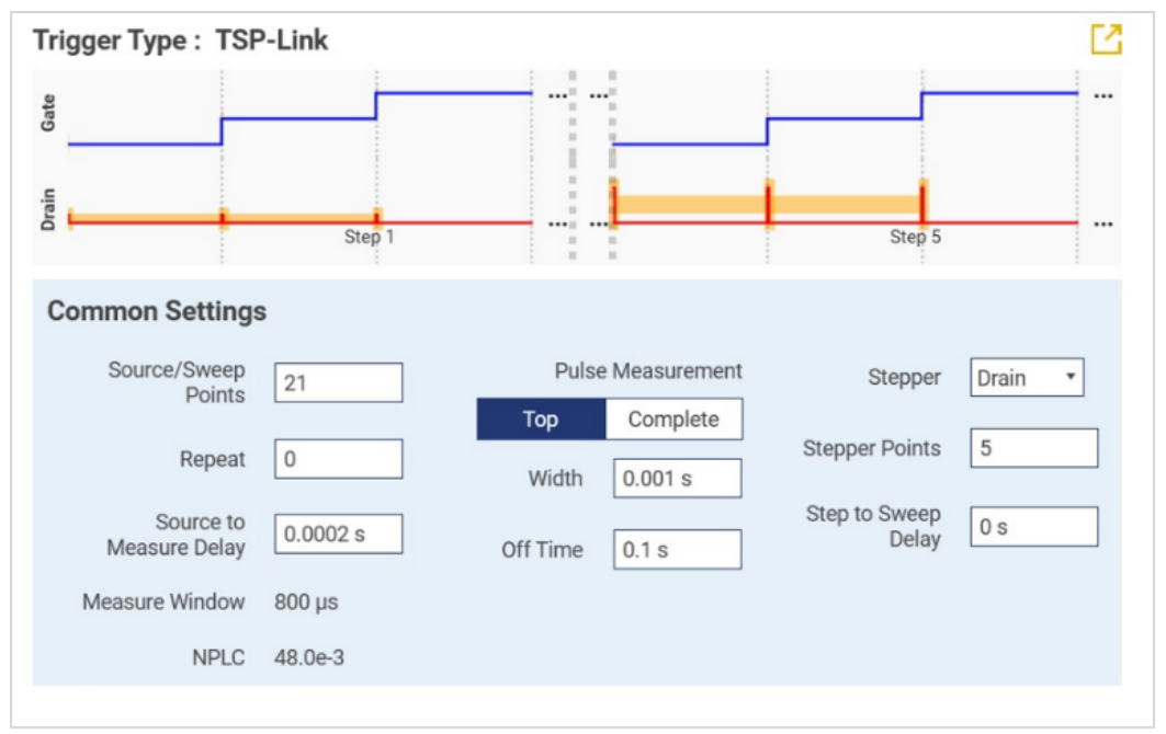
The on-state resistance (Rdson) is a key determinant of the conduction loss of a power MOSFET. As Figure 4 shows, its value can range from a few milliohms to tens of milliohms. The resistance of the drift layer contributes to the on-state resistance, and the thickness of the layer can affect the on-state resistance and breakdown voltage: the thinner the layer, the smaller the on-state resistance and the lower the breakdown voltage. The trench structure is helpful in reducing the on-state resistance, but it presents a tradeoff because a reduction in the breakdown voltage will likely lead to an increase in the on-state resistance. The test condition of the on-state resistance is usually defined as a resistance measured at a specific current level of the drain and specific voltage bias of the gate. Figure 4 shows the on-resistance measurements with some drain current steps from 10 A to 50 A while sweeping the gate voltage from 10 V to 20 V. The on-state resistance is about 14 mΩ with the device drain pulsed at 50 A of current with 20 V applied to the gate. The 2651A SourceMeter supports 1ms maximum pulse width in the 50 A range at 10 V. If the higher voltage ranges of 20 V or 40 V are required, then the maximum pulse width will reduce to 330 µs and 300 µs, respectively. KickStart will provide a pulse or output signal preview for each terminal (Figure 5).
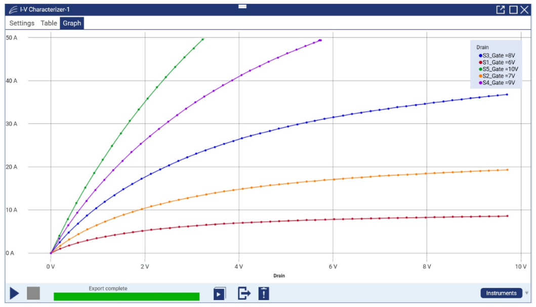
Another important test in the on-state is the output characterization as shown in Figure 6. This test sweeps the drain voltage from 0 V to 10 V with the gate stepping from 6 V to 10 V in 1V increments. This high current test must be done with as short a pulse width as possible to avoid thermal heating.
Off-State Characterization
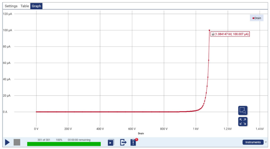
The off-state breakdown voltage (BVDSS) is another important parameter of the power device, helping to determine the maximum voltage that can be applied to it. If the p well channel is closed, the device is like a p-n junction, where positive drain voltage becomes the reverse bias to the p-n junction creating more voltage and drift layer depth to maintain the blocking of the voltage levels. The BVDSS is usually defined as the drain to source voltage when the leakage current is set to approximately 100 µA while the gate bias is 0 V. The BVDSS measurement can be performed by measuring voltage while sourcing current at a specified leakage level. Another method is to sweep the voltage across the drain using a current compliance set to the leakage level. In either test method, the gate bias is 0 V to ensure the device is in its off state. At the point where the current hits the compliance level, the corresponding voltage is interpreted as the breakdown voltage. Figure 7 shows the result sweeping from 0 V to the 1.5 kV. The current hits the 100 µA compliance at 1.08 kV, therefore, the breakdown voltage BVdss is said to be 1.08 kV.
Body Diode Characterization
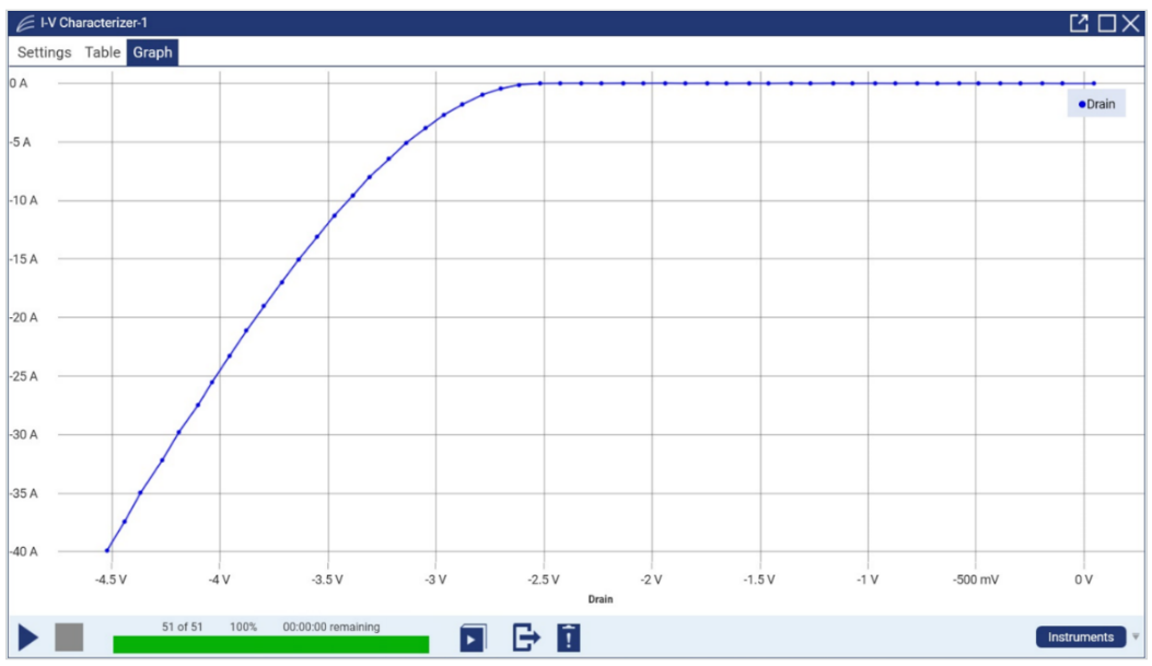
There is a body diode characteristic in some power MOSFET datasheets. The p-type layer is shorted to the source, and it faces the n-type drift layer so that a p-n diode is formed between the source and the drain (as shown in Figure 2),causing current to flow in the reverse direction. This is not the expectation for the power MOSFET design, but this feature can be used in some analog circuits.Figure 8shows that KickStart can make the body diode measurement by sweeping the drain voltage from 0 V to –5 V with the gate voltage biased to –5 V.
Conclusion
Power MOSFET devices have different technologies depending on device structure, materials, and operation principle, and as any of these characteristics change, DC I-V characterization will need to be done. The two most critical power MOSFET parameters are the on-state resistance and off-state breakdown voltage. The Keithley High Power System SourceMeter® Instruments and the Keithley KickStart software are great solutions that allow users to achieve the DC characterization of their devices quickly and easily
Find more valuable resources at TEK.COM
Copyright © Tektronix. All rights reserved. Tektronix products are covered by U.S. and foreign patents, issued and pending. Information in this publication supersedes that in all previously published material. Specification and price change privileges reserved. TEKTRONIX and TEK are registered trademarks of Tektronix, Inc. All other trade names referenced are the service marks, trademarks or registered trademarks of their respective companies.
110122 1KW-73967-0

