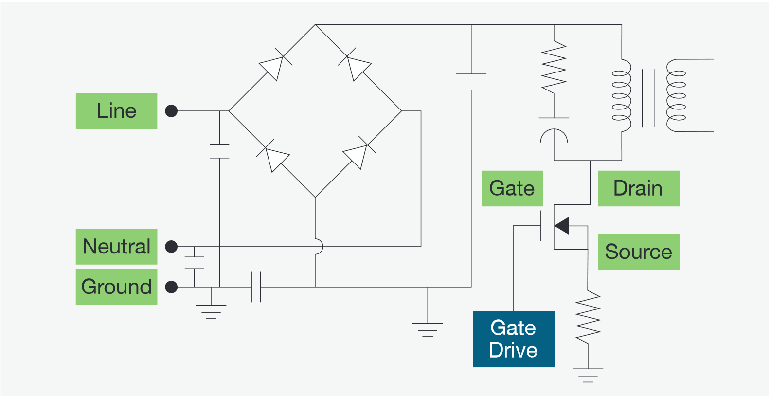
Power supply design is a delicate balancing act, with the engineer trading off electrical performance and specifications, size, weight, cost, heat, EMI/EMC compatibility, and reliability to optimize the design. One of the key electrical components is the switching device, and it is critical that it always operate within its specifications to prevent degradation of its reliability
This application note gives six steps for taking high-quality parametric measurements on the output of a switching device, and describes three methods for using an oscilloscope to determine whether a MOSFET or other switching device is operating within its specifications:
- A visual spot check: a quick check but not practical for testing over a range of operating conditions
- Using Limit Test to check a single parameter for specification violations
- Automated safe operating area (SOA) analysis that simultaneously monitors multiple parameters
The last technique plots measurements on a safe operating area oscilloscope display. SOA graphs are commonly provided in MOSFET datasheets to describe the maximum voltage, current, and instantaneous power ranges of a particular device.
Differences between Ideal and Real Switching Devices
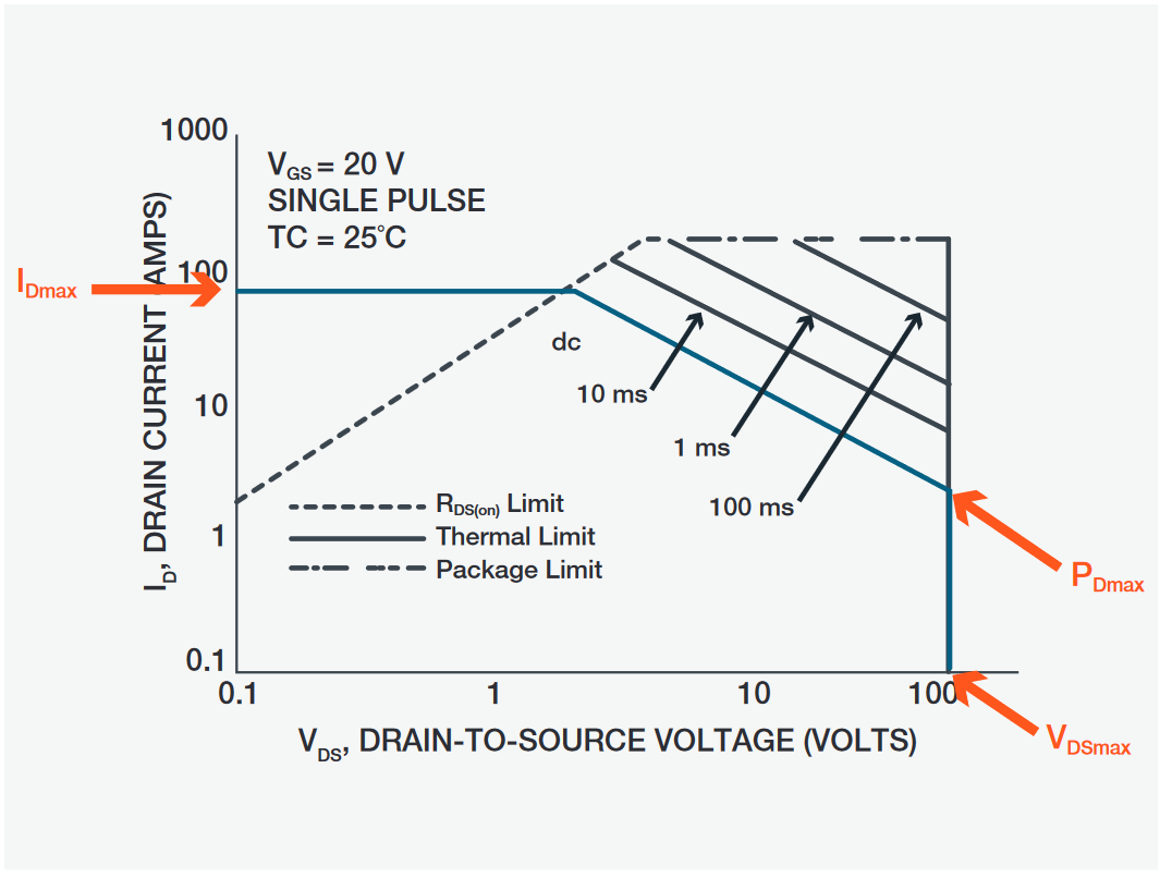
An ideal switching device is either “on” or “off” like a light switch, and instantaneously switches between these states. In the “on” (conduction) state, the impedance of the switch is zero and no power is dissipated in the switch, no matter how much current is flowing through it. However, real switching devices have some inherent resistance in the on state as well as current limits associated with physical constraints such as bond wires. Thus switching devices have a maximum rated current: I Dmax in the case of a MOSFET or ICmax in the case of an IGBT or BJT. The current through the switch must never exceed this maximum value.
In the “off” state, the impedance of the switching device is infinite and zero current is flowing, and no power is dissipated, no matter how high the voltage. Real switching devices have a maximum rated voltage, V DSSmax for a MOSFET or VCEmax for an IGBT or BJT, and the voltage across the switch must never exceed this maximum value.
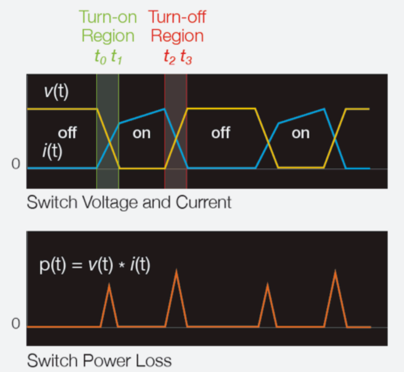
Power dissipation during the ON and OFF states is typically very low. However, significantly more power is dissipated during the transitions between “on” and “off” (turn-off) and between “off” and “on” (turn-on) as the switch very briefly passes through its linear region. The instantaneous power can be calculated by multiplying the voltage across the switch by the current flowing through the switch. This maximum power dissipation, PDmax, must never exceed the maximum specification found in the component data sheet.
Six Steps to High-quality Switch Measurements
1. Ensure accuracy and safety. For best accuracy, be sure to use the equipment within the normal operating range and below the peak ratings. And, for your safety, always stay well within the equipment’s absolute maximum specifications and follow manufacturer’s instructions for use.
2. Remove offset errors in voltage measurements. The amplifiers in differential probes may have a slight DC voltage offset which will affect measurement accuracy. With the inputs shorted and no signals applied, automatically or manually adjust the DC offsets in the probe to zero.
3. Remove offset errors in current measurements. Current probes may exhibit DC offset errors due to residual magnetism in probe, as well as amplifier offsets. With the jaws closed and no signals applied, automatically or manually null out the DC offsets in the probe.
4. Remove timing errors. Different technologies are used to measure voltages and currents, and the propagation delays through these devices may be significantly different, leading to measurement errors in instantaneous power. For the most accurate results, apply a high-slew-rate signal to all inputs and use the deskew menu to carefully remove any relative timing offset (skew) between all channels.
5. Optimize Signal-to-Noise Ratio. In all measurement systems, but especially in digital devices such as modern oscilloscopes, good measurement technique requires keeping signals as large as possible (without clipping) to minimize the effects of noise and to maximize vertical resolution. Use the lowest necessary attenuation when probing the signals to take advantage of the full dynamic range of the oscilloscope.
6. Add signal conditioning. Measurement quality can be improved by conditioning the input signals. Bandwidth limiting can be used to selectively reduce noise above the frequencies of interest, and averaging can be used to reduce uncorrelated or random noise on the signal. HiRes acquisition mode, a type of box-car averaging, provides bandwidth limiting and noise reduction, increased vertical resolution, and it even works on single acquired signals.
Making Spot-checks of Voltage, Current and Power on a Switching Device
The switch voltage, current, and instantaneous power can be displayed on the oscilloscope and quickly compared to datasheet maximums. (For detailed steps for taking these measurements, see “Six Steps to High-quality Switch Measurements”.) Figure 3 shows the measurements on the output of a typical MOSFET. The MOSFET’s V DS is acquired with a differential voltage probe and is shown in yellow. The drain current is acquired with an AC/DC current probe and is shown in cyan. The vertical sensitivity and offset of each channel is adjusted so the signals occupy more than half of the vertical range, but without extending beyond the top and bottom of the graticule.

A stable display is important for visual analysis, so the oscilloscope’s edge trigger is set to the 50% point on the voltage waveform. Then the sample rate is set to assure adequate timing resolution on the signals’ edges. In this case, a sample rate of 10 MS/s results in many sample points on each edge of the switching waveform. Finally, HiRes acquisition mode is enabled to reduce the signal bandwidth to about 4.4 MHz and increase the vertical resolution to about 12 bits. Waveform math is then used to multiply the current by the voltage to create the orange instantaneous power waveform.
Using measurements like the one in Figure 3 makes it possible to do quick spot-checks to determine if the voltage, current, and power are exceeding the maximums set forth in the component datasheet at a particular instant. However, such a manual measurement technique is time-consuming, errorprone, and very difficult to do while the power supply is tested throughout its full operating range.
Using Limit Test for Single-Parameter Monitoring
Many oscilloscopes can monitor a signal and automatically catch any violations of a single maximum specification. Figure 4 shows an example of an oscilloscope feature called Limit Test. Using Limit Test an oscilloscope can monitor the IDS through a MOSFET, for example, and signal the user if the test limits are ever violated. (For example, the oscilloscope can beep, email the user, capture the waveforms, stop acquisitions, etc.)
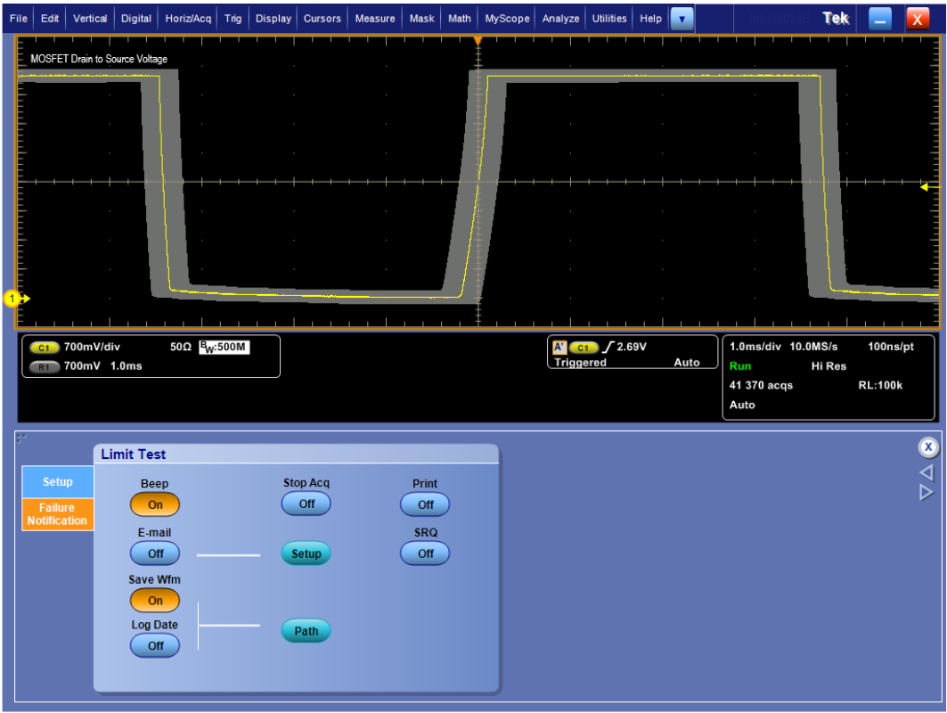
Using limit test is preferable to performing quick visual checks, since the test can run for long time periods, during which the operating environment may be varied to simulate real world conditions. This technique can catch many violations of component specifications, however, it is limited to a single parameter at a time.
Automated Safe Operating Area Analysis
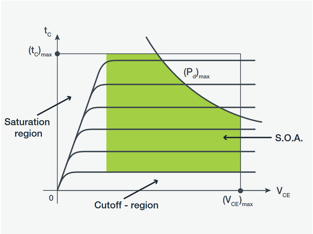
Safe Operating Area (SOA) is found in device datasheets. It is a graphical representation of the devices maximum operating current and voltage at DC and various pulse widths, at a specified temperature.
Tektronix Power Analysis options provide a way to evaluate actual circuit operation against an SOA graph. This provides a very simple graphical method for monitoring the interactions between voltage and current as conditions are varied to simulate the range of operation of a power supply.
The underlying display is a simple X-Y display, such as the one in Figure 7, with the switch voltage on the horizontal axis and the switch current on the vertical axis.
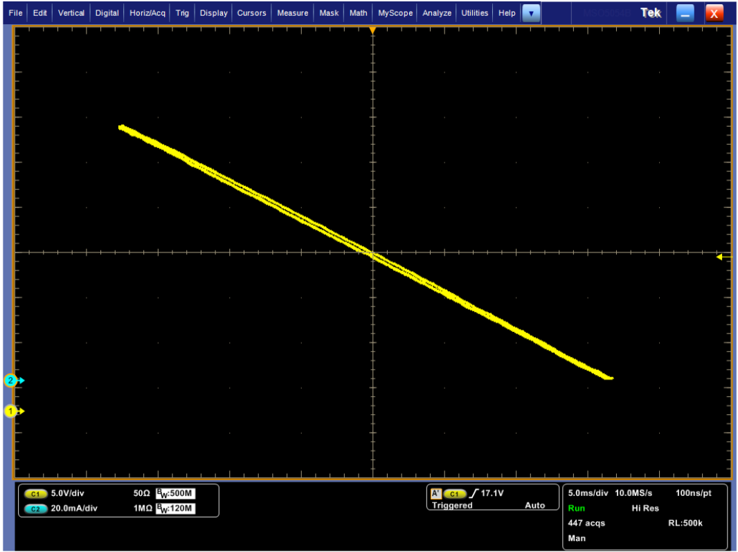
Automated SOA analysis combines the X-Y display, plotted on a log-log scale, with automatic limit/mask testing, to build a representation of the SOA graph on the oscilloscope display, as shown in Figure 8. This allows switch voltage, current, and power to be simultaneously and automatically monitored as operating conditions vary.
For the MOSFET example shown in Figure 8, the SOA mask was generated from these key maximum specifications:
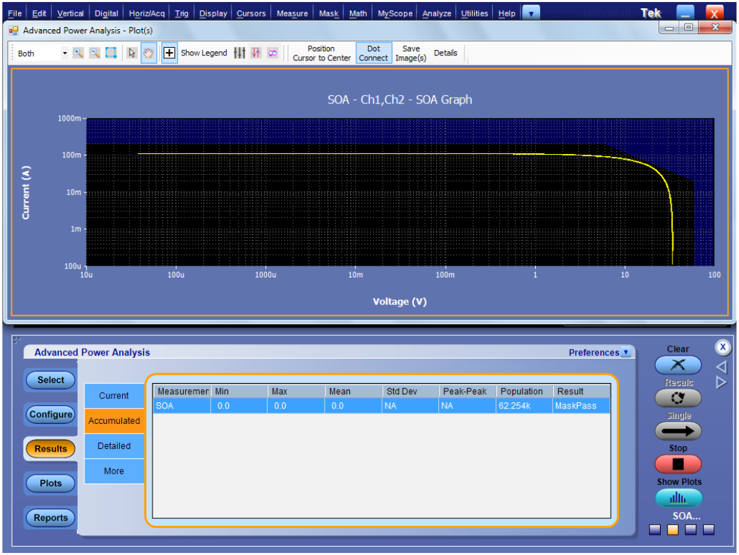
- VDSmax = 60 V
- IDmax = 200 mA
- PDmax = 1.25 W
The oscilloscope continuously compares the X-Y waveform to the SOA mask. When automated SOA analysis detects an error, the mask test will highlight the waveform points that violated the mask and the pass/fail indicator will indicate an error has occurred, meaning that the switching device is operating outside of its absolute maximum ratings. This type of automated measurement is especially valuable for remote testing and when running tests outside of office hours.
So, why are reliable and repeatable measurements so important? Thorough power supply testing should include SOA testing of the switching device or devices over the full range of operating conditions, including full input voltage range, full output load range, dynamically changing load, temperature range, altitude range, humidity range, and so on. Imagine trying to manually monitor the switching device while all of these tests are being done!
Safe Operating Area measurements are a critical part of verifying the design and assuring the reliability of switch mode power supplies. By using good measurement techniques and automating the power measurements, it is easy make simultaneous voltage, current, and instantaneous power FIGURE 8. SOA mask testing within oscilloscope power application. measurements, quickly and repeatably.
MEASUREMENTS SHOWN IN THIS APPLICATION NOTE WERE MADE WITH THE FOLLOWING TEST EQUIPMENT:
- MSO5204B Mixed Signal Oscilloscope
- DPOPWR Advanced Power Analysis Application
- TDP1000 1 GHz differential probe
- TCP0030A 120 MHz AC/DC current probe


