Contact us
Call
Call us at
Available 6:00 AM – 5:00 PM (PST) Business Days
Download
Download Manuals, Datasheets, Software and more:
Feedback
TLA7SA00 PCI Express Logic Protocol Analyzer Datasheet
TLA7SA00 Series Datasheet
The products on this datasheet are no longer being sold by Tektronix.
View Tektronix Encore for reconditioned test equipment.
Check support and warranty status for these products.
TLA7SA00 Series Datasheet
The TLA7SA00 Series logic protocol analyzer modules provide an innovative approach to PCI Express validation that spans all layers of the protocol from the physical layer to the transaction layer. Feature rich software provides improved information density for viewing statistical summary and protocol analysis using innovative Transaction and Summary Profile windows. Hardware capabilities including hardware acceleration, OpenEYE, ScopePHY, and FastSYNC provide fast access to data and helps shorten the time it takes to build confidence in the test system. Powerful trigger and filtering capabilities provide the ability to quickly focus on the data of interest. A complete suite of probing solutions targeted for various form factors and applications.
Notice to EU customers
This product is not updated to comply with the RoHS 2 Directive 2011/65/EU and will not be shipped to the EU. Customers may be able to purchase products from inventory that were placed on the EU market prior to July 22, 2017 until supplies are depleted. Tektronix is committed to helping you with your solution needs. Please contact your local sales representative for further assistance or to determine if alternative product(s) are available. Tektronix will continue service to the end of worldwide support life.
Key performance specifications
- PCI Express Gen1, Gen2, and Gen3 Protocol to Physical Layer Analysis for link widths from x1 through x16 with up to 8.0 GT/s acquisition rates.
- Industry's deepest 8 GB memory/module (16 GB memory, x16 link width) increases the chances of capturing an error and the fault that caused the error.
Key features
- Comprehensive PCI Express probing solutions, including midbus, slot interposer, and solder-down probes.
- Nonintrusive probing that uses OpenEYE technology incorporating automatic tuning equalization circuitry to allow probing anywhere on the channel and ensures accurate data capture in PCI Express systems with channel lengths up to 24 in. and two connectors.
- Single-click calibration process calibrates the analyzer and probes to the target BER. Calibration results for analyzer/probe sets are remembered from one session to another.
- ScopePHY provides the ability to quickly connect any of the PCI Express midbus, slot interposer, or solder-down probes to a high-performance oscilloscope providing a more detailed analog view of the PHY Layer.
- Shorten time to gain confidence in the test system setup.
- Front-panel LEDs provide status information such as link speed, symbol lock, and link activity.
- Auto-configure sets up the logic protocol analyzer system to be ready for data acquisition quickly.
- FastSYNC tracks the Link as it transitions in and out of ASPM Power states such as L0s, regardless of electrical Idle duration.
- Real-time statistics help observe link health and behavior over time.
- Powerful trigger-state machine spans all layers of the protocol.
- 8 States
- 8 Packet recognizers
- 4 Symbol sequence recognizers
- 4 Counter/Timers
- 4 Event flags
- Conditional storage
- Real-time filtering
- HW accelerated search and data displays provide immediate visibility of data regardless of record length.
- Information density for rapid data analysis
- The Transaction window provides visibility into protocol behavior at the packet and transaction level interspersed with physical layer activity.
- Innovative Bird's Eye view provides a high-ground visibility of system issues involving flow control.
- The Summary Profile window helps ascertain the health of the system and identify patterns of interest such as errors, TLPs, DLLPs, ordered sets.
- Multibus visibility for system-level debug
- Analyze complete system interactions with time-correlated, multibus analysis on a single display on a single mainframe. For example, tracing memory access from PCI express to DDR memory or monitor multiple PCIe links on a PCIe switch.
- Cross Triggering and a common global time stamp enables accurate and efficient debugging by showing exactly what was happening on one bus relative to another at any given instant in time.

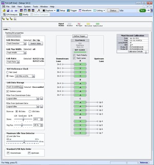
The TLA7SA00 series logic protocol analyzer Setup window provides a quick overview of link connection status.
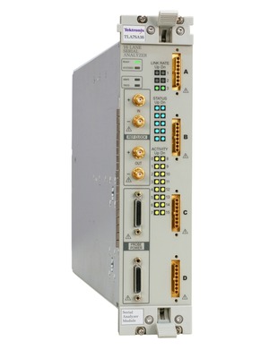
TLA7SA16 Logic Protocol Analyzer module.
Applications
- PCI Express debug from Protocol layer to Physical layer
- Silicon validation
- Computer system validation
- Embedded system debug and validation
- Processor/Bus debug and verification
- Embedded software integration, debug, and verification
PCI Express debug and analysis spanning Physical to Transaction-layer with feature-rich hardware
PCI Express 3.0 introduces new challenges for validation engineers. Time-to-market pressures require a solution that can quickly pinpoint problems. The TLA7SA00 Series logic protocol analyzer modules provide an innovative approach to PCI Express validation that spans all layers of the protocol from the Physical layer to the Transaction layer.
Reduce the time to information by viewing and searching up to 16 GB deep memory in just seconds with rapid display updates enabled by our industry-leading hardware acceleration.
Features such as auto-training, auto-tracking, front-panel LED lane status, single-click calibration, allow the logic protocol analyzer to "wire" itself automatically which shortens the time it takes for users to build confidence in the test system.
Quickly trigger on patterns of interest with powerful trigger capabilities that span across all protocol layers. Real-time filtering provides the ability to filter unwanted data and use the acquisition memory more efficiently by storing only transactions of interest.
Elusive power state anomalies pertaining to entry into and exit from electrical idle and ASPM states such as L0s to L0 are easily addressed by FastSYNC technology. It ensures quick re-synchronization of the logic protocol analyzer with the PCI Express FTS ordered sets regardless of the duration of electrical Idle time. This capability is unique compared to other solutions where the L0s to L0 re-synchronization time is specified only over a short electrical idle time of 2 μs or less.
Innovative data displays for accelerated time to information
The new PCI Express software helps view information in a hierarchical and rich format. Protocol information can be expanded and collapsed to rapidly display or hide information as needed.
Quickly ascertain the health of the system and identify patterns of interest (errors, specific transactions, ordered sets) with statistical summary and data graphs using the Summary Profile window. Summary statistics include useful information such as average transaction latency, total bytes transmitted, and bus utilization.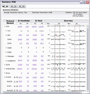
Summary Profile window
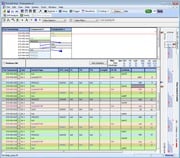
Protocol behavior can be viewed at the packet and transaction level interspersed with physical layer activity in a single innovative Transaction window. The Transaction Stitching feature shows packets participating in a completed transaction or incomplete transactions as errors in a diagrammatic representation. Additional capabilities, including color coding of the packets, cursor locking across multiple data windows, and a unique Bird's Eye view integrated with the Transaction window provides a high-ground visibility of system issues involving flow control.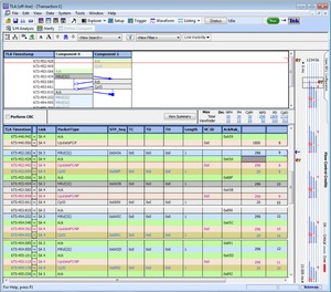
Transaction window with integrated Bird’s Eye view
Further insight into physical layer details can be gained with the unique Listing window showing packet details and lane-by-lane symbol decode. You can also view individual lane activity correlated with analog waveforms from your high-bandwidth oscilloscope in the Waveform window.
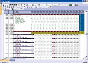
Listing window showing packet details and lane-by-lane symbol decode
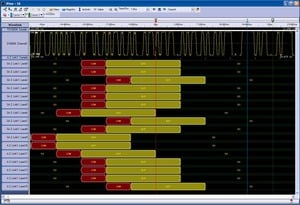
Waveform window showing individual lane activity correlated with analog waveform
Hardware developers, hardware/software integrators, andembedded system designerswill appreciate the tight integration with the Tektronix logic analyzer. This provides visibility of complete system interactions with time-correlated, multi-bus analysis on a single display. Cross triggering and a common global time stamp enables accurate and efficient debugging by showing exactly what was happening on one bus relative to another at any given instant of time.
High-performance PCI Express probing solutions for different application needs
The P67SA00 Series probes provide validation engineers with a comprehensive set of PCI Express probing solutions, including midbus, slot interposer, and solder-down connectors. With support for PCI Express Gen1, Gen2, and Gen3 channel lengths up to 24 in. with two connectors, these probes use OpenEYE technology offering minimal electrical loading with the highest signal fidelity and active equalization to ensure accurate data recovery of closed eyes. All P67SA00 Series probes feature a graphical lane-swizzling capability for maximum flexibility to accommodate unique circuit board layouts.
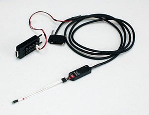
P67SA01SD – single differential input PCI Express solder-down probe, shown with Option 1P power adapter.
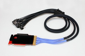
P67SA16S – x16 PCI Express Slot Interposer probe. (x8, x4, x1 Slot Interposer probes also available)
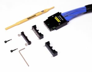
P67SA16 – x8 PCI Express Midbus probe and accessories. (x4 Midbus probe also available)
With ScopePHY, quickly connect any of the probe connector outputs to an oscilloscope using the P67UHDSMA probe lead set to gain further insight into the PHY layer. Tektronix-supplied S-parameters of the probe and module configure the DSP filters of Tektronix oscilloscope to show the PCI Express link data eye at the probe tip.
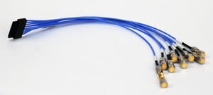
P67UHDSMA – x2 PCI Express probe lead set for P67SA00 probe connections to oscilloscopes.
Specifications
All specifications are guaranteed unless noted otherwise. All specifications apply to all models unless noted otherwise.
General specifications
- Acquisition rate with frequency margin
- 8 GT/s (+5% to -10%)
5 GT/s (±10%)
1.5 GT/s (±10%)
- Number of lanes
-
- TLA7SA08
- 8 differential inputs, x4
- TLA7SA16
- 16 differential inputs, x8
- Record length
- 160 M symbols translates into 160 ms at 8 GT/s, 320 ms at 5 GT/s, or 640 ms at 2.5 GT/s at 100% bus utilization.
- TLA7SA08
- 160 M symbols per differential input, 4 GB physical memory total
- TLA7SA16
- 160 M symbols per differential input, 8 GB physical memory total (16 GB physical memory for a x16 configuration)
- Time stamp range
- 292 hours
- Time stamp
- 50 bits at 936 ps resolution
- Clocking/acquisition modes
-
- TLA module without SSC (spread spectrum clocking)
- External reference clock
- 100 MHz ±10% with or without SSC
- External reference clock frequency tolerance
- ±300 ppm
- Number of mainframe instrument slots required per TLA series module
- 2
Module configuration requirements
- Bi-directional link widths per module
-
Module X1 X4 X8 X16 TLA7SA08 1 1 0 0 TLA7SA16 1 1 1 2
Input specifications (with P67SA00 series probes)
- Capacitive loading
- Please refer to the specifications in the Tektronix Logic Analyzer Solutions for PCI Express 3.0 manual, Tektronix part number, 077-0400-xx.
- Minimum data eye
- Please refer to the specifications in the Tektronix Logic Analyzer Solutions for PCI Express 3.0 manual, Tektronix part number, 077-0400-xx.
Acquisition system (with P67SA00 series probes)
- Dynamic link width switch latency
- Consumes up to 48 symbols (typical)
- Dynamic link rate switch latency
- <200 ns EIDLE time (typical) (with either internal reference clock or spread spectrum using external reference clock)
- Maximum time to change to Gen1 rate
- 2 TS1
- Maximum time to change to Gen2 rate
- 1 EIEOS + 3 TS1
- Maximum time to change to Gen3 rate
- 1 EIEOS + 6 TS1
- Number of FTS packets required to resync following L0s exit
- Assumes an EIDLE ranging from 20 ns to 2 ms, with either internal reference clock or spread spectrum using external reference clock
- Gen1
- 4 FTS (typical)
- Gen2
- 1 EIEOS + 6 FTS (typical)
- Gen3
- 1 EIEOS + 4 FTS (typical)
Filter specifications
- Ordered sets
- TS1, TS2, SKP, EIOS, FTS, EIEOS, SDS
- DLLPs
- Ack, Nak, PM, Vendor specific, FC1, FC2, UpdateFC
- TLPs
- MRd, MRdL, MWr, IORd, IOWr, CfgRd0, CfgWr0, CfgRd1, CfgWr1, Msg, MsgD, Cpl, CplD, CPlLk, CPlDLk, FetchAdd, Swap, CAS, LPrfx, EPrfx
Trigger system
- Independent Trigger states
- 8
- Trigger sequence rate
- Operates at symbol rate time (Gen1, Gen2, Gen3)
- Maximum independent If/Then clauses per state
- 8
- Maximum number of events per If/Then clause
- 8
- Maximum number of actions per If/Then clause
- 8
- Maximum number of event counters per state
- 2
- Event counter range
- 31 bit
- Number of TLP packet recognizers per link direction
- 4
- Number of DLLP packet recognizers per link direction
- 4
- Number of sequence recognizers
- 4
- Number of symbols per sequence recognizer
- 16
- Number of link event recognizers
- 4
- Number of global counters/timers
- 4
- Trigger event types
- Anything, TLP, DLLP, Sequence, Link Event, Counter, Timer
- Trigger action types
- Trigger, Trigger All Modules, Wait for System Trigger, Goto, Increment Counter, Decrement Counter, Reset Counter, Start Timer, Reset Timer, Reset and Start Timer, Stop Timer, Reset and Stop Timer, Set Signal Out, Clear Signal Out, Arm Module, Start Storage, Stop Storage, Do Nothing
- Counter/timer range
- 48 bit (~5 days with 3.6 ns resolution)
- Counter/timer test latency
- 68 ns
- Storage control (data qualification)
- By state (start/stop)
Physical characteristics
- Dimensions
-
- Height
- 262 mm (10.3 in.)
- Width
- 61 mm (2.4 in.)
- Depth
- 381 mm (15.0 in.)
- TLA7SA08 weight
-
- Net
- 2.84 kg (6.25 lb.)
- Shipping
- 6.94 kg (15.3 lb.)
- TLA7SA16 weight
-
- Net
- 3.20 kg (7.06 lb.)
- Shipping
- 7.30 kg (16.1 lb.)
PCI Express midbus differential data probes
- General
-
Characteristic P67SA08 P67SA16 P67SA16G2 Number of differential pairs 8 16 16 Lane width x4 x8 x8 Recommended use Recommended where signal integrity is critical Recommended where signal integrity is critical Recommended for midbus probing of PCIe Gen2 Attachment to target system Compression technology Compression technology - Probe loading AC/DC Refer to the Tektronix Logic Protocol Analyzer Solutions for PCI Express 3.0 Instruction manual, Tektronix part number 077-0400-xx. Cable length 1.8 m (6 ft.)
- Midbus probe recommended configurations
-
x1 x4 x8 x16 1 P67SA08 1 TLA7SA08 1 P67SA08 1 TLA7SA08 1 P67SA16 1 TLA7SA16 2 P67SA16 2 TLA7SA16
PCI Express slot interposer probes
- General
-
Characteristic P67SA04S P67SA08S P67SA16S Number of differential pairs 8 16 32 Lane width x4 x8 x16 Recommended use Recommended for platforms with no midbus footprints and the PCI Express slot is the only probe access point Attachment to target system PCI Express slot Probe loading AC/DC Refer to the Tektronix Logic Protocol Analyzer Solutions for PCI Express 3.0 Instruction manual, Tektronix part number 077-0400-xx. Cable length 1.8 m (6 ft.)
- Slot interposer probe recommended configurations
-
x1 x4 x8 x16 1 P67SA04S 1 TLA7SA08
1 013-0375-xx1 P67SA04S 1 TLA7SA08 1 P67SA08S 1 TLA7SA16 1 P67SA16S 2 TLA7SA16
PCI Express solder down and UHDSMA probes
- General
-
Characteristic P67SA01SD P67UHDSMA Probe type PCI Express differential solder-down probe Probe lead set for PCI Express P67SA00 series probe connections to high-bandwidth oscilloscopes Number of differential pairs 1 4 Lane width 1/2 lane x2 Recommended use Recommended for platforms with no midbus footprint, PCI Express slot; or where space is limited Recommended for use with any of the P67SA00 series probe connections to high-bandwidth oscilloscopes Attachment to target system Solder down - Probe loading AC/DC Refer to the Tektronix Logic Protocol Analyzer Solutions for PCI Express 3.0 Instruction manual, Tektronix part number 077-0400-xx. - Cable length 1.8 m (6 ft.) 0.3 m (1 ft.)
- Solder-down probe recommended configuration
-
x1 x4 x8 x16 2 P67SA01SD 1 TLA7SA08 8 P67SA01SD 1 TLA7SA08 16 P67SA01SD 1 TLA7SA16 32 P67SA01SD 2 TLA7SA16
Ordering information
- TLA7SAxx PCI Express logic protocol analyzer modules
- Includes: Statement of Compliance, one-year warranty (return to Tektronix), reference clock cable (672-6285-xx), and reference clock jumper cable (174-5392-xx)
Probes and mainframes must be ordered separately.
- TLA7SA08
- 8 Differential Inputs, x4 Logic Protocol Analyzer module, 8 GT/s acquisition, 4 GB physical memory
- TLA7SA16
- 16 Differential Inputs, x8 Logic Protocol Analyzer module, 8 GT/s acquisition, 8 GB physical memory
TLA7ACxx module options
- Opt. 88
- Factory install
- Opt. L0
- English manual
- Opt. L5
- Japanese manual
- Opt. L10
- Russian manual
- Opt. 99
- No manual
Service options
- Opt. C3
- Calibration Service 3 Years
- Opt. C5
- Calibration Service 5 Years
- Opt. CA1
- Single Calibration or Functional Verification
- Opt. R3
- Repair Service 3 Years (including warranty)
- Opt. R3DW
-
Repair Service Coverage 3 Years (includes product warranty period). 3-year period starts at time of instrument purchase
- Opt. R5
- Repair Service 5 Years (including warranty)
- Opt. R5DW
-
Repair Service Coverage 5 Years (includes product warranty period). 5-year period starts at time of instrument purchase
- Accessories
-
Accessory Description P67SA08 8 Differential pairs PCI Express Midbus probe and accessories Includes: Statement of compliance, (2) 8-channel retention mechanisms, velcro cable managers, probe instruction manual P67SA16 16 Differential pairs PCI Express Midbus probe and accessories Includes : Statement of compliance, (2) 16-channel retention mechanisms, velcro cable managers, probe instruction manual P67SA16G2 16 Differential pairs PCI Express Midbus probe and accessories for PCIe Gen2 Includes : Statement of compliance, (2) 16-channel retention mechanisms, velcro cable managers, probe instruction manual P67SA04S x4 PCI Express Slot Interposer probe and accessories Includes: Statement of compliance, velcro cable managers, probe instruction manual P67SA08S x8 PCI Express Slot Interposer probe and accessories Includes: Statement of compliance, velcro cable managers, probe instruction manual P67SA16S x16 PCI Express Slot Interposer probe and accessories Includes: Statement of compliance, velcro cable managers, probe instruction manual P67SA01SD Single Differential Input PCI Express Solder-down probe Includes: Statement of compliance, velcro cable managers, probe instruction manual Option 1P: Probe power adapter (1 required for every eight (8) P67SA01SD probes) P67UHDSMA x2 PCI Express Probe lead set for P67SA00 probe connections to oscilloscopes
Probe accessories
- P67SA00 series midbus probes standard accessories
-
Description P67SA08 P67SA16 Qty. per probe Part number Qty. per probe Part number Retention mechanism 1 020-4008-xx 1 020-4016-xx Probe adjustment tool 1 003-1890-xx 1 003-1890-xx Velcro cable manager (bag of 2) 1 346-0300-xx 1 346-0300-xx
- P67SA01SD Solder-down standard accessories
-
Description Qty. per probe Part number TriMode™ Long Reach solder tip 1 P75TLRST Storage case 1 016-2009-xx Solder tip tape (strip of 10) 1 006-8237-xx 1 - .004 wire / 1 - .008 wire / 1 - SAC305 Solder (package of 3 bobbins) 1 020-2754-xx Hook and loop fastening straps and dots 1 016-1953-xx Installation sheet 1 071-2503-xx
- P67SA01SD Solder-down required accessories
- See the Solder-down probe configuration for required quantities.
Descripton Qty. Part number Power adapter 1 870-0509-xx
- P67SA01SD Solder-down recommended accessories
-
Description Qty. Part number Bullet removal tool 1 003-1896-xx Replacement bullet contacts Package of 4 003-0359-xx


