Contact us
Call us at
Available 6:00 AM – 5:00 PM (PST) Business Days
Download
Download Manuals, Datasheets, Software and more:
Feedback
RF Vector Signal Generators (Discontinued)
TSG4100A Series

The TSG4100A Series RF Vector Signal Generator offers mid-range performance and up to 200 MHz modulation bandwidth at an entry-level RF signal generator price. They use a new technique to provide spurious free outputs with low phase noise (-113 dBc/Hz at 20 kHz offset from 1 GHz carrier) and extraordinary frequency resolution (1 μHz at any frequency). The TSG4100A Series comes standard with analog modulation. Convenient, in-field software upgrades allow for easy transition from analog to more advanced vector and digital modulation capabilities, providing the most flexible configuration and best CAPEX protection. These instruments complement other leading mid-range RF test solutions from Tektronix, such as the USB-based RSA306 Spectrum Analyzer and MDO4000B and MDO3000 Mixed Domain Oscilloscopes.
The TSG4100A Series instruments use an ovenized SC-cut oscillator (TSG410xA-M00 or E1 models) time-base, providing a 100 X improvement in stability (and a 100 X reduction in the in-close phase noise) compared to instruments that use a TCXO time-base.
Key features
- Analog and vector/digital signal generation capabilities
- Dual baseband ARB generators
- Analog modulation standard
- Soft key upgrade to vector/digital modulation at very low cost
- Digital modulation applications for GSM, EDGE, W-CDMA, APCO-25, DECT, NADC, PDC, and TETRA
- USB, GPIB, RS-232, and LAN interfaces
- 12 pounds (5.6 kg)
- 2U high and half standard rack width
Key performance specifications
- True DC to 2 GHz, 4 GHz or 6 GHz to support both analog and vector/digital signal generation
- Typical ≤±0.30 dB amplitude accuracy (0 dBm CW signal at 22 ºC) from 10 MHz to 6 GHz
- I/Q modulation inputs (400 MHz RF bandwidth)
- ASK, FSK, MSK, PSK, QAM, VSB, and custom I/Q
Analog modulation
The Tektronix TSG4100A Series RF Vector Signal Generators offer a wide variety of modulation capabilities. Modes include amplitude modulation (AM), frequency modulation (FM), phase modulation (ΦM), and pulse modulation. There is an internal modulation source as well as an external modulation input. The internal modulation source produces sine, ramp, saw, square, and noise waveforms. An external modulation signal may be applied to the rear panel modulation input. The internal modulation generator is available as an output on the rear panel.
Vector modulation
The TSG4100A Series builds on this performance by adding full support for vector signal modulation on RF carriers between 400 MHz and 6.0 GHz. It features a dual arbitrary waveform generator operating at 125 MHz for baseband signal generation. The generator has built-in support for the most common vector modulation schemes: ASK, QPSK, DQPSK, π/4 DQPSK, 8PSK, FSK, CPM, QAM (4 to 256), 8VSB, and 16VSB. It also includes built-in support for all the standard pulse shaping filters used in digital communications: raised cosine, root-raised cosine, Gaussian, rectangular, triangular, and more. Lastly, it provides direct support for the controlled injection of additive white Gaussian noise (AWGN) into the signal path.
Internal baseband generators
Using a novel architecture for I/Q modulation, the TSG4100A Series provides quick, user-friendly waveform generation. The baseband generator supports the playback of pure digital data. It automatically maps digital symbols into a selected I/Q constellation at symbol rates of up to 6 MHz and passes the result through the selected pulse shaping filter to generate a final waveform updated in real time at 125 MHz. This baseband signal is then modulated onto an RF carrier using standard IQ modulation techniques.
Digital communications protocols (GSM, GSM EDGE, W-CDMA, APCO-25, DECT, NADC, PDC, and TETRA) quickly configure the signal generator to the correct modulation type, symbol data rates, TDMA duty cycles, and digital waveform filters. The preset protocols also configure the rear-panel TDMA, START of FRAME, and SYMBOL CLOCK digital outputs. The baseband generators can be configured for these protocols without the use of external computers or third party software.
The I/Q waveforms are computed in real time. Symbols are mapped to constellations, digitally filtered, and up-sampled to 125 Msps to drive the I/Q modulator via dual 14-bit DACs. The symbols can be a fixed pattern, PRBS data from an internal source, or come from a downloaded user list of up to 16 Mbits.
The constellation mapping can be modified by the user. Digital filters include raised cosine, root raised cosine, Gaussian, rectangular, linear, sinc, and user-defined FIR.
External IQ modulation
The rear-panel BNC I/Q modulation inputs and outputs enable arbitrary vector modulation via an external source. The external signal path supports maximally 400 MHz of RF bandwidth with a full scale range of ±0.5 V and a 50 Ω input impedance.
Power vs. frequency
All TSG4100A Series models have cascaded stages of amplifiers and digital attenuators to drive the RF output. Five stages can provide up to +25 dB of gain to -130 dB of attenuation in 156 digitally controlled steps. During factory calibration, the output power is measured at 32 frequencies per octave for each of the 156 attenuator steps to populate a memory matrix with about 40,000 elements. When set to a particular frequency and power, the instrument interpolates between these matrix elements to determine the best attenuator setting. An analog attenuator is used to provide 0.01 dB resolution between matrix elements and to compensate for residual thermal effects.
OCXO time-base
These instruments offer an oven-controlled crystal oscillator (OCXO) time-base. The time-base uses a third-overtone stress-compensated 10 MHz resonator in a thermostatically controlled oven. The time-base provides very low phase noise and very low aging.
Easy remote communications
Remote operation is supported with RS-232, LAN, and GPIB interfaces. All instrument functions can be controlled and read over any of the interfaces. Up to nine instrument configurations can be saved in non-volatile memory.
Specifications
All specifications are guaranteed unless noted otherwise. All specifications apply to all models unless noted otherwise.
Frequency
- BNC output, all models
- DC to 62.5 MHz
- N-type outputs
- TSG4102A
- 950 kHz to 2.0 GHz
- TSG4104A
- 950 kHz to 4.0 GHz
- TSG4106A
- 950 kHz to 6.0 GHz
- Frequency resolution
- 1 μHz at any frequency
- Switching speed
- <8 ms (to within 1 ppm)
- Frequency error
- <(10–18 + time-base error) × fc
- Frequency stability
- 1 × 10–11 (1 s Allan variance)
Front panel BNC output
- Frequency range
- DC to 62.5 MHz
- Amplitude
- 1.00 VRMS to 0.001 VRMS (-47 dBm to +14.96 dBm)
- Offset
- ±1.5 VDC
- Offset resolution
- 5 mV
- Maximum excursion
- 1.817 V (amplitude + offset)
- Amplitude resolution
- <1 %
- Amplitude accuracy
- ±0.7 dB
- Harmonics, typical
- <–40 dBc
- Spurious, typical
- <–65 dBc
- Output coupling
- DC, 50 Ω ±2%
- Impedance
- 50 Ω
- Reverse protection
- ±5 VDC
- VSWR, typical
- < 1.6 :1
Front panel N-type output
- Power output
- TSG4102A
- +16.5 dBm to –110 dBm
- TSG4104A
- +16.5 dBm to –110 dBm (<3 GHz)
- TSG4106A
- +16.5 dBm to –110 dBm (<4 GHz)
+10 dBm to –110 dBm (4-6 GHz)
- Voltage output
- TSG4102A
- 1.5 VRMS to 0.7VRMS
- TSG4104A
- 1.5 VRMS to 0.7 μVRMS (<3 GHz)
- TSG4106A
- 1.5 VRMS to 0.7 μVRMS (<4 GHz)
- Amplitude resolution
- 0.01 dBm
- Amplitude accuracy
- CW, 50 Ω load (dB, typical)
CW, 18 °C to 28 °C >10 dBm 10 to -30 dBm -30 to -60 dBm -60 to -100 dBm <-100 dBm 10 MHz to 0.1 GHz ±0.2 ±0.25 ±0.35 ±0.45 ±0.6 0.1 GHz to 2 GHz ±0.15 ±0.15 ±0.25 ±0.35 ±0.6 2 GHz to 4 GHz ±0.3 ±0.2 ±0.35 ±0.6 ±0.8 4 GHz to 6 GHz NA ±0.3 ±0.4 ±0.75 ±1.25 - CW, 50 Ω load (dB, max)
Level range: +5 to -30 dBm (max) +5 to -30 dBm (typical) Temperature: 18 °C to 28 °C 5 °C to 40 °C 5 °C to 40 °C 10 MHz to 0.1 GHz ±0.6 ±1.0 ±0.7 0.1 GHz to 2 GHz ±0.6 ±1.0 ±0.6 2 GHz to 4 GHz ±0.6 ±1.0 ±0.7 4 GHz to 6 GHz ±1 ±1.5 ±0.9
- Impedance
- 50 Ω
- Output coupling
- AC, 50 Ω
- VSWR, typical
- <1.5 (2 MHz to 2 GHz)
<1.8 (2 GHz to 6 GHz)
- Reverse protection
- 30 VDC, +25 dBm
- IQ modulation output level accuracy
- Output amplitude is -5 dBm.
Temperature: 18 °C to 28 °C 5 °C to 40 °C Fc: Typical (dB) Max (dB) Typical (dB) <2 GHz ±0.1 ±0.4 ±0.4 2 GHz to 4 GHz ±0.2 ±0.6 ±0.4 4 GHz to 6 GHz ±0.4 ±0.8 ±0.7
Spectral purity of the RF output
- Sub-harmonics
- None
- Harmonics, maximum
- Output level <0 dBm, 1 GHz CW signal
- TSG4102A and TSG4104A
- < -38 dBc
- TSG4106A
- < -30 dBc
- Harmonics, typical (output level < 0 dBm)
- < -35 dBc, CW , Fc < 2 GHz
- Spurious (typical)
- Output level -10 dBm, CW
- < -68 dBc
- >10 kHz from carrier in 950 kHz to 1 GHz
- < -60 dBc
- >10 kHz from carrier in 1 GHz to 2 GHz
- < -55 dBc
- >10 kHz from carrier in 2 GHz to 4 GHz
- < -55 dBc
- >10 kHz from carrier in 4 GHz to 6 GHz
- Residual FM, typical
- 1 Hz rms (300 Hz to 3 kHz bandwidth)
- Residual AM, typical
- 0.006 % rms (300 Hz to 3 kHz bandwidth)
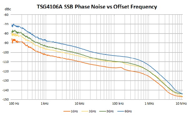
- SSB phase noise
- Output level is +5 dBm at 18 °C to 28 °C.
Carrier Offset from carrier, typical (dBc/Hz) 1 kHz 10 kHz 20 kHz 1 MHz 1 GHz -102 -110 -113 -124 2 GHz -96 -104 -107 -118 3 GHz -93 -102 -105 -120 6 GHz -87 -96 -99 -114
- SSB phase noise at 1 GHz carrier, maximum (output level +5 dBm, 5 ℃ to 40 ℃)
- 1 kHz offset
- –95 dBc/Hz
- 10 kHz offset
- –106 dBc/Hz
- 20 kHz offset
- –107 dBc/Hz
- 1 MHz offset
- –120 dBc/Hz
- 2 GHz offset
- –118 dBc/Hz
- >3 GHz offset
- –120 dBc/Hz


Phase setting (front panel outputs)
- Maximum phase step
- ±360º
- Phase resolution
- 0.01º (DC to 100 MHz)
0.1º (100 MHz to 1 GHz)
1.0º (1 GHz to 6 GHz)
OCXO time-base (Option M00 or Option E1)
- Oscillator type
- Oven-controlled, 3rd OT, SC-cut crystal
- Initial accuracy at calibration (20 minute warm-up, at 18 ºC to 28 ºC)
- <±0.02 ppm
- Temperature drift (0 ºC to 40 ºC)
- <±0.003 ppm
- Aging
- <±0.05 ppm/year
VCXO time base (Option M01)
- Initial accuracy at calibration (20 minute warm-up, at 18 ºC to 28 ºC)
- <±0.5 ppm
- Temperature drift (0 ºC to 40 ºC)
- <±5.0 ppm
- Aging
- <±3.0 ppm/year
Time-base input
- Frequency
- 10 MHz, ±2 ppm
- Amplitude
- 0.5 VP-P to 4 VP-P (–2 dBm to +16 dBm)
- Input impedance
- 50 Ω, AC coupled
Time-base output
- Frequency
- 10 MHz, sine
- Source
- 50 Ω, DC transformer coupled
- Amplitude
- >7.5 dBm
Internal modulation source
- Waveforms
- Sine, ramp, saw, square, pulse, noise
- Sine THD
- –74 dBc (typical at 20 kHz)
- Ramp linearity
- <0.05 % (1 kHz)
- Rate
- TSG4102A and TSG4104A
- 1 μHz to 500 kHz: < 62.5 MHz CF
1 μHz to 50 kHz: ≥62.5 MHz
- TSG4106A
- 1 μHz to 500 kHz: < 93.75 MHz CF
1 μHz to 50 kHz: ≥93.75 MHz
- Rate resolution
- 1 μHz
- Rate error
- 1:231 + time-base error
- Noise function
- White Gaussian noise (rms = dev / 5)
- Noise bandwidth
- 1 μHz < ENBW < 50 kHz
- Pulse generator period
- 1 μs to 10 s
- Pulse generator width
- 100 ns to 9999.9999 ms
- Pulse timing resolution
- 5 ns
- Pulse noise function
- Length 2N-1 PRBS 5 ≤ N ≤ 32, bit period 100 nS to 10 S
Analog modulation output
- Connector type
- BNC (rear panel)
- Impedance
- 50 Ω
- Function
- AM, FM, ΦM, Pulse
- Scale factor
- ±1 V for ± full deviation
- Pulse/Blank
- Low = 0 V
Hi = 3.3 V
External analog modulation input
- Connector type
- BNC (rear panel)
- Impedance
- 100 kΩ
- Function
- AM, FM, ΦM, Pulse
- Scale factor
- ±1 V for ± full deviation
- Pulse/Blank
- Low = 0 V
Hi = 3.3 V
- Input coupling
- DC or 4 Hz High-pass
- Pulse Threshold
- +1 VDC
- Input Offset
- < 500 μV
Amplitude modulation
- Range
- 0 to 100% (decreases above +7 dBm)
- Resolution
- 0.1%
- Modulation source
- Internal or external
- Modulation distortion, typical
- BNC output
- <1 % (fc < 62.5 MHz, fm = 1 kHz)
- N-type output
- <3 % (fc > 62.5 MHz, fm = 1 kHz)
- Modulation bandwidth (external)
- >100 kHz
Frequency modulation
- Minimum frequency deviation
- 0.01 Hz
- Maximum frequency deviation
- TSG4102A and TSG4104A
- Smaller of fc and 64 MHz – fc. In 0 to 62.5 MHz
Frequency range Maximum deviation 62.5 MHz < fc ≤ 126.5625 MHz 1 MHz 126.5625 MHz < fc ≤253.1250 MHz 2 MHz 253.1250 MHz < fc ≤ 506.25 MHz 4 MHz 506.25 MHz < fc ≤ 1.0125 GHz 8 MHz 1.0125 GHz < fc ≤ 2.0 GHz 16 MHz 2.025 GHz < fc ≤ 4.0 GHz (TSG4104A) 32 MHz - TSG4106A
- Smaller of fc and 96 MHz – fc. In 0 to 93.75 MHz
Frequency range Maximum deviation 93.75 MHz < fc ≤ 189.84375 MHz 1 MHz 189.84375 MHz < fc ≤ 379.6875 MHz 2 MHz 379.6875 MHz< fc ≤ 759.375 MHz 4 MHz 759.375 MHz < fc ≤ 1.51875 GHz 8 MHz 1.51875 GHz < fc ≤ 3.0375 GHz 16 MHz 3.0375 GHz < fc ≤ 6.0 GHz 32 MHz
- Deviation resolution
- 0.1 Hz
- Deviation accuracy, typical
- TSG4102A and TSG4104A
- < 0.1% of selected deviation + 5 Hz (fc < 62.5 MHz)
< 2% of selected deviation + 20 Hz (fc > 62.5 MHz)
- TSG4106A
- < 0.1% of selected deviation + 5 Hz (fc < 93.75 MHz)
< 2% of selected deviation + 20 Hz (fc > 93.75 MHz)
- Modulation source
- Internal or external
- Modulation distortion, typical
- < -60 dB (fc=100 MHz, fm=1 KHz, fd= 3 KHz)
- External FM carrier offset, typical
- < ±0.001 X FM deviation
- Modulation bandwidth, typical
- TSG4102A and TSG4104A
- 500 kHz (fc < 62.5 MHz)
100 kHz (fc > 62.5 MHz)
- TSG4106A
- 500 kHz (fc < 93.75 MHz)
100 kHz (fc > 93.75 MHz)
Phase modulation
- Deviation
- 0º to 360º
- Deviation resolution, typical
- 0.01º (DC to 100 MHz)
0.1º (100 MHz to 1 GHz)
1º (1 GHz and above)
- Deviation accuracy, typical
- TSG4102A and TSG4104A
- 2% (fc < 62.5 MHz)
3% (fc > 62.5 MHz)
- TSG4106A
- 2% (fc < 93.75 MHz)
3% (fc > 93.75 MHz)
- Modulation source
- Internal or external
- Modulation distortion, typical
- < -60 dB (fc = 100 MHz, fm =1 kHz, ΦD = 50º)
- Modulation bandwidth, typical
- TSG4102A and TSG4104A
- 500 kHz (fc < 62.5 MHz)
100 kHz (fc > 62.5 MHz)
- TSG4106A
- 500 kHz (fc < 93.75 MHz)
100 kHz (fc > 93.75 MHz)
Pulse modulation
- Pulse mode
- Logic High turns RF output ON
- On-Off ratio, typical
- BNC output
- > 70 dB
- Type-N output
- > 57 dB (fc < 1.0 GHz)
> 40 dB (1.0 GHz ≤ fc < 4.0 GHz)
> 35 dB (4.0 GHz ≤ fc < 6.0 GHz)
- Pulse feed-through, typical
- 10% of carrier for 20 ns at turn on
- Turn On-Off delay
- 60 ns
- RF Rise-Fall time, typical
- 20 ns
- Modulation source
- Internal or external pulse
Interface connectors
- USB
- USB 2.0, host
- Ethernet (LAN)
- 10/100 Base-T.TCP/IP and DHCP default
- GPIB
- IEEE488.2
- RS-232
- 4800 to 115,200 baud, RTS/CTS flow
External I/Q modulation (Option EIQ)
- Carrier frequency range
- 400 MHz to 2.0 GHz (TSG4102A)
400 MHz to 4.0 GHz (TSG4104A)
400 MHz to 6.0 GHz (TSG4106A)
- I/Q inputs (rear panel)
- 50 Ω, ±0.5 V
- I/Q full scale input
- (I2 + Q2)1/2 = 0.5 V
- Modulation bandwidth
- max 400 MHz RF bandwidth
- I or Q input offset
- <500 μV
- Carrier suppression
- > -45 dBc for fc ≤ 3 GHz
> -40 dBc for 3 GHz < fc ≤ 5 GHz
> -35 dBc for fc > 5 GHz
- I and Q baseband modulation bandwidth (3 dB from fc)
- > 200 MHz (fc < 2.5 GHz, RF BW >400 MHz)
> 150 MHz (fc > 2.5 GHz, RF BW >300 MHz)
Dual baseband generator (Option VM00)
- Channels
- 2 (I and Q)
- DAC data format
- Dual 14-bit at 125 MS/s
- Reconstruction filter
- 10 MHz, 3rd order Bessel LPF
- Arbitrary symbol memory
- Up to 16 Mbits
- Symbol rate
- 1 Hz to 6 MHz (1 μHz resolution)
- Symbol length
- 1 to 9 bits (maps to constellation)
- Symbol mapping
- Default or user-defined constellation
- Symbol source (User-defined symbols, built-in PRBS generator, or settable pattern generator)
- PRBS length
- 2n – 1 (5 < n < 32; 31 to about 4.3 × 10⁹ symbols)
- Pattern generator
- 16 bits
- Digital filtering
- Filter type
- Raised Cosine, Root Raised Cosine, Gaussian, Rectangular, Linear, Sinc, linearized Gaussian, C4FM, customized FIR
- Filter length
- 24 symbols
- Noise impairments
- Additive noise
- White, Gaussian
- Level
- –70 dBc to –10 dBc
Basic vector modulation formats (Option VM00)
- Formats by bit
Constellation 1-bit 2-bit 3-bit 4-bit 5-bit 6-bit 8-bit ASK 2ASK 4ASK 8ASK 16ASK FSK BFSK 4FSK 8FSK 16FSK PSK BPSK QPSK 8PSK 16PSK QAM n/a 4QAM n/a 16QAM 32QAM 64QAM 256QAM CPM BCPM 4CPM 8CPM 16CPM VSB n/a n/a 8VSB 16VSB
- Others
- OQPSK, DQPSK, π/4DQPSK, 3π/8 8 PSK
Digital modulation applications (typical)
- Digital modulation applications options
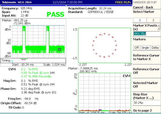
Option Application VM01 GSM VM02 GSM-EDGE VM03 W-CDMA VM04 APCO-25 Phase 1 VM05 DECT VM06 NADC VM07 PDC VM08 TETRA VM10 Audio clip (analog AM and FM) Option VM01 GSM, (GMSK, 270.833 kS/s, 935 MHz, 0 dBm), RMS EVM: 0.6%

Option VM02 GSM-EDGE, (3π/8 8PSK, 270.833 kS/s, 935 MHz, 0 dBm), RMS EVM: 0.30%

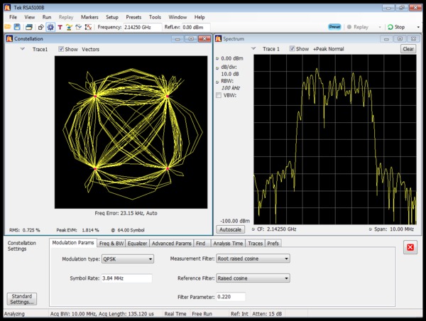
Option VM03 W-CDMA, (QPSK,3.840Mcps, 2.1425GHz, 0dBm), RMS EVM: 1.7%


Option VM03 W-CDMA (QPSK,3.840Mcps, 1.85 GHz, 0dBm), RMS EVM: 1.7%


Option VM04 APCO-25, (4FSK-C4FM, 4.8 kS/s,850 MHz, 0 dBm), Freq Err: 0.5%

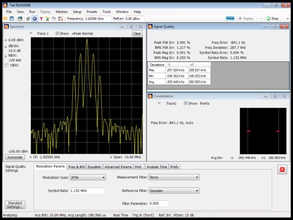
Option VM05 DECT, (2FSK 1.152 Mbps,1.925 GHz, 0 dBm), RMS FSK Err: 1.5%

Option VM06 NADC, (π/4 DQPSK, 24.3 kS/s, 875 MHz, 0 dBm), RMS EVM: 0.3%

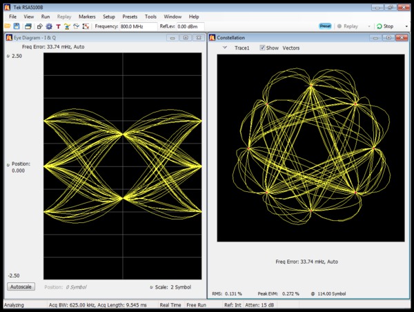
Option VM07 PDC, (π/4 DQPSK, 21 kS/s, 800 MHz, 0 dBm), RMS EVM: 0.6%

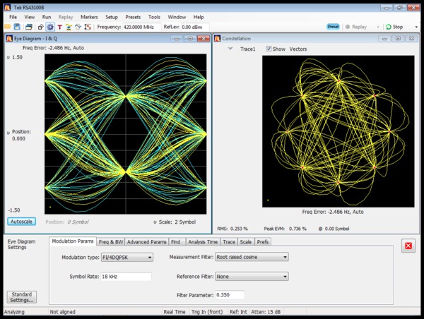
Option VM08 TETRA, (π/4 DQPSK,18 kS/s, 420 MHz, 0 dBm), RMS EVM: 0.7%

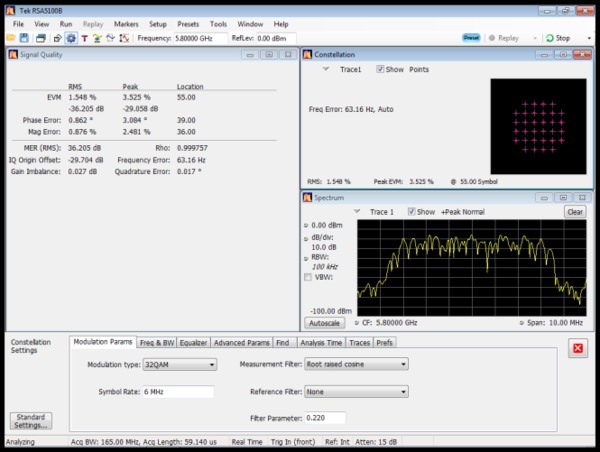
32QAM, (6 MS/s, 5.8 GHz, Root raised cosine filter, 0 dBm), RMS EVM: 1.6%

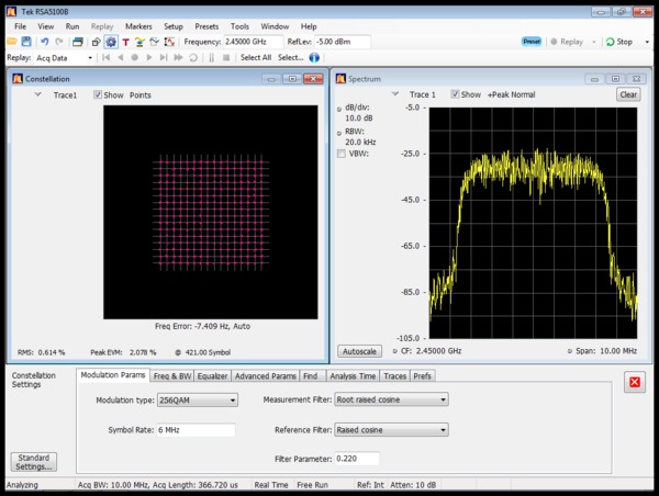
256QAM, (6 MS/s, 2.45 GHz, Root raised cosine filter, 0 dBm), RMS EVM: 1.1%

TSG4100A-ATT Option
- Nominal impedance
- 50 Ω
- Nominal attenuation
- 30 dB
- Frequency range
- DC to 6 GHz
- Attenuation deviation
- ±0.75 dB (DC to 6 GHz)
- Maximum VSWR
- 1.15 (DC to 4 GHz)
1.2 (4 GHz to 6 GHz)
- Power rating
- 5 Watt average power up to 25 ˚C ambient temperature, linearly derated to 1 Watt at 125 ˚C ambient temperature.
- Weight
- 0.052 kg
- Operating temperature
- -65 °C to 125 °C
- Compliance
- 2011/65/EU (RoHS) compliant
Rear-panel markers
- Type
- Symbol Clock, Data Frame, TDMA, and user-defined
- Amplitude
- 0.5 to 4 Vpp (–2 dBm to +16 dBm)
- Output impedance
- 50 Ω, AC coupled
Physical characteristics
- Dimensions
- Height
- 114 mm (4.5 in)
- Width
- 216 mm (8.5 in)
- Depth
- 347 mm (13.7 in)
- Weight
- 5.4 kg (12 lbs)
Operating characteristics
- Temperature
- Operating
- +5 °C to +40 °C
- Non-operating
- -20 °C to +60 °C
- Humidity
Operating Non-operating 5% to 95% relative humidity (%RH) at up to +30 °C 5% to 95% RH (Relative Humidity) at up to +30 °C 5% to 45% RH above +30 °C up to +40 °C, non-condensing 5% to 45% RH above +30 °C up to +40 °C, non-condensing
- Altitude
- Operating
- Up to 3,000 m
- Non-operating
- Up to 12,000 m
- Line power
- <90 W, 90 to 264 VAC, 47 to 63 Hz with PFC
- Vibration and shock
- Random vibration
Operating Non-operating 0.27 GRMS, 5 500 Hz, 10 minutes per axis, 3 axes (30 minutes total for Option M01) 2.28 GRMS, 5 500 Hz, 10 minutes per axis, 3 axes (30 minutes total for Option M01) 0.22 GRMS, 5 500 Hz, 10 minutes per axis, 3 axes (30 minutes total for Options M00 or E1) 2.13 GRMS, 5 500 Hz, 10 minutes per axis, 3 axes (30 minutes total for Options M00 or E1) - Mechanical shock
Non-operating Half-sine mechanical shocks, 50 g peak amplitude, 11 msec duration, 3 drops in each direction of each axis (18 total for Option M01) Half-sine mechanical shocks, 30 g peak amplitude, 11 msec duration, 3 drops in each direction of each axis (18 total for Options M00 or E1)
Regulatory information
- EC Declaration of Conformity - EMC
- EMC Directive 2004/108/EC
- EN 61326-1
- Radiated and Conducted emissions
- Class A
- Australia/New Zealand
- Australia Radio Communications Act 1992
- Korea
- KCC
- Safety
- Third Party Certification Standards
- UL 61010; CSA C22.2 No. 61010-1
- EC Declaration of Conformity - Low Voltage
- Low Voltage Directive 2006/95/EC; EN61010-1
- Safety Certification Compliance
Equipment type: Test and measuring Safety class: Class 1 - grounded product Pollution degree: 2 (as defined in IEC61010-1) Rated for indoor use only.
Ordering information
Use the following information to choose accessories and options for your probes.
Models
- TSG4102A
- Analog signal generator with 2 GHz frequency coverage, basic model
- TSG4104A
- Analog signal generator with 4 GHz frequency coverage, basic model
- TSG4106A
- Analog signal generator with 6 GHz frequency coverage, basic model
| Accessory | Description |
|---|---|
| RF cable | 1 meter, N-type to N-type RF cable |
| Documentation CD | All instrument models ship with a CD containing PDF files of user manuals in all available languages. |
| Installation and Safety Instructions | All instrument models ship with a printed Installation and Safety Instructions manual (multi-language: English and Russian). |
| Calibration | Statement of Calibration |
| Power cord | Country specific (see Power cord options) |
Warranty
Instrument options
Hardware options (All regions except North America)
Options M00 or M01 must be specified at the time of instrument order.
- M00
- Instrument with oven-controlled crystal oscillator (OCXO)
- M01
- Instrument with voltage-controlled crystal oscillator (VCXO)
- GPIB
- Adds GPIB interface
Hardware options (North America only)
Option E1 must be specified at the time of instrument order.
- E1
- Instrument with oven-controlled crystal oscillator (OCXO) time-base and GPIB interface
Hardware options (All regions)
- TSG4100A-RM1
- Single rack mount kit (can be ordered separately)
- TSG4100A-RM2
- Dual rack mount kit (can be ordered separately)
- TSG4100A-ATT
- 30 dB, 5 W RF attenuator up to 6 GHz
- D1
- A list of performance verification test results
Software options
To upgrade to vector/digital modulation capability and/or add more modulation options after initial purchase, order "TSG4100A-UP + VM xx” instead of “TSG410xA VMxx”.
- VM00
- Basic vector modulation package with internal 6 MHz modulation bandwidth
- VM01
- GSM modulation (requires Option VM00)
- VM02
- GSM EDGE modulation (requires Option VM00)
- VM03
- W-CDMA modulation (requires Option VM00)
- VM04
- APCO-25 modulation (requires Option VM00)
- VM05
- DECT modulation (requires Option VM00)
- VM06
- NADC modulation (requires Option VM00)
- VM07
- PDC modulation (requires Option VM00)
- VM08
- TETRA modulation (requires Option VM00)
- VM10
- Audio Clip (analog AM and FM)
- EIQ
- External 200 MHz modulation bandwidth (requires Option VM00)
Power plug options
- Opt. A0
- North America power plug (115 V, 60 Hz)
- Opt. A1
- Universal Euro power plug (220 V, 50 Hz)
- Opt. A2
- United Kingdom power plug (240 V, 50 Hz)
- Opt. A3
- Australia power plug (240 V, 50 Hz)
- Opt. A5
- Switzerland power plug (220 V, 50 Hz)
- Opt. A6
- Japan power plug (100 V, 50/60 Hz)
- Opt. A10
- China power plug (50 Hz)
- Opt. A11
- India power plug (50 Hz)
- Opt. A12
- Brazil power plug (60 Hz)
- Opt. A99
- No power cord
Language options
Request the option below if you would like to order a printed verison of the English User Manual. (An electronic version of this manual is provided as a PDF on the CD that shipped with your instrument and is also available for download from the Tektronix Web site.)
- Opt. L0
- English manual
Service options
- Opt. C3
- Calibration Service 3 Years
- Opt. C5
- Calibration Service 5 Years
- Opt. D1
- Calibration Data Report
- Opt. D3
- Calibration Data Report 3 Years (with Opt. C3)
- Opt. D5
- Calibration Data Report 5 Years (with Opt. C5)
- Opt. R5
- Repair Service 5 Years (including warranty)


