Introduction
Increasing data rates have resulted in the requirement for post processing of data before measurements can be taken. This post processing typically involves de-embedding measurement circuits, embedding compliance channels, and applying equalization to open closed eyes. During the simulation process, S-parameters and IBIS-AMI models are often used in system analysis to model silicon specific behavior, while measurement equipment has traditionally used S-parameters and reference equalization models. It is often desired to correlate the results from the live acquisition with simulations.
Until recently, IBIS-AMI model processing has not been available on measurement equipment. S-parameter modeling and IBIS-AMI support on a real-time oscilloscope allows the de-embedding of the measurement circuit and embedding of the simulation circuit in real-time enabling evaluation of true system performance. Measurements can then be performed on the waveform after the IBIS-AMI receiver model has been applied and compared with simulation results. The availability of IBIS-AMI modeling on measurement equipment allows for the same models to be run in the measurement and simulation environments.
This paper will cover an introduction to S-parameter modeling and IBIS-AMI models in measurement systems and end with correlation results based on using S-parameters and IBIS-AMI models in measurement and simulation environments on a SAS 12Gb/s signal, in addition to comparisons of using a reference equalizer in the measurement system.
IBIS-AMI Introduction
The IBIS Algorithmic Modeling Interface (IBIS-AMI) is a behavioral model standard defined in IBIS 5.0 specification created by the IBIS Open Forum and approved by the members in 2008. An IBIS-AMI model is a behavioral model written in a high level programming language that can be run on several different simulators that support the IBIS-AMI standard. They are created to be functionally the same as a Spice model but enable faster simulations similar to the IBIS model. IP is protected because the model is compiled for the operating system it is simulated on.
IBIS-AMI models work in both the statistical and the time domain by using an impulse response or a time domain waveform as input to the model. The output of the model is either an impulse response or a time domain waveform after the equalization has been applied. Further details in this paper are based on the time-domain waveform approach, also known as bit-by-bit analysis.
S-parameter modeling in measurement systems background [1]
High frequency design engineers commonly use scattering parameters (S-parameters) to mathematically model RF and microwave multi-port networks. Since many analysis solutions represent model blocks with S-parameters it is important to have a good understanding of how they are defined, how they are measured, and how they are used and interpreted.
Converting S-parameters to the Time Domain
The time domain is another useful view for analyzing the S-parameter data for correctness or to troubleshoot problems that can occur. The IFFT can be used to make this conversion; however, several mathematical steps must be performed before the IFFT function can be applied.
The procedure for converting the S-parameter to the time domain is as follows:
- Extrapolate the S-parameter from the start frequency point back to DC. Since Sparameters are commonly obtained from a VNA measurement, the data set will not contain DC unless it was measured independently and added to the file.
- Extrapolate or truncate to set the stop frequency to the Nyquist point at ½ the sample rate.
- Create the data set for frequencies from Nyquist to the sample rate by copying the complex conjugate of the data from the first point after DC to Nyquist in reverse order.
- Compute the IFFT of the resulting S-parameter data. If this step is performed correctly then the IFFT of the S-parameter data will result in time domain data that is real only, with the imaginary part equal to zero.
Cascading S-parameters and aliasing
The cascading of blocks represented by S-parameters is a key operation in the serial data link simulation and analysis system. An example of a cascaded set of 4-port S-parameter blocks is shown in Figure 1. The circuit connections are defined by port numbers assignments. The S-parameter reference impedance for the ports that are connected must be the same in order for the cascaded results to be correct. This example shows the cascading of the transmitter package model, transmission line, receiver package model, and the receiver input impedance.

In order to compute transfer functions which represent different test points or virtual probing locations, it is necessary to combine several cascaded blocks into a single block. If the system delay of the cascaded blocks is greater than the time interval covered by the individual block S-parameters then aliasing will occur. In the time domain the aliasing results in pulse response features occurring in the wrong time position and they may be reversed in time order. This is the result of phase aliasing in the frequency domain where there are less than 2 samples per revolution.
To avoid aliasing, the individual S-parameters need to be re-sampled to provide smaller frequency spacing to cover the increased time interval for the combined S-parameters.This can be done by resampling multiple S-parameters that potentially have different frequency spacing and different bandwidth.
The process is described below:
- Extrapolate all S-parameters data to DC if the S-parameters don’t have a DC value. S-parameters measured from a VNA do not have a DC value. TDR measured S-parameters have a DC value.
- Determine the common maximum frequency for all of the S-parameter sets. This value can be the maximum frequency of all of the S-parameter sets in the cascade. Extrapolate each S-parameter set to beyond the maximum common frequency.
- Convert extrapolated frequency domain S-parameters to obtain the time domain impulse responses using an IFFT.
- Determine the actual common sample period between the impulse responses.The actual common sample period can be taken as the minimum of sample periods of the impulse responses. Then resample the impulse responses so they all have the same sample rate.
- Zero fill the impulse responses at proper positions to get increased time interval. The increased time interval can be determined as multiples of the sum of all the time intervals represented by each S-parameter.
- Convert time domain zero filled impulses to frequency domain using FFT.
- Truncate the lower frequency and high frequency points that are extrapolated. (This step is optional.)
- At this step all S-parameters have been resampled at the same frequency points with sufficient frequency resolution. For each frequency point, combine the S-parameters for each block to be cascaded.
Once the S-parameter data has been re-sampled, filters are created that represent selected probe points in the system.
Introduction to IBIS-AMI Modeling in Measurement Systems
In the past, measurement systems have relied on using reference equalization techniques for the receiver. These techniques were implemented to the requirements defined in specific standards. For example, PCI Express uses a CTLE + 1 Tap DFE as a reference equalizer with the optimization being done on eye area. SAS on the other hand, specifies a 3-tap DFE for 6Gb/s and 5-tap DFE for 12Gb/s and the optimization is done on RMS noise. Compliance testing requires the use of reference equalizers as it is assumed that the equalization techniques built in actual silicon are equal or better than the reference equalizer. This is sufficient for compliance testing, but when silicon specific behavior needs to be observed they fall short.
Implementing IBIS-AMI model support in a real-time oscilloscope presents new challenges that do not exist in simulation environments. Many IBIS-AMI models require an integer number of samples per unit interval. Since the number of samples per unit interval on a real-time scope is related to the sample rate and bit rate, it is not guaranteed that the waveform will have an integer number of samples per unit interval. This requires the re-sampling of the waveform to meet the number of samples per bit (i.e. 16, 32, 64, etc) that is required by the model. Once this re-sampling has taken place, the waveform can be processed using the IBIS-AMI model.
IBIS-AMI models have a parameter for ignore bits, which specifies the number of bits to ignore from the measurement. Ignore bits are at the beginning of the waveform and represent the settling time of the algorithm. AMI models also support block processing. Block processing mode of operation divides the interpolated waveform samples into segments specified by the Block Processing Size (entered in K samples). The AMI model Get_Wave function is consecutively called for each block. The resulting waveform samples are decimated to the sampling rate of the scope (if needed) and combined to produce a full output record. The AMI model can produce intermediate results at each call to Get_Wave. For example, it produces an adaptation record that shows the convergence of automatic gain control, equalization coefficients or other varying parameters.
An example of a IBIS-AMI configuration is shown in the figure below.

Correlation Study of Simulation vs. Measurement Systems
Validation of high speed designs often includes correlation between measurements taken on a live signal vs. simulation. These activities require the de-embedding the effects of the measurement circuit, for example PCB traces, probes, cables, and test fixtures, from the live waveform. Verification of de-embedding can be done by first removing the effects of the measurement circuit and then re-embedding those effects and comparing the resulting waveform with the acquired waveform. If the two waveforms match, a high degree of confidence can be assumed in the ability for the measurement circuit to be deembedded. Once the de-embedding has been verified, the simulation circuit can then be embedded. This consists of the transmitter output impedance, transmitter package model, transmission line, receiver package model, and receiver input impedance. In many cases, the effects of the simulation circuit result in a completely closed eye. Receiver equalization can then be applied to observe the signal as it would be seen at the slicer of the receiver inside of the silicon. Once these results are available from the live signal acquisition they can then be compared with simulation results.
System Configuration
The following topology outlines the measurement and simulation circuits that were used in this experiment. The experiment was done using both a long and short transmission line.
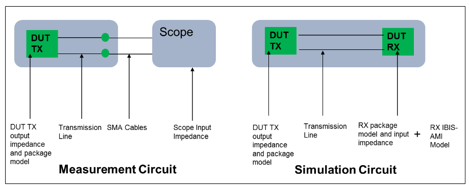
The measurement circuit represents the physical test setup and includes all the elements that are required to remove the effects of the measurement circuit in order to get back to the Thevenin equivalent voltage. The goal is to completely remove the effects of the measurement circuit so simulations can be done.
In the setup used for this experiment the measurement circuit consists of the output impedance of the transmitter, transmitter package model, the transmission line from the transmitter to SMA connectors, SMA cables, and the input impedance of the real-time oscilloscope. S-parameters were used to model each element of the measurement circuit. The S-parameter models for the transmitter output impedance and package model were extracted from a simulation environment and represent the nominal ideal condition without variation. The transmission line model was measured at room temperature out to 40 GHz with a VNA. The actual device is 12Gb/s SAS and all tests were done using a PRBS7 pattern.
The simulation circuit consists of the output impedance and package model of the transmitter, the transmission line, the package model and input impedance of the receiver, and the receiver equalization model. As with the measurement circuit, S-parameters models for the transmitter output impedance and package model were extracted from a simulation environment as were the models for the receiver package model and input impedance. The transmission line was measured at room temperature with a VNA. An IBIS-AMI model was used to model the equalization of the receiver.
When measuring a live device, the measurement circuit is first de-embedded and removed from the acquired waveform, the simulation circuit is embedded and the IBISAMI model is applied. In contrast, in the simulation environment, the measurement circuit does not exist. However, in some cases it may be desired to model the effects of the measurement circuit in the simulation environment. The S-parameters from the measurement circuit can be used in the simulation environment to model the loading effects on the circuit.
Validation of measurement circuit de-embedding
Before correlation between the measurements on the actual DUT and simulation can be done, it is desired to validate the effects of de-embedding the measurement circuit. One way to verify the effects is to acquire the live signal from the DUT, de-embed the measurement circuit and then embed the measurement circuit. The acquired waveform and the waveform after the embed process should be similar.
The first step is to configure the measurement circuit in the link analysis software on the real-time oscilloscope. This consists of configuring the transmitter output impedance of the physical device. In this example, a 2-port S-parameter model was used.

Next, the transmitter package model, transmission line, and scope input impedance are defined using 4-port S-parameter models and two 1-port models for the input impedance of the scope. These elements must be cascaded together to provide an accurate deembed. The details of this process were covered previously in the Cascading Sparameters and aliasing section.

The desired goal is to observe the output of the transmitter driving into an ideal 50Ω load. This is done by configuring the simulation circuit with the output impedance of the transmitter; which is the same as in the measurement circuit. The transmitter package model, transmission line model and scope input impedance represent the remainder of the simulation circuit.
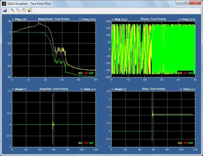
The desired observation point in this case is the output of the transmitter, which is represented by test point Tp2 in the figure below.

When de-embedding it is important to consider the signal to noise ratio of the acquired signal and tune the bandwidth accordingly. A bandwidth filter can reduce the gain of noise by filtering out the high frequency components. Further control of the pass band, transition band, and stop band responses provide the ability to control noise attenuation, rise time, preshoot, and overshoot. By default many link analysis solutions will automatically pick a bandwidth cut-off limit, for example by choosing the frequency that cross a specific dB point (i.e. -14dB).
In this example, it was necessary to raise the bandwidth limit in order to extend the frequency content of the de-embedded signal. When using auto, the frequency cut-off was set to 15 GHz and this was increased to 20 GHz for more accurate results. The result is a transfer function at Tp2 with the profile in Figure 7. The gain in frequency seen at around 16 GHz is due to the channel model.
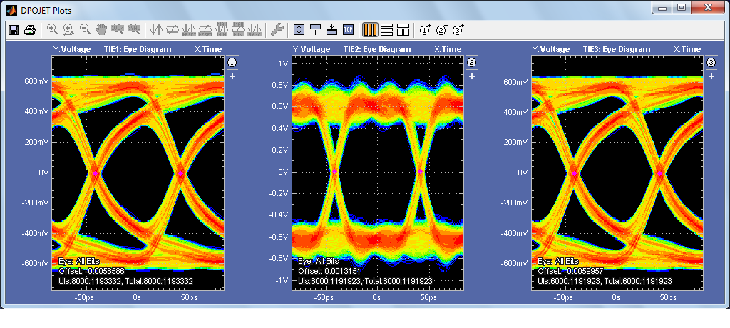
Once the transfer function has been created it can be applied to the acquired waveform. The results below show the eye diagrams for the acquired waveform, the waveform at Tp2 (before the channel) and the waveform at Tp3 (after the channel). The acquired waveform and the waveform at Tp3 should match as is illustrated in the example below.
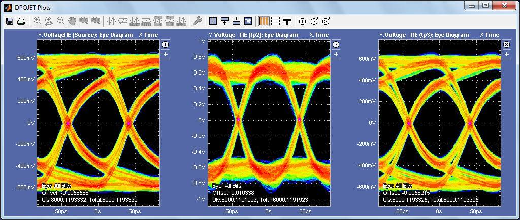
In contrast, as described above lowering the bandwidth limit will have the consequence of filtering out the higher frequency content of the signal. While the lower frequency content follows a similar shape to the acquired signal, the high frequency content as seen in the eye diagram below has more of a sine wave appearance and does not provide a close match as seen when the bandwidth limit is extended to 20GHz.
Now that confidence has been built in the de-embedding procedure the next step is to compare the simulation with the measurement results.
Simulation and Measurement Results Correlation
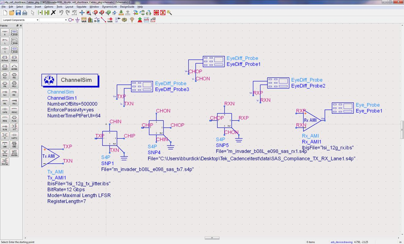
The simulation environment was configured to represent the transmitter by simulating at 12Gb/s PRBS7 and an IBIS-AMI transmitter model. The transmitter output parameters are represented as follows:
- PVT = Typical Process, 0.9V, 25C
- TxSwing = 15 (0 -15 range) (600mV peak)
- CMain = 21 (0 – 21 range)
- CPost = 0 (0 – 17 range)
- CPre1 = 0 (0 – 7 range)
- CPre2 = 0 (0 – 3 typically 0)
The transmitter output impedance and package model are represented by the same Sparameter models used in the measurement environment. Additional S-parameter models represent the transmission line, receiver package and input impedance. The receiver equalization is modeled using IBIS-AMI.
The correlation was done on three different configurations:
- No transmitter equalization with a short channel
- No transmitter equalization with a long channel
- Transmitter equalization with a long channel
The simulation setup is shown in Figure 10.
No transmitter equalization with a short channel
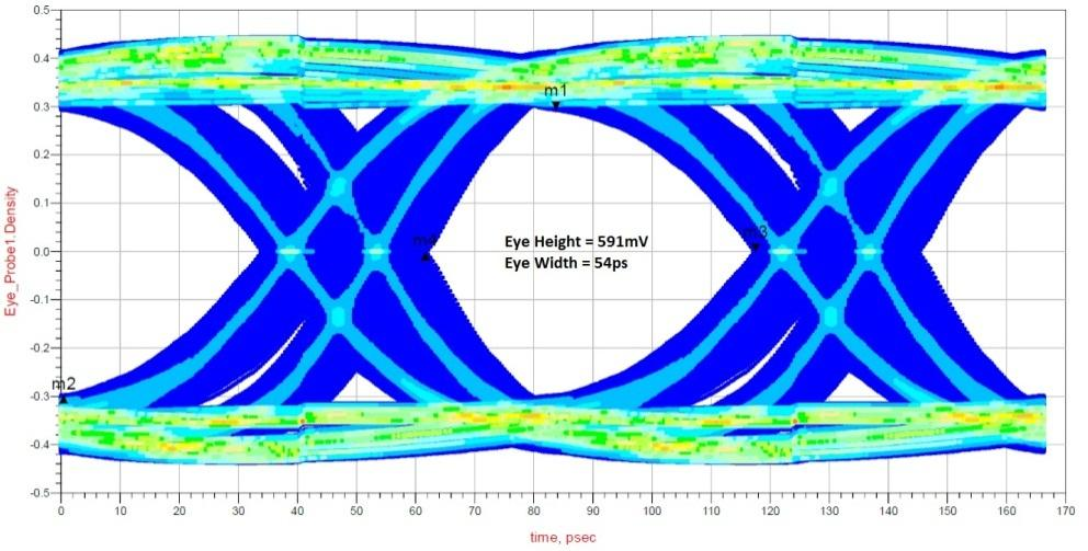
When simulating the transmitter with no equalization and using a short channel, the result of the simulation is shown below.
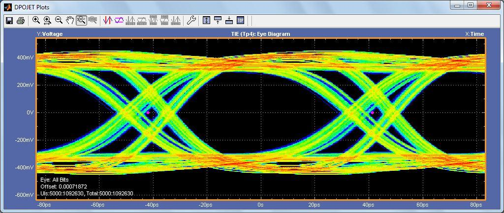
In contrast, the measurement results are shown below. Note the shape of the eye diagram vs the simulation results. The results correlate quite well, within 5% for eye height and eye width.
No Transmitter equalization with a long channel
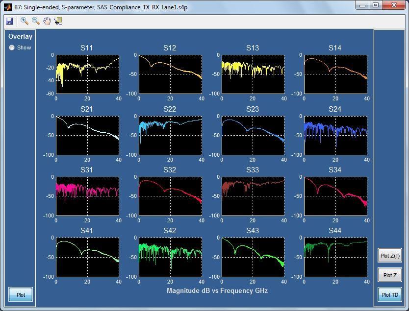
A more interesting case is to look at the same setup, but change the channel to a longer channel. The S-parameter model of the channel is shown in Figure 13. Unlike the short channel, a closed eye is expected at the far end of this channel.
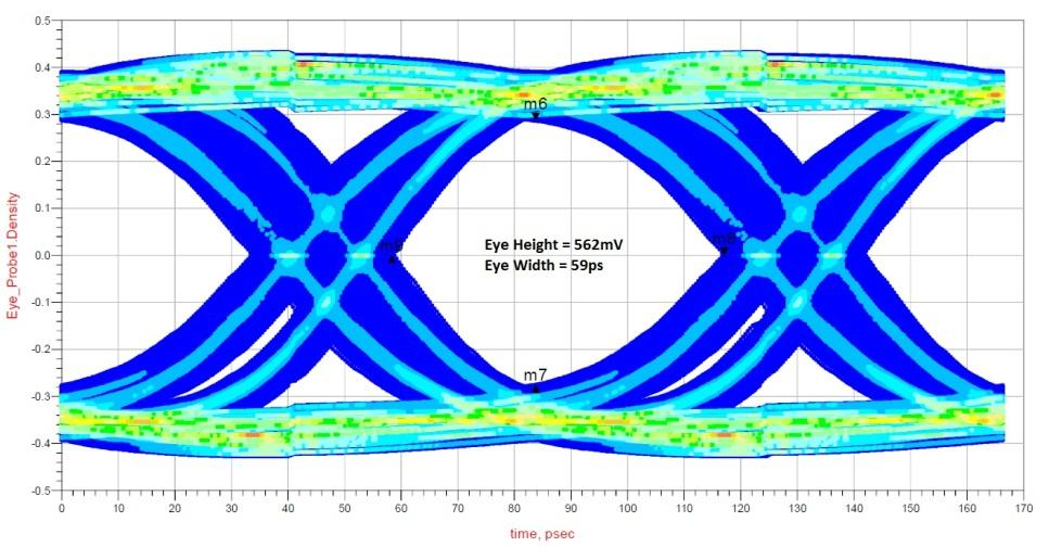
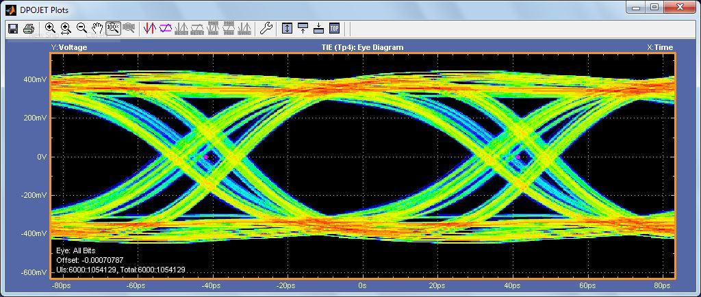
The results of the simulation vs. measurement are shown in Figures 14 and 15. Again very good correlation within 5% is seen on the eye height and eye width measurements.
Transmitter equalization with a long channel
In the final setup, the transmitter settings were set to:
- PVT = Typical Process, 0.9V, 25C
- TxSwing = 15 (0 -15 range) (600mV peak)
- CMain = 21 (0 – 21 range)
- CPost = 7 (0 – 17 range)
- CPre1 = 4 (0 – 7 range)
- CPre2 = 0 (0 – 3 typically 0)
Again, the results between simulation and correlation are very similar.
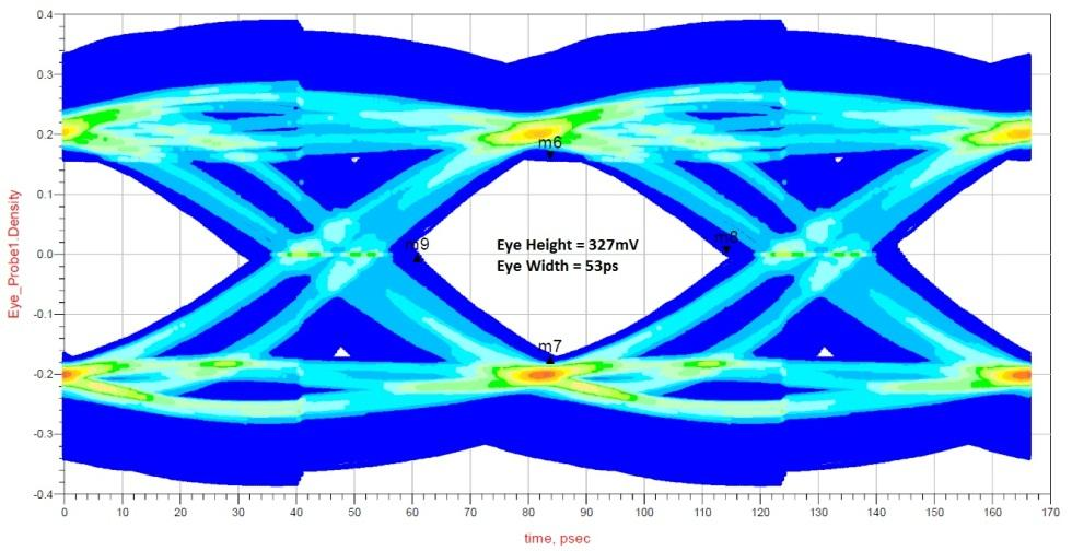
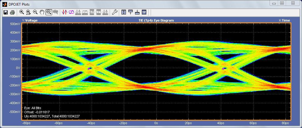
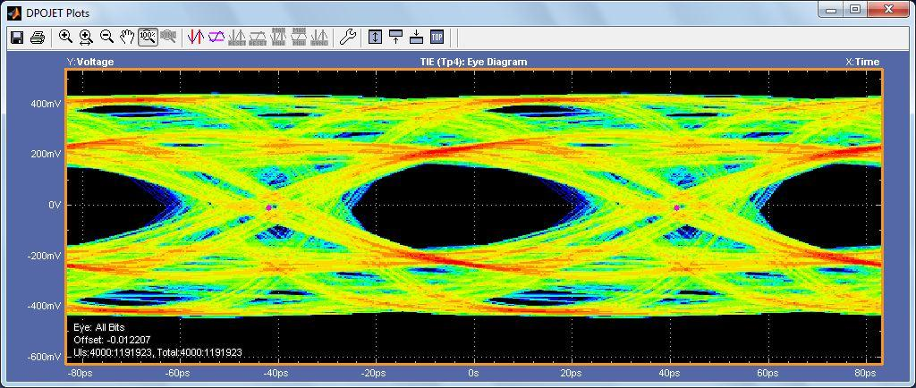
In all three examples, the measurement environment was setup to ensure that the ignore bits were not being measured. This is critical to ensure that the resulting measurements do not include the time before the receiver coefficients have settled. Figure 17 shows the results with the ignore bits vs. Figure 18 that does not have the ignore bits removed. While the overall measurement results are similar, the shape of the eye diagram is dramatically different.
Comparison of reference equalizers vs. silicon specific IBIS-AMI models
The last part of the analysis was to compare the results of using reference equalizers vs. silicon specific IBIS-AMI models. Reference equalization models are built into many link analysis solutions and are commonly used for compliance testing. In this case, the DFE model used in the measurement environment is based on SAS and is designed to minimize RMS noise. Reference equalizers can fall short in modeling actual DUT behavior as shown in the examples below. The comparison between reference equalizers and IBIS-AMI models was done across all three examples with similar results. A comparison will be shown for the example with transmitter equalization enabled and a long channel.
Figure 17 above represents the output of the IBIS-AMI model and Figure 19 below represents the output of the SAS compliance DFE. Since the IBIS-AMI model uses a 10-tap DFE the reference DFE was also setup to 10-taps.
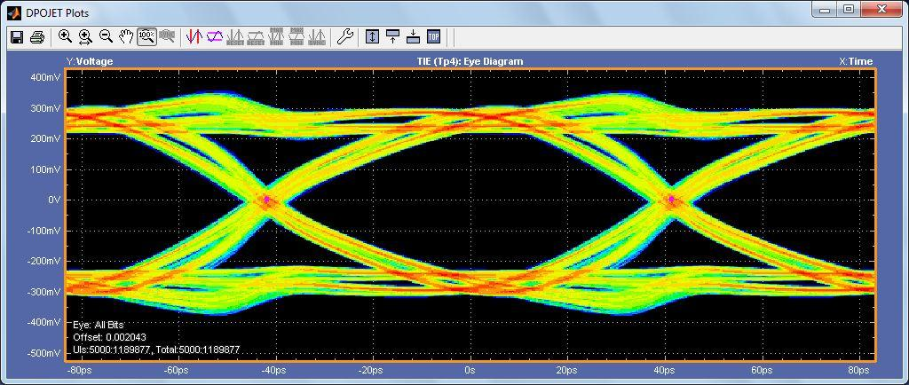
As shown, the results between the two vary to a large degree. This is seen in both the shape of the resulting eye diagram and the measurement results. The reference equalizer is an ideal mathematical model that can implement the DFE as defined in the standards. The reference equalizer does not take into account several limitations specific to the implementation in silicon, for example: exact discrete-time and digital clock recovery function, automatic gain control, and/or DFE coefficient limitations. The IBISAMI model is designed using the architecture of the actual receiver and has impairments to mimic the silicon such as jitter, voltage variation, temperature variation, and bandwidth limitations.
Conclusion
Based on the results from this analysis, it is shown that good correlation can be met between the simulation and measurement environments. It is critical that good Sparameter models are available to represent the transmitter, transmission line, and the receiver. Understanding how these models will be created and used at design time is important. Furthermore, while reference equalization models work well for compliance testing in the cases where true silicon behavior needs to be observed, IBIS-AMI models can be used to provide a true representation of the signal.

