Introduction
Crystalline materials are fundamental to modern electronics and optoelectronics. Therefore, the electrical properties of these materials, such as their (anisotropic) conductivity and photoconductivity, as well as the temperature dependencies associated with these properties, are of great interest to researchers. The crystals grown using a number of crystallization techniques may be small in size and often exhibit very high resistances. This application note describes how to measure resistances as high as 1017Ω in a specially designed measurement chamber, as well as in a Molecular Beam Deposition (MBD) system that allows making in-situ measurements during crystal or film growth.
Test Description
High resistances (up to 1017Ω) are usually measured by applying a constant voltage, then measuring the resulting current. In general, using a higher voltage allows making a more accurate measurement. However, the level of voltage that can be applied to small crystals (those <1mm in size) is limited by the electrical breakdown of air between the contacting electrodes at an electrical field of 1kV/mm.
There are two ways to measure these crystals at higher voltages. The first technique is to measure under high vacuum conditions, which requires a pressure level lower than 10–4 mbar. The second approach is to use an inert gas with a higher breakdown threshold (such as SF6) under a slight overpressure (1-2 bar). The advantage of using high vacuum is that there’s virtually no breakdown limit. However, when using an inert gas, it’s much easier to control the temperature of the sample than when measuring in high vacuum, where no gas is available to transfer heat.
Test System Configurations
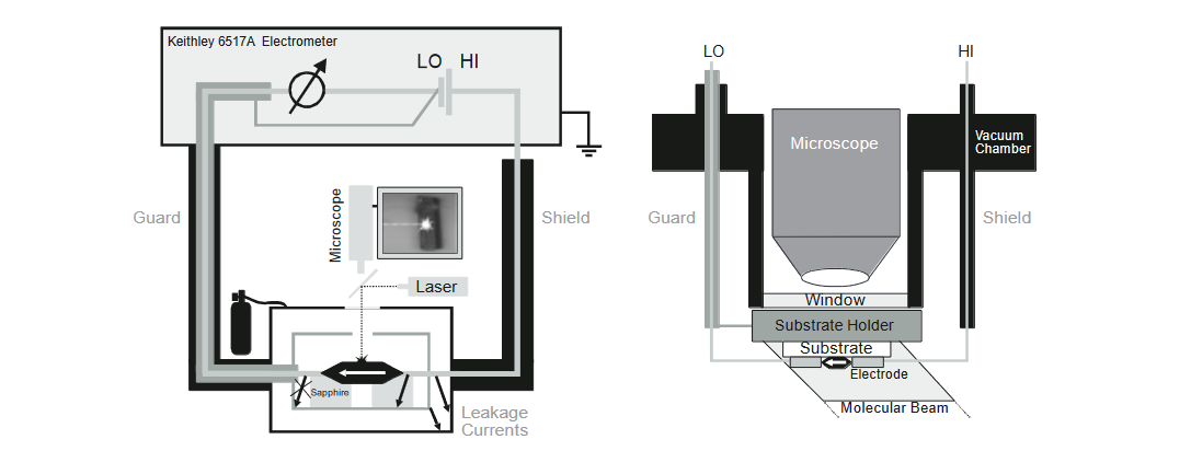
We chose to use the Model 6517A Electrometer/High Resistance System as the measurement instrumentation for these test configurations because it offers femtoamp-level sensitivity and has an integrated programmable 1000V source. Low noise triax cables connect the electrometer with the measurement chamber (which is filled with inert gas) or the MBD ultra high vacuum system. Both setups have windows for illuminating the sample with a laser beam to measure photoconductivity and for visual monitoring of the measurement process via a microscope. The temperature can be adjusted from –20°C to 120°C. The setup is illustrated in Figure 1.

Methods and Techniques
Contacts
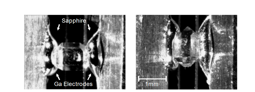
Measuring the anisotropic properties of crystals often requires making contact with the same crystal in multiple directions, e.g., parallel and perpendicular to a crystal axis. Therefore,researchers need a material that provides reliable electrical contact, but which can be removed after the measurement is made without leaving contaminants behind on the sample. Typical adhesive materials that “stick well” or contain solvents like conductive silver or carbon are unsuitable. Gallium, a metal with a low melting point of 30°C, provided good results when its melting point was lowered to 20°C by adding 8% tin. Gallium’s high surface tension means it doesn’t wet most materials, so it’s easy to remove after the measurement is made. As Figure 2 shows, contact with the extremely small crystal samples (down to 100µm) was made with drops of liquid gallium placed on the electrodes in the test fixture. A microscope was used to visualize the contact area and guide the positioning of the gallium drops.

Sample Mounting
When characterizing small samples, the substrate on which the sample is mounted can become a significant source of measurement error, as result of both its volume and surface resistivity. The obvious way to prevent any leakage current through a (possibly contaminated) substrate surface is to use two insulator plates separated by a gap, rather than placing the sample on a single plate. To simplify testing small samples of various sizes, the mounting hardware should include a micrometer screw to adjust the width of this gap.
Typical Sources of Error
Shielding and Guarding
To reduce electrostatic interference, surround the sample and the cables with a conductor at ground potential (shield).
To prevent leakage currents from affecting the measurements, surround the connection to the electrometer input by a conductor at the same potential (guard). For measuring currents, this is done by connecting the guard to the LO terminal of the voltage source.
In a high vacuum system, the vacuum chamber, which is commonly grounded, acts as the shield. The sample holder should be connected to guard potential to prevent leakage currents. Low noise measurements (1fAp-p) can be made as long as the signal cabling inside the chamber (e.g., heating elements) is shielded with a grounded conductor and the pumps (e.g., turbomolecular pumps) are covered with a grid. For applications that require ultra-high vacuum, use Teflon® wires because they outgas very little. If a triax feedthrough isn’t available, use an insulated coaxial feedthrough (e.g., BNC) in conjunction with an additional shielding cylinder that connects the outer shield of the cable with the vacuum chamber.
Temperature Stability
Temperature changes in the measurement system cause thermal expansions and, therefore, changing capacitances, introducing additional noise in the current. If measurements are performed at ambient temperature without additional heating or cooling, the system temperature is usually sufficiently stable during measurement. However, if temperature-dependent measurements are necessary, the temperature stability should be better than 0.1K.
To measure photoconductivity, it’s essential to minimize heating of the sample and measurement system due to light absorption. This requires using materials with good heat conductivity. For this application, the best choice is to use a sapphire substrate and copper electrodes to mount the sample, as shown in Figure 2. In addition to its excellent volume resistivity and a surface with good resistance to water absorption, sapphire has good thermal conductivity and doesn’t absorb light over a wide spectral range. To minimize the amount of heat the system absorbs, exercise care to illuminate only the sample (e.g., by focusing the light or using a laser beam), not the surrounding electrodes and shields. System heating can cause a rise in current, much as it does in photoconductivity measurements.
In many crystals, electric dipoles are ordered in a preferred direction, resulting in a charged surface. During thermal expansion, the surface charges shift, which causes the pyroelectric effect, a current peak of the opposite polarity when the light shutter is opened (which increases temperature) and closed (which decreases temperature).
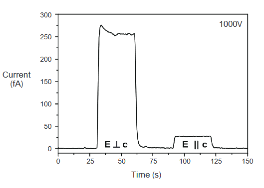
Avoid using Teflon substrates when measuring photoconductivity this material stores charges, which will also shift during thermal expansion, producing an effect similar to the pyroelectric effect. Figure 3 illustrates an experimental photoconductivity measurement technique.

Photoelectric Effect
At wavelengths shorter than a certain material-dependent wavelength, light is energetic enough to induce emission of electrons from the electrode material. This leads to an ionization of the gas between the electrodes, providing a conductive path. If the measurement is performed in high vacuum, these electrons produce an additional current. To avoid these effects, the wavelength chosen for illumination should be greater than the threshold for the photoelectric effect. For gallium, this wavelength is 295nm.
Stored Charges
Given that charges are stored in many insulators (especially Teflon), it may take hours for the current to reach equilibrium after changing the applied voltage or temperature, especially for samples with very high resistances and at high applied voltages. Don’t start the measurement until equilibrium is reached.
Equipment List
- Model 6517A Electrometer
- Low noise triax cable
- PC, IEEE cable, etc.
- SF6 gas bottle
- Gallium
- Custom-made measurement chamber with triax, high voltage feedthrough
Test System Safety
Accidental electrical shorts or breakdowns between the electrodes are likely when small samples are used. To prevent excessive currents, place a protection resistance in the circuit to limit the current to 1mA or less.
Many electrical test systems or instruments are capable of measuring or sourcing hazardous voltage and power levels. It is also possible, under single fault conditions (e.g., a programming error or an instrument failure), to output hazardous levels even when the system indicates no hazard is present.
These high voltages, power levels, and compressed gas usages makes it essential to protect operators from any of these hazards at all times. Protection methods include:
- Design test fixtures to prevent operator contact with any hazardous circuit.
- Make sure the device under test is fully enclosed to protect the operator from any flying debris.
- Double insulate all electrical connections that an operator could touch. Double insulation ensures the operator is still protected, even if one insulation layer fails.
- Use high reliability, fail-safe interlock switches to disconnect power sources when a test fixture cover is opened.
- Where possible, use automated handlers so operators do not require access to the inside of the test fixture or have a need to open guards.
- Provide proper training to all users of the system so they understand all potential hazards and know how to protect themselves from injury.
- Observing the usual safety precautions for compressed gases (SF6). Some gases used are not necessarily toxic, but can be heavier than air, thus displacing oxygen and creating a breathing safety hazard.
- Gallium is irritating to the eyes, respiratory system, and skin, so avoid exposure when working with it by using protective eyewear, gloves, clothing, and an appropriate respirator.
It is the responsibility of the test system designers, integrators, and installers to make sure operator and maintenance personnel protection is in place and effective.
Conclusions
Current measurements at low noise levels (1fAp-p without filtering) can be performed at a maximum of 1000V with a Keithley 6517A Electrometer. By using a carefully designed measurement chamber and good quality insulators, leakage currents can be completely avoided, which allows measuring resistances up to 1017Ω accurately. This measurement capability can be maintained during temperature dependent or photoconductivity measurements if the temperature stability is better than 0.1K. Electrical breakdown of air between the electrodes at high voltages can be suppressed using an SF6 atmosphere or high vacuum. If cables and pumps inside a Molecular Beam Deposition high vacuum system are shielded, current measurements can be done in-situ during thin film growth with the same sensitivity, which is especially useful for materials with low conductivity like organic molecules.

