Timing Jitter Analysis and Evaluation
Timing jitter (or simply "jitter") is an undesirable phenomenon inherent to any electrical system that represents timing information with voltage transitions. Traditionally, relatively slow signal rates were adopted in electrical systems to mitigate the adverse effects of timing jitter. As a result, errors induced by jitter were small compared to the time intervals damaged by these errors. Today, the timing margins associated with high-speed serial buses and data links indicate a need for stricter jitter control in system design.
As signal rates rise to 2GHz and voltage amplitudes are reduced for power savings, timing jitter in systems now occupies a significant portion of the signal interval. In such environments, jitter becomes a limiting factor in basic performance. Understanding what jitter is and how to evaluate it is the first step in successfully adopting high-speed systems that meet performance requirements with high reliability.
A detailed definition will be covered in Chapter 2, but theoretically, jitter is the deviation from the "correct" position of a timing edge. In timing-based systems, timing jitter is the most straightforward and direct form of non-ideal behavior. Since jitter is a type of noise, it must be treated as a random process and statistically evaluated.
Having a statistical method to measure jitter allows components and systems to be compared against each other and against chosen limits. However, this alone is insufficient for efficiently improving and debugging modern designs. Only by fully analyzing jitter can the root causes be identified and systematically reduced, rather than through trial and error. This analysis allows for the visualization and analysis of jitter, which will be explained in Chapters 3 and 4.
Although there are many similarities in the causes, behavior, and evaluation of electrical and optical jitter, the equipment used for measuring jitter in optical systems differs from that used in electrical systems. This book primarily discusses jitter in electrical systems.
Chapter 1: Problems Caused by Jitter
“It costs nothing to guess, but guessing wrong can be costly” — Chinese proverb
Why is it necessary to consider jitter? How does jitter affect system performance? This chapter examines the impact of jitter in two cases: high-speed computer buses and serial data links. The effects of jitter in each case will be discussed in detail.
Computer Bus Design
For example, suppose you are designing a new embedded processor and occasionally encounter data errors when reading flash memory. The design engineer suspects that the address decode generating the flash memory CE (chip enable) does not meet the necessary setup time relative to the WE (write enable) rising edge. By probing the CE and WE signals with a high-speed oscilloscope, you observe their timing relationship. After ten single-shot acquisitions, you measure times between 87-92ns, all comfortably above the minimum setup time of 75ns. But what is the appropriate margin? Are these times sufficient to dispel concerns about violating the required setup time? What percentage of the time do violations occur?
By overlaying millions of waveforms in infinite persistence mode and observing a setup time as short as 82ns, you conclude that it might be a setup time issue. However, could this problem be due to clock period variations, the address decoder, or another violation elsewhere in the system?
Serial Data Links
Suppose the development deadline for a Gigabit Ethernet physical layer transceiver chip has been accelerated, and you are worried about the upcoming compliance test at an external inspection company. The specification requires data jitter measurements relative to the local data clock (recovered clock) and clock jitter measurements relative to a jitter-free reference clock. In any situation, you need to ensure that the component meets the standard with sufficient margin in the compliance test.
First, you use an oscilloscope in infinite persistence mode to check the peak-to-peak jitter of the data clock. This oscilloscope allows you to define a histogram box on the screen, which you use to create a histogram of edge positions. The read peak-to-peak value is 550ps, but the specification requires this value to be less than 300ps. However, the 300ps specification is after filtering the jitter with a 5kHz high-pass filter. Unfortunately, there is no way to determine which parts of the histogram's jitter are due to low frequencies and can be ignored.
Next, you observe the jitter of the data line relative to the clock. This is also close to the specification limit. However, you suspect that this jitter may be due to the test board's differential data line layout rather than within the developed chip itself. The test board's switching power supply may be the cause, but you need to determine the extent to which the measured jitter is due to this cause.
In both cases, even a high-performance oscilloscope may not answer all the questions. To gain absolute confidence in the design, two additional tools are required: advanced jitter analysis methods and a thorough understanding of the fundamental causes and characteristics of timing jitter.
Chapter 2: What is Jitter?
This simple and intuitive definition is provided in the SONET specification1 as follows:
"Jitter is defined as the short-term variations in the significant instants of a digital signal from their ideal positions in time."
This definition captures the essence of jitter well, but before using this definition correctly, some terms (short-term, significant instant, ideal position) need to be clarified.
In practical applications, since jitter has a random component, it must be expressed in statistical terms. Meaningful and reproducible measurements must be established using metrics such as mean value, standard deviation, and confidence intervals. This book does not aim to explain the fundamental concepts of statistical mathematics that form the basis of the following content, but the references at the end of the book will be helpful if you want to delve deeper.
2.1 Definitions of Short-Term Jitter and Wander
Timing variations are generally classified into two types based on "variations" versus "time" Fourier analysis: jitter and wander (sections 3.3 to 3.4 of Chapter 3 detail this type of analysis). Slow timing variations are called wander, while faster timing variations are called jitter. According to ITU2, the threshold between wander and jitter is 10Hz, but other definitions may exist. In many cases, wander is effectively removed by clock recovery circuits and has little impact on serial communication links.
2.2 Definition of Significant Instant: Reference Level
The significant instant defined here refers to the transition between logic states of a digital signal, specifically the point at which the transitioning signal crosses a selected amplitude threshold. This amplitude threshold is also known as the reference level or decision threshold. For two-level signals (the most common case), the average signal voltage is often used as the reference level. When receiving the target signal with a Schmitt trigger input, it is desirable to use one reference level for rising edge analysis and another for falling edge analysis.
In high-speed signals, transitions are analog phenomena limited by rise time and slew rate, so the term digital signal may be optimistic in this book's definition. During the short but finite time when the signal crosses the reference level, voltage noise distorting the waveform proportionally increases timing jitter.
2.3 Definition of Ideal Position: Clock Recovery
Before measuring the deviation of a digital signal from its ideal position, the ideal position must be identified. For a signal like a clock signal where 0s and 1s alternate, the ideal position theoretically coincides with a jitter-free clock of the same average frequency and phase as the measured signal. With data signals, extra caution is required since events (transitions) do not occur when two or more identical bits follow in sequence. Clock recovery is the process of establishing the timing of the reference clock.
One method of clock recovery is to use a constant frequency clock that best fits the measured events in the least squares sense. This assumes the reference clock is:
Α . sin(ωct + φc)
where ωc and φc are constants. These constants are chosen such that the sum of squared time errors between the reference clock and the measured clock is minimized. This is an excellent approach when analyzing finite-length blocks of consecutive data. When the data length is sufficiently long, the jitter measurement may include not only jitter but also wander. In this case, a high-pass filter can be used afterward to remove the wander component.
Another effective method of clock recovery is using a PLL (Phase-Locked Loop). A PLL continuously tracks the slow variations occurring at the symbol rate of the measured data, acting as a high-pass filter for the residual jitter in the signal. Since most data communication links use PLLs in receivers, this measurement approach has the advantage of modeling the operation of the device being measured in the system where it is used.
For consistent and reproducible measurements, many data communication specifications define a "Golden PLL." In this context, "Golden" means that the characteristics of the PLL are precisely defined and strictly controlled. Using a PLL that complies with these specifications allows for objective comparison of jitter between multiple devices and logically relating them to the systems where they are used.
2.4 Period Jitter, Cycle-to-C ycle Jitter, and TIE
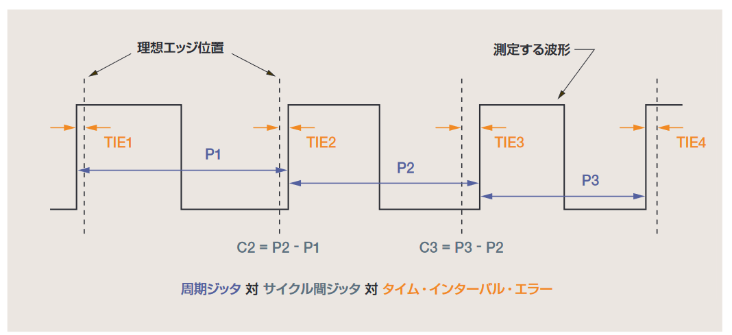
There are several ways to measure jitter on a single waveform, including period jitter, cycle-to-cycle jitter, and time interval error (TIE). Understanding how these measurements relate to each other and what they reveal is crucial. Figure 2.4a shows a clock signal with timing jitter. The dotted lines indicate the ideal edge positions in the absence of jitter.
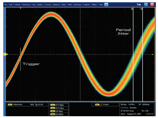
Period jitter, indicated by measurements P1, P2, and P3 in the figure, simply measures the period of each clock cycle of the waveform. This is the simplest and most direct measurement. Its peak-to-peak value can be observed by setting the oscilloscope's display mode to infinite persistence and adjusting it to display more than one clock cycle on the screen. When the oscilloscope triggers on the first edge, period jitter can be observed at the second edge, as shown in Figure 2.4b.
Cycle-to-cycle jitter, indicated by C2 and C3 in Figure 2.4a, measures how much the clock period varies between two adjacent cycles. As shown in the figure, cycle-to-cycle jitter can be detected by performing a first difference (differentiation) operation on period jitter. This measurement is sometimes important because it shows the amount of instantaneous jitter that the clock recovery PLL might experience. Measuring period jitter and cycle-to-cycle jitter does not require knowledge of the reference clock's ideal edge position.
Time interval error, indicated by measurements TIE1 to TIE4 in Figure 2.4a, measures how much the active edge of the clock deviates from its ideal position. To make this measurement, the ideal edge must be known or estimated. Therefore, it is difficult to observe TIE directly with an oscilloscope unless some form of clock recovery or post-processing is performed.
TIE can also be calculated by integrating period jitter after subtracting the nominal (ideal) clock period from each measured period. TIE is important because even small amounts of period jitter can accumulate over time to create large deviations from the ideal edge position. When TIE reaches ±0.5UI (unit interval), the eye closes, and bit errors occur in the receiver circuitry.
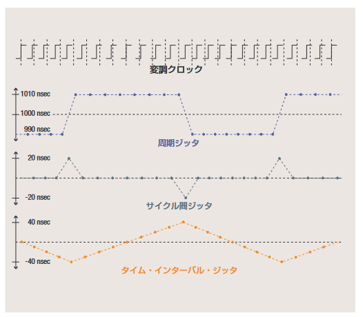
Figure 2.4c shows an example of comparing these three jitter measurements on a specific waveform. In this example, the nominal period of the waveform is 1μs, but the actual period is a pattern of eight 990ns cycles followed by eight 1010ns cycles.
Chapter 3: Jitter Measurement and Visualization
This chapter describes several tools and techniques useful for quantifying and analyzing jitter.
3.1 Jitter Statistics
Since signals contain jitter with random components, statistical methods are necessary for accurate jitter evaluation. Commonly used methods include:
Mean Value: The arithmetic mean value of clock periods, i.e., the mean value, is the nominal period. This is the reciprocal of the frequency measured by a frequency counter. The mean value of TIE is theoretically zero, but small residuals may appear depending on the measurement technique.
Standard Deviation: Represented by the Greek letter sigma (σ), the standard deviation is the average amount by which measurements deviate from their mean value. This is particularly useful when the distribution is represented by a Gaussian process where the distribution can be fully specified by the mean and standard deviation. This is detailed in "4.3 Composite Jitter."
Maximum, Minimum, and Peak-to-Peak Values: Generally, the maximum and minimum values are the actual observed values during the interval measurement. The peak-to-peak value is simply the maximum value minus the minimum value. These measurements must be used appropriately. In deterministic signals with regular variations, these values may equal the true values even after relatively short interval measurements. However, in random signals with Gaussian distribution, the theoretical maximum and minimum values have no limits, so the observed peak-to-peak value increases over time. Therefore, when using peak-to-peak values, knowledge of the population size and the nature of this type of distribution is required.
Population: The population refers to the number of individual measurements (events) included in a statistical data set. In random processes, a larger population intuitively provides greater confidence that the measurement results are reproducible. When the characteristics of the distribution are known or can be estimated, the population required to reduce measurement uncertainty to the desired point (set value) can be calculated.
3.2 Jitter Histogram
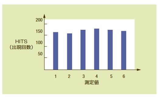
A histogram is a plot showing the distribution of occurrences (frequency of occurrence) of measurement values in a data set. When there are many measurements in a data set, the histogram can accurately estimate the PDF (probability density function) of the data set. For example, if you roll a die 1,000 times and record the results, the distribution will look like Figure 3.2a. The HITS axis represents the number of occurrences of each number. Note that the histogram is not related to the order in which the measurements were taken.
Figure 3.2b shows an example of a jitter histogram in a TIE measurement. In this case, the continuous variable (number of bins in the distribution) is mapped to 500 bins, and the total number of measurements (total events) in the data set is 3,200,000. Since this is a TIE measurement, the mean value is 0ns. In this plot, the distribution is approximately Gaussian with a standard deviation of 1.3ps.
Let's consider a second example. In this example, the TIE of the signal in Figure 3.2b is modulated by a sinusoidal wave, as shown in Figure 3.2c.

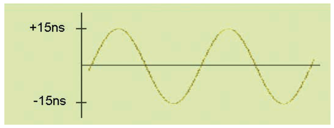
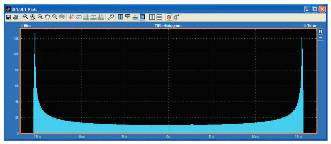
If you sample this sinusoidal wave at any point in time, the likelihood is equal, and the sample values will exist anywhere between -15ns and +15ns. Therefore, the TIE histogram of this modulated signal, as shown in Figure 3.2d, will be roughly uniformly distributed over ±15ns (the sloped edges on the left and right sides of the histogram indicate that the jitter still has Gaussian components).
3.3 Jitter and Time (Time Trends)
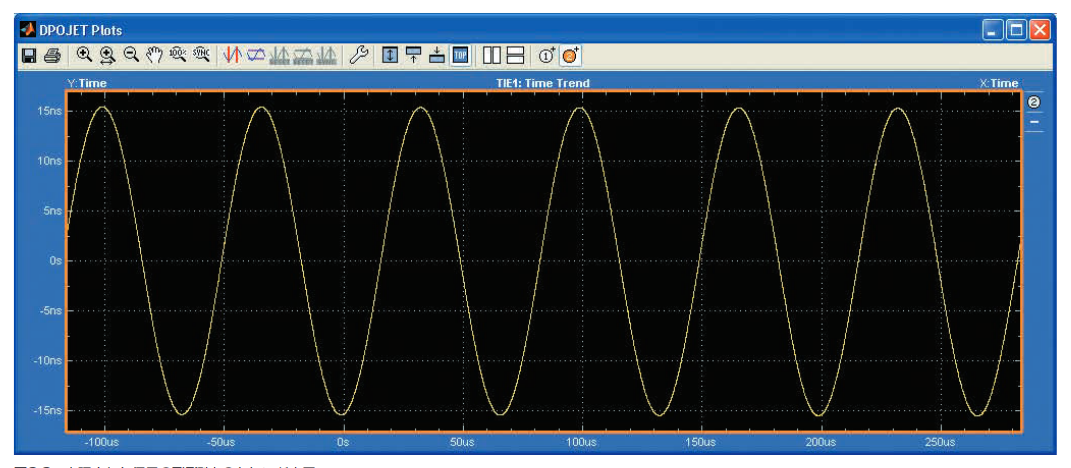
Since jitter histograms do not show the order in which measurements were taken, repetitive patterns indicating modulation or other periodic components are not apparent. These repetitive patterns become clear when jitter values are plotted against time. For example, if you plot the TIE of the phase-modulated signal in Figure 3.2d against time, it becomes Figure 3.3a. This reveals the jitter variation pattern, which may clarify the correlation with one of several jitter sources.
3.4 Jitter and Frequency (Jitter Spectrum)
Since jitter measurements can be plotted against time, applying Fourier transforms to these measurements allows the results to be displayed in the frequency domain. This becomes a jitter spectrum, with the modulation frequency on the horizontal axis and the modulation amplitude on the vertical axis. One advantage of spectrum analysis is that periodic components, which may be obscured by broadband noise, can often be clearly identified.
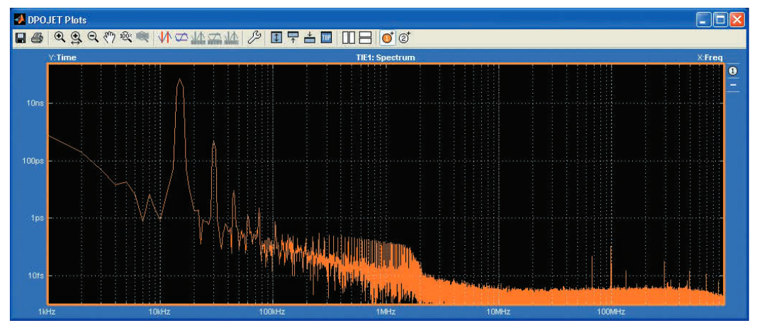
We reuse the example of the clock modulated by a sinusoidal wave mentioned earlier. Figure 3.4a shows the spectrum analysis of the TIE measurement in Figure 3.3a.
This clearly shows that the modulated signal has a fundamental frequency of 15kHz, as indicated by the large peak waveform. Although a 15kHz sinusoidal wave theoretically has only a fundamental component in the FFT, the TIE of the sinusoidally modulated clock contains harmonics, so harmonics at 30kHz, 45kHz, and 60kHz are observed. Random noise still appears but is displayed as a wide flat noise floor in this figure, flattening out above 2MHz.
As mentioned earlier, timing variations with Fourier components below the usual 10Hz limit are considered wander rather than jitter. Moreover, from a practical standpoint, other frequency limits (e.g., the loop bandwidth of the system's clock recovery loop) may determine which noise is safely tolerable. A jitter spectrum display clarifies whether the system noise will be problematic.
3.5 Eye Diagram
The methods discussed so far rely solely on edge positions, which are extracted from the waveform by detecting when the waveform crosses one or more amplitude thresholds. An eye diagram is a more general tool that allows observation of both amplitude and timing behavior of the waveform.
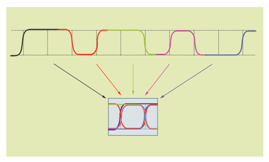
As shown in Figure 3.5a, an eye diagram is created by overlaying many short segments of the waveform so that each edge position and voltage level align. It is typically displayed with a horizontal span of 2 unit intervals. The waveform segments may be adjacent, as shown in the figure, or taken at wider intervals. If the waveform is a repetitive signal, an eye diagram can be created from individual samples taken at random delays on many waveforms using sampling.
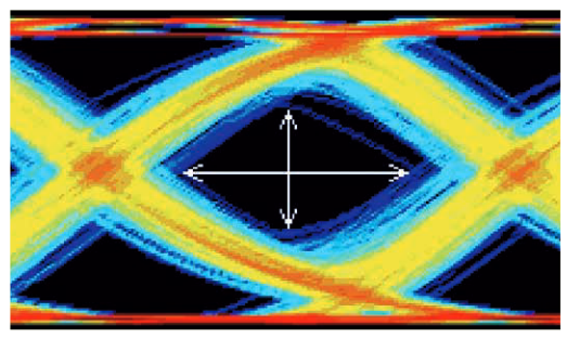
In Figure 3.5a, colors are used to show how individual waveform segments contribute to the eye diagram. In practice, eye diagrams are usually displayed in black and white or with colors indicating the sample density at any point on the screen. Figure 3.5b shows a color density display of a waveform with several types of noise.
The white arrows in the figure indicate the vertical and horizontal sizes of the eye opening. As the signal noise increases, the eye opening decreases horizontally, vertically, or both. If the center of the figure has no open area, the eye is said to be closed.
The simplest way to create an eye diagram is to use an oscilloscope in long persistence display mode. This approach requires attention to how the oscilloscope is triggered. Simply triggering on the waveform's edge results in an eye diagram relative to that edge, which may differ significantly from an eye diagram relative to the fundamental bit clock. Creating a bit-clock-based diagram requires some form of clock recovery in either software or hardware. If the oscilloscope does not have this feature, an external clock recovery circuit can provide the trigger.
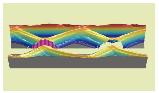
The relationship between the eye diagram and the TIE histogram can be seen by converting the density eye diagram in Figure 3.5b into a three-dimensional graph and slicing along the decision threshold, as shown in Figure 3.5c. The pink areas correspond to the first histogram of the two zero-cross points in the eye diagram.

Chapter 4: Jitter Decomposition
“All models are wrong, but some are useful.” W. Edwards Deming
Jitter decomposition, or jitter separation, is an analysis method that uses parameterized models to describe and predict system behavior . This chapter explains why this method is used and details the most commonly used jitter models today.
4.1 Purpose of Decomposing Jitter
It is often helpful to use mathematical models of the system to understand how a real system operates. The behavior of these models can be adjusted by tuning the parameters of each component. When the model parameters are chosen based on actual system observations, the model can be used to predict system behavior in other situations. Therefore, one purpose of jitter decomposition (also known as jitter separation) is to estimate system performance when direct measurement is difficult or time-consuming.
Another purpose of modeling the system this way is related to analysis. If each model component is associated with multiple fundamental physical effects, understanding the model can accurately identify the causes of excessive jitter.
Since the model of a complex system is simplified and based on assumptions, the degree of fit between the model and actual system behavior is not precise. In fact, when matching the model's behavior with actual measurements, there is always some tolerance in parameter selection. Therefore, jitter separation has some technical and scientific elements, and "99.99%" reproducibility of measurements is not expected.
4.2 Jitter Models
The most commonly used jitter model is based on the hierarchy shown in Figure 4.2. In this hierarchy, total jitter (TJ) is first divided into random jitter (RJ) and deterministic jitter (DJ). Whether these two types of jitter are accurately identified has a significant impact on the model's accuracy, more so than other modeling decisions.
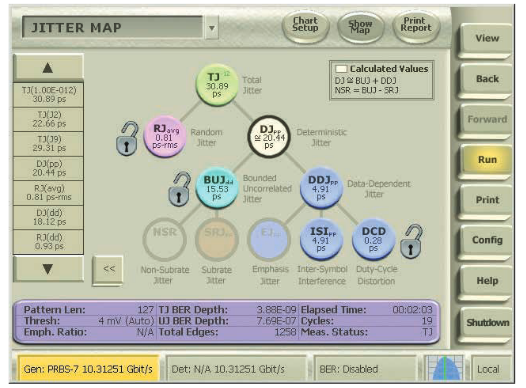
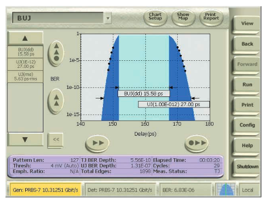
Deterministic jitter is further divided into periodic jitter (PJ, also called sinusoidal jitter, SJ), duty cycle dependent jitter (DCD), data-dependent jitter (DDJ, also called inter-symbol interference, ISI), and bounded uncorrelated jitter (BUJ). Figure 4.2a shows the BUJ values displayed by the BER contour function of the BERTScope.
The characteristics and root causes of each of these types of jitter will be discussed later.
4.2.1 Random Jitter
Random jitter is unpredictable timing noise with no identifiable pattern. A representative example of random noise is the sound heard when a radio receiver is tuned to a carrier frequency. For the purposes of jitter modeling, random jitter is assumed to have a Gaussian distribution because many sources of random noise in electrical circuits, such as thermal noise (also known as Johnson noise or shot noise), are known to have Gaussian distributions. A more fundamental reason is that the combined effects of many uncorrelated noise sources approach a Gaussian distribution according to the central limit theorem, regardless of the distribution of individual noise sources.
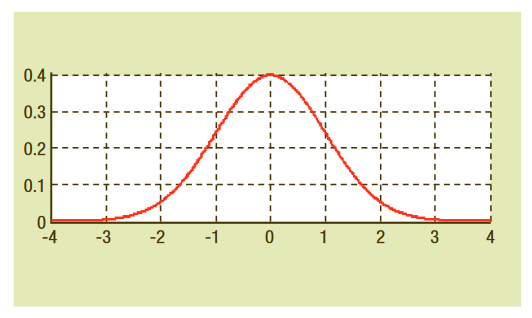
A Gaussian distribution, also known as a normal distribution, has a PDF represented by the familiar bell curve. Figure 4.2.1a shows an example of a Gaussian distribution with a mean value of zero and a standard deviation of 1.0. One of the most important characteristics of this distribution is that the peak value of a Gaussian variable is infinite, meaning most samples of this random variable cluster around the mean, but some specific samples can theoretically differ significantly from the mean. Therefore, the underlying distribution has no limited peak-to-peak value. The more samples taken from such a distribution, the larger the measured peak-to-peak value.
One approach to evaluating such a distribution is to repeatedly sample and record the resulting peak-to-peak values. This approach requires caution because the peak-to-peak value of N measurements of a random variable is itself a random variable. For example, using such a random variable as a pass/fail criterion for quality control may require raising the acceptance threshold due to measurement uncertainty, resulting in acceptable products failing. A better approach is to fit N measurements to the estimated distribution (in this case, a Gaussian distribution). This allows the use of the mathematical representation of the distribution to predict long-term behavior to a specific confidence level.
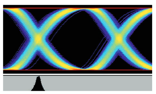
Figure 4.2.1b shows an eye diagram and the associated TIE histogram of a signal with Gaussian jitter.
4.2.2 Deterministic Jitter
Deterministic jitter is predictable timing jitter that can be reproduced. Therefore, the peak-to-peak value of this jitter is limited and can be observed and predicted with high confidence based on relatively few measurements. This type of jitter is classified as follows, based on its characteristics and root causes.

4.2.3 Periodic Jitter
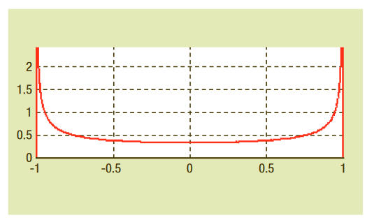
Periodic jitter is jitter that repeats periodically. An example is shown in Figure 2.4c. The time trend of TIE represents a repeating triangular wave. Since periodic waveforms can be decomposed into harmonics of sine waves by Fourier series, this type of jitter is sometimes called sinusoidal jitter. Figure 4.2.3a shows the probability distribution of a sine wave with a peak amplitude of 1.0.
Generally, periodic jitter is not correlated with periodically repeating patterns in the data stream. Jitter correlated with repetitive data patterns is discussed in the next section. Periodic jitter is caused by external deterministic noise sources coupled into the system, such as switching power supply noise or strong local RF carriers. It can also result from unstable clock recovery PLLs.
Figure 4.2.3b shows an eye diagram and the associated TIE histogram of a signal with 0.2UI of periodic jitter.
4.2.4 Data-Dependent Jitter
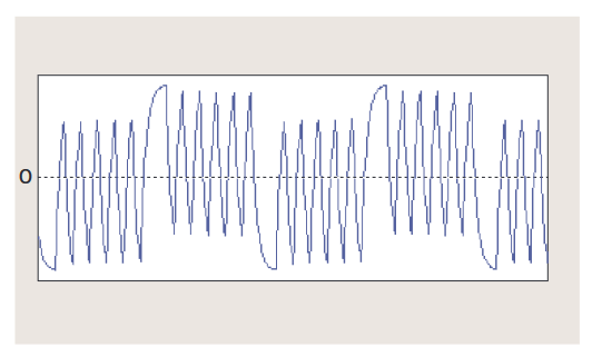
Data-dependent jitter, or DDJ, is jitter correlated with the bit sequence of the data stream. DDJ often occurs due to the frequency response of cables or devices. Let's consider the waveform in Figure 4.2.4a. The data sequence is strongly low-pass filtered. Due to this filtering, the waveform does not reach the complete high or low state unless the same polarity continues for several bits.
Figure 4.2.4b shows different waveforms of the data sequence overlaid. It can be observed that the falling transition crosses the threshold level earlier when followed by a 1,0,1,0,1,0,1 sequence than when followed by a 1,0,1,0,1,1,1 sequence.
This timing shift is predictable and related to the specific data before the transition, making it an example of DDJ, also known as inter-symbol interference, ISI.
Figure 4.2.4c shows an eye diagram and the associated TIE histogram of a signal with 0.2UI of DDJ. The histogram of ISI jitter always consists of impulses only.


4.2.5 Duty Cycle Dependent Jitter
Duty cycle dependent jitter (DCD) is predictable jitter based on whether the related edge is rising or falling. Common causes of DCD include the following:
- 1. The slew rate of the rising edge differs from the falling edge.
- 2. The decision threshold of the waveform is higher or lower than it should be.
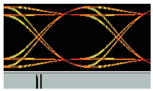
Figure 4.2.5a shows an eye diagram for the first case. The decision threshold is at the 50% amplitude point, but the rise time of the waveform is slower, causing the rising edge to cross the threshold later than the falling edge. As a result, the edge crossing histogram (in gray) shows two distinct groups (unlike the previous eye diagrams, this waveform example has Gaussian noise in addition to duty cycle dependent jitter).
Figure 4.2.5b shows an eye diagram for the second case. The rise and fall times of the waveform are balanced, but the decision threshold is not set at the 50% amplitude point. The edge crossing histogram is very similar to the histogram shown in Figure 4.2.5a.
4.2.6 Bounded, Uncorrelated Jitter (BUJ)
Crosstalk between adjacent channels in high-frequency serial links, such as 4x10GbE, significantly impacts the performance of serial links. Crosstalk can impair the accuracy of traditional jitter separation methods, resulting in excessive calculation of random jitter, reducing the design margin of high-speed link devices. Jitter separation provides a more accurate evaluation of eye synthesis resulting in BER, as shown in Figure 4.2.6.
4.2.7 Subrate Jitter (SRJ)
Deterministic jitter often occurs in systems due to nearby logic processing. This type of jitter, which results from such interactions, can be either synchronous or asynchronous, falling into the category of BUJ (bounded, uncorrelated jitter). Synchronous jitter with the clock is a typical case. Signal processing such as multiplexing/demultiplexing, channel coding, block formatting, and low-speed parallel processing can all shift edges at integer clock boundaries.
The 4:1 multiplexer of the transmitter, shown in Figure 4.2.7, advances or delays the timing of all registers' parallel loads at edges divisible by four. An eye diagram triggered at one-fourth of the clock rate shows two eyes with normal eye widths and one short eye width and one long eye width around jittery edges. This can be observed with all bits in the pattern (unless the pattern length is a multiple of four), so it is not interpreted as ISI.
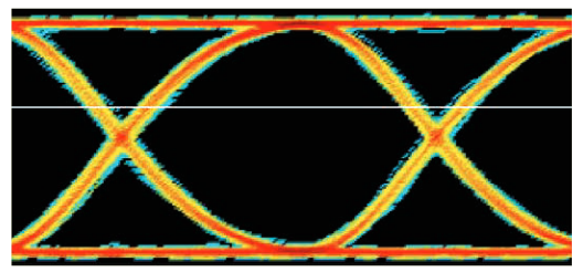
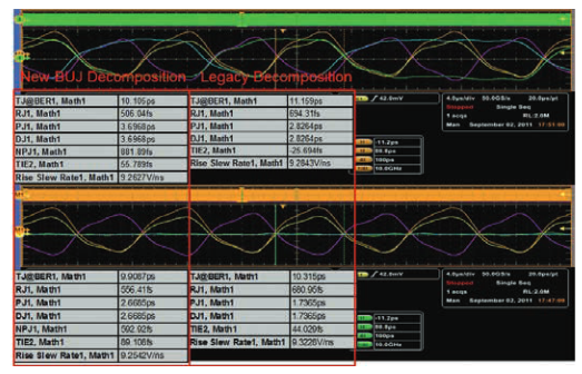

The above subdivision into factors related to the number of transitions per average interval indicates deterministic jitter with a correlation to the division ratio, which is reported as SRJ (Subrate Jitter). BUJ larger than the SRJ count is further called NSRJ (Non-Subrate Jitter).
Care must be taken to avoid confusing SRJ with pattern-dependent ISI. Jitter seen at the subrate divider is not included in the SRJ count, as the measured data pattern is recognized as an ISI component when it is exactly a multiple of the subrate division.
4.3 Composite Jitter
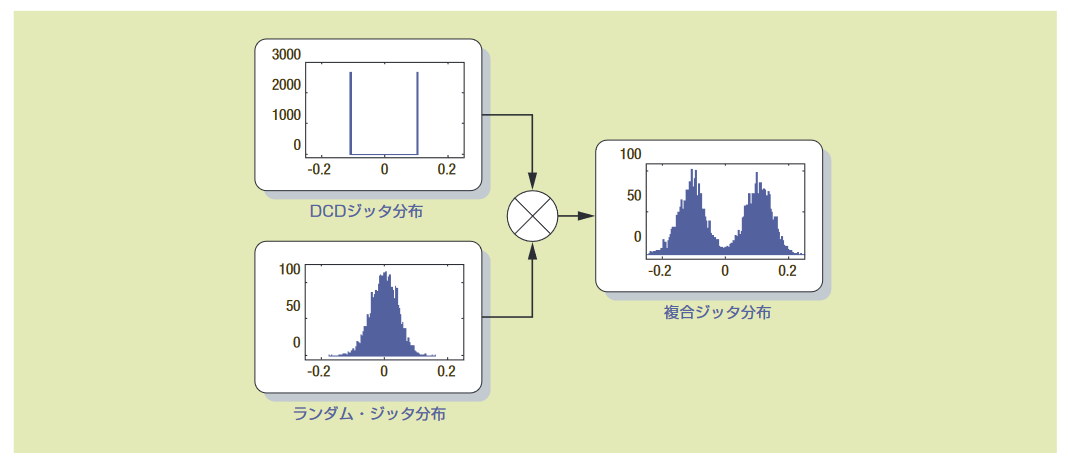
Previously, eye diagrams and TIE histograms for various types of jitter were discussed. However, what happens to the histogram when multiple types of jitter occur simultaneously? An effective and applicable result from statistical theory is that the combined effect of multiple uncorrelated processes results in a distribution equal to the convolution (convolution integral) of the individual distributions.
This concept is easier to understand with visual examples than with words. Figure 4.3a shows what happens when duty cycle dependent jitter (whose histogram consists of two impulses) combines with random jitter (which has a Gaussian distribution). Figure 3.2d also shows an example where a sinusoidal distribution (the same as a periodic jitter distribution) competes with random jitter.
Theoretically, by observing the final histogram in Figure 4.3a, it is possible to deduce what the two types of jitter cause. However, in real examples, the final histogram often becomes complex and difficult to intuitively recognize because it contains various amounts of all types of jitter. One of the purposes of detailed jitter analysis is to identify all the individual jitter components that cause the final result.
Jitter separation reveals its true power when accurately identified jitter components are applied to the jitter model shown in Figure 4.2, using the model to predict how the system will behave in a new environment. This is the basis for estimating bit error rates, detailed in Chapter 5.
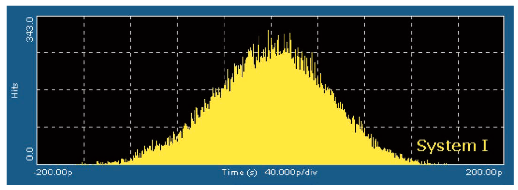
To understand why accurate analysis tools are essential, compare two systems with different jitter characteristics. Let's call the first system System I. This system has only random jitter with a standard deviation of 0.053UI. Figure 4.3b shows the TIE histogram of this system with a data rate of 1062.5Mbps.
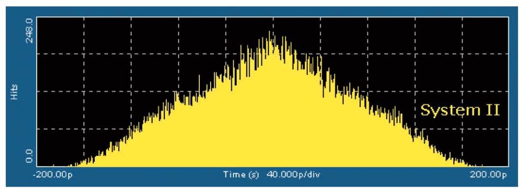
The second system is called System II. This system has random jitter with a standard deviation of about half that of the first system, 0.028UI. However, this system also has two uncorrelated periodic jitter components, each with a peak-to-peak amplitude of 0.14UI. Figure 4.3c shows the TIE histogram of System II.
These two histograms with the same event count of approximately 42,000 edges do not appear significantly different. In fact, for these two sample sets, the peak-to-peak TIE values are exactly the same at 430ps (0.457UI). If visual comparison is the only method available, it becomes difficult to distinguish between these two cases. Accurate prediction of how the system will perform over extended measurement intervals is impossible.
You may wonder whether it is important to distinguish between these two cases, given how similar they appear. After explaining bit error rate and bathtub curves, we will revisit this example.
Chapter 5: Jitter and Bit Error Rate
“An approximate answer to the right question is worth a great deal more than a precise answer to the wrong question.”
John Tukey
5.1 Jitter Budget
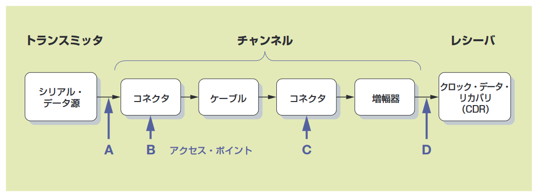
A practical communication system consists of a transmitter, a channel, and a receiver, as shown in the model in Figure 5.1. The channel may include cables, interconnects, and active devices without clock recovery. The channel can introduce filtering, nonlinearity, DC offsets, and further random jitter. Various circuit test points and system connectors become access points to evaluate signal quality. As the signal progresses from the transmitter to the receiver, signal quality is evaluated at each access point (perhaps using eye diagrams) in sequence, and jitter generally deteriorates.
One might simply assume that if the signal still has any eye opening left when it reaches the input of the receiver's clock data recovery circuit (access point D), the system will be successful. However, receiver circuits are not perfect. To ensure the signal eye provides sufficient timing margin for the receiver's data decision circuit, it must remain horizontally open and vertically open to accommodate noise affecting the decision threshold.
Thus, a complete system design specification allocates a jitter budget, with well-defined jitter limits at each access point, ensuring sufficient margin remains when the signal enters the receiver for resynchronization.
5.2 Bathtub Curve
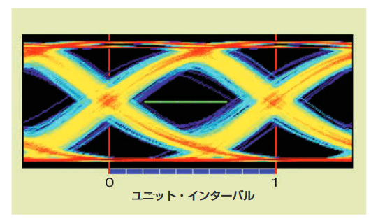
The concept of eye diagrams and eye openings was discussed in "3.5 Eye Diagrams." Gaussian probability distributions, which have theoretically unlimited peak-to-peak values, were covered in "4.2.1 Random Jitter." When these two concepts are considered together, an interesting idea emerges. For signals with Gaussian jitter, an eye diagram will completely close if samples are accumulated over a sufficiently long period. This makes the concept of eye opening as a basis for comparison useless. However, applying a confidence level to the eye opening allows the use of eye diagrams.
Let's consider Figure 5.2a. A green ruler 0.5UI long is placed horizontally at the center of the eye. Suppose we assume that any waveform crossing this ruler, whether on a rising or falling edge, is considered an error. Although the waveform does not seem to cross the ruler in this figure, if sampling continues, and the signal has Gaussian jitter, the waveform will eventually cross the ruler.
Instead, suppose we assume that if only 1 out of 1,000 waveforms crosses the ruler, the test is successful. Regardless of how long the test takes, it is no longer an issue. If 50,000 waveforms are accumulated and fewer than 50 cross the ruler, the test is passed. It can be said that the eye is 50% (0.5UI) open for a BER (bit error rate) of 10−3 if each crossing is assumed to represent a bit error.
If the same signal is tested with a shorter ruler, say 0.25UI long, the number of times it crosses the ruler will surely decrease. Perhaps on average, 1 out of 100,000 waveforms will cross this short ruler. It can be said that the eye is 25% (0.25UI) open for a BER of 10−5.
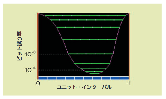
This method of using rulers accurately evaluates eye opening for a given bit error rate (note that each ruler can slide left and right to achieve the best fit). If all rulers are plotted on one chart against the corresponding bit error rate and the ends of the rulers are connected by lines, the graph will look like Figure 5.2b.
Because the pink line looks like a bathtub, this distribution graph is called a bathtub curve. This graph shows the region where no signal transitions occur within the eye horizontally at a given confidence level (the size of the eye opening).
Finally, note that it may take a long time to accumulate enough data to measure the eye opening near the bottom of the chart. Therefore, mathematical models discussed in Chapter 4 are used to predict performance based on much smaller sample sets.
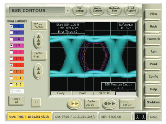
Another concept that helps identify jitter performance at a specific BER level is plotting BER contours. BER contours (Figure 5.2c) extend the bathtub curve concept by measuring the eye opening radially and clearly representing eye openings at specific BER levels.
5.3 BER Examples
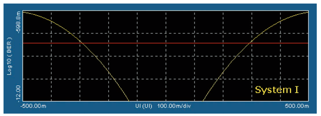
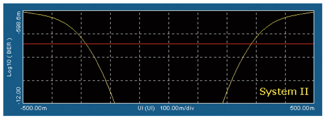
In "4.3 Composite Jitter," an example was given of two systems with different jitter characteristics that have nearly identical TIE histograms and peak-to-peak jitter characteristics at a sample size of approximately 42,000 edges (see Figures 4.3b and 4.3c). Here, we return to that example and show the related bathtub curves. Figure 5.3a shows the bathtub curve for System I, and Figure 5.3b shows the bathtub curve for System II.
Both graphs represent the same data set of 42,000 observed edges, with red cursors placed at the position corresponding to the BER of 10−4.63 on each graph. At these levels, both systems show about a 58% eye opening, with System I's eye opening actually larger than System II's. However, at BER 1e-12 (a frequently used regulation point for serial communication links), System I's eye is only 26% open, while System II's eye is 37% open, about 1.5 times larger. This is a significant difference, easily determining whether the system meets the specification at the specified BER.
Chapter 6: Summary
Timing jitter always degrades electrical systems, but the importance of its evaluation is increasing to achieve higher data rates and narrower logic widths. Evaluation is necessary to identify the cause of jitter and reduce it through redesign. It also helps in defining, identifying, and measuring jitter for compliance with standards and design specifications.
Jitter has random and deterministic components. Due to its random nature, specifying acceptable limits for jitter requires caution, particularly when predicting jitter performance at low error rates based on relatively small data sets. The best approach for handling the random component of jitter is to use mathematical models for analysis and prediction, with parameters adjusted based on observed measurements. These models can be used to predict performance in other situations and to identify the causes of jitter, helping to understand which components of jitter need to be reduced.
Oscilloscopes have long been tools for observing jitter using techniques such as histograms and eye diagrams. Enhanced oscilloscopes with backend processing features like cycle-to-cycle measurements, time trends, spectrum plots, data logging, and worst-case capture are optimal tools for evaluating timing jitter. Additionally, oscilloscopes with advanced clock recovery, jitter separation algorithms, and bit error rate prediction are the only solutions for evaluating and reducing timing jitter.
Best Oscilloscopes for Jitter Measurement
Introducing the latest oscilloscopes, the only solution for measuring, evaluating, and reducing timing jitter.
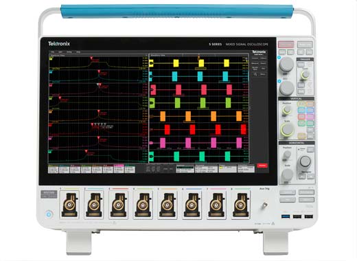
5SeriesB MSOMixed Signal Oscilloscope
With superior waveform fidelity, diverse measurement displays, unique spectrum analysis, and flexible probe technology, you can grasp the overall picture of the design. Experience the intuitive user interface supported by engineers worldwide.
6SeriesB MSOMixed Signal Oscilloscope
Troubleshooting and verification of high-speed designs with a bandwidth of 1GHz to 10GHz. Achieve accurate measurements with low noise and a maximum sample rate of 50GS/s. Detailed analysis of designs is possible with 6-channel and 8-channel models.
DPO70000SX ATIPerformance Oscilloscope
The DPO70000SX Series ATI Performance Oscilloscope captures high-speed signal behavior with excellent accuracy, making it ideal for verifying, validating, and characterizing next-generation designs. Capturing signals up to 70GHz with low noise and excellent fidelity, it enables highly accurate measurements and precise signal characterization.
Appendix A: Glossary of Abbreviations
BER Bit Error Rate
BUJ Bounded, Uncorrelated Jitter
CDF Cumulative Distribution Function
DCD Duty Cycle Dependent Jitter
DDJ Data-Dependent Jitter
DJ Deterministic Jitter
FFT Fast Fourier Transform
ISI Inter-Symbol Interference
NSRJ Non-Subrate Jitter
PDF Probability Density Function
PJ Periodic Jitter
PLL Phase-Locked Loop
PSD Power Spectral Density
RJ Random Jitter
SJ Sinusoidal Jitter
SRJ Subrate Jitter
TIE Time Interval Error
TJ Total Jitter
UI Unit Interval


