AC-DC power supplies, especially those designed to comply with IEC61000-3-2 or ENERGY STAR standards, often include some form of active power factor correction (PFC). This application note describes procedures for using an oscilloscope to measure power factor using both manual and automated power analysis software on an oscilloscope. It covers harmonics measurements using FFT, as well as using power analysis software. Finally, it outlines the unique challenges around measurements for characterizing the performance of the switching device within the PFC circuit and explains how power analysis software can help make these measurements consistently and accurately.
Power factor correction circuits reduce the negative impacts of AC-DC converters on the power distribution system. In a conventional non-PFC power supply, the rectified AC voltage charges a large filter capacitor. During much of the mains power cycle, the diodes are reverse-biased and do not conduct. Therefore, the power supply draws current from the power line only in a short pulse when the AC input voltage exceeds the capacitor voltage. These short pulses generate harmonics of the mains frequency and result in a low power factor. Excessive current harmonics can adversely affect nearby devices, and low power factor raises the cost of the required mains distribution system.
Power Factor (PF) of an AC power system is defined as the ratio of the real (also called “true”) power (in Watts) flowing into the circuit to the apparent power (in VoltAmps) in the circuit. Power factor is a dimensionless number which ideally has a value of 1.0 for the input of a power supply

Real power is a measure of the work the circuit can do in a given time period. The apparent power is simply the product of the voltage and current. Whether due to energy storage in the circuit or non-linearities in the load, which distort the current waveform, the apparent power often significantly exceeds the real power drawn by the load.
Power Factor Correction Operation
Active Power Factor Correction (PFC) is a method of increasing a device’s power factor using active circuitry to shape the current drawn by the device to make the load appear to be purely resistive at low frequencies. The effect is that the shape of the input current more closely matches the shape and phase of the input voltage, and the real and apparent powers become nearly equal.
For some low-power applications, say <75W, passive input filtering may be sufficient to improve the power factor, typically to a value of 0.7 to 0.85. A passive PFC can reduce the phase shift between the input current and voltage and broaden the current pulses, improving the power factor and reducing the harmonics generated.
However, in most other applications, an active PFC is used.In addition to significantly improving the device’s power factor and controlling the current harmonics, a boost PFC (used in the majority of PFC designs) can often automatically adjust to operate on AC voltages from 100V (in Japan) to 240V (in Europe and many other regions).
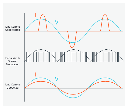
At a basic level, active power correction works by modulating the current waveform to shape it into a sine wave and align it with the voltage waveform, thus reducing harmonic content and increasing power factor. This is shown in Figure 1.
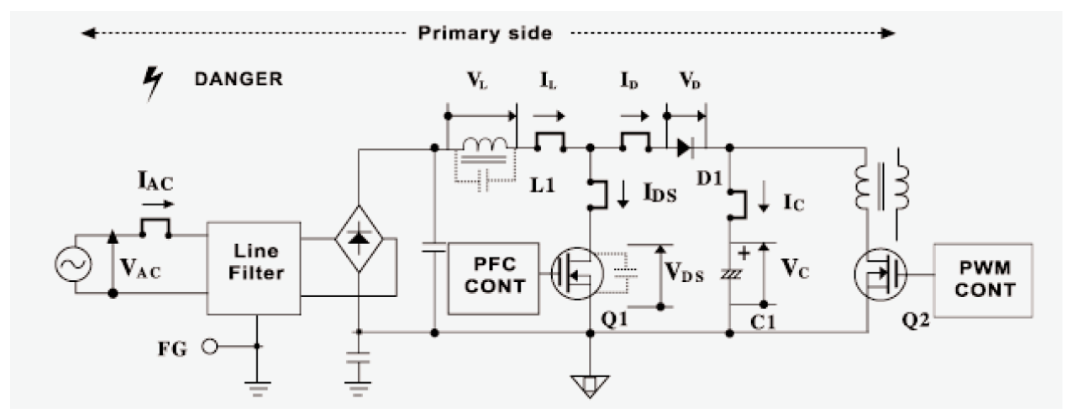
In the example switch-mode power supply used in this technical brief, a boost converter has been inserted between the input bridge rectifier and the main input capacitor. (See Figure 2.) The boost converter works to maintain a constant DC voltage across the capacitor while drawing a mains current that is in phase with the mains voltage. A switch-mode DC-toDC converter generates the output DC voltage(s) from the DC output of the boost converter.
A circuit diagram of the primary side of a switch-mode power supply with an active PFC circuit is shown in Figure 2. In this circuit, the MOSFET Q1 is controlled by a 100 kHz switching signal whose duty cycle is varied to ensure that the current flowing through inductor L1 is in phase with the line voltage.
When the MOSFET switch Q1 is on, diode D1 is off, and the current flowing through inductor L1 increases. Then, when Q1 is off, the current flowing through L1 charges capacitor C1 through diode D1. The output of the PFC circuit, the voltage across capacitor C1, is the high DC voltage that the DCDC converter then uses to generate the desired DC output voltages.
Measuring Power Factor
The ultimate test of the PFC is the measurement of the power factor of the loaded supply. For testing, the DC load is often a programmable electronic load, such as the Keithley 2380 Series. This allows testing under various load conditions.
EQUATION 1.

To measure power factor with an oscilloscope,
- Connect a voltage probe to line voltage and a current probe to line current.
- Select Cursor Gating for all measurements, and position the cursors to coincide with an integer number cycles of the mains voltage, and turn on automatic RMS Voltage and RMS Current measurements.…
- Or, if your oscilloscope provides cycle-based automatic measurements, activate the automatic measurements for Cycle RMS Voltage and Cycle RMS Current.
- Use waveform math to multiply the voltage and current waveforms point-by-point, to see the instantaneous power waveform.
- Activate the Cycle Mean automatic measurement on the power waveform.
The power factor may then be calculated using Equation
1. An example of this is shown in Figure 3, where the automatic measurements are used to determine the average instantaneous power of 174.3 W, RMS voltage of 120.2 Vrms,and RMS current of 1.478 Arms. Using Equation 1 this yields a power factor of 98.1%.
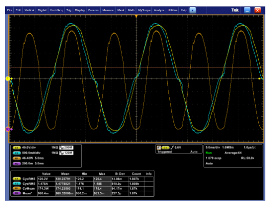
If your oscilloscope is equipped with power analysis software, the software automates the measurement. In Figure 4, the waveform display at the top of the screen shows that the corrected AC input voltage and current are in-phase and nearly identical in shape. The automated power quality measurements provide readouts of RMS voltage and current, voltage and current crest factors, line frequency, apparent power, true power, reactive power, and phase angle. Most importantly, for the PFC verification, the Power Factor measurement (0.993) verifies that the PFC is working as expected.

Measuring Current Harmonics
One of the key purposes of the PFC is to achieve nearly unity power factor which reduces the harmonic content of the current drawn from the power grid. These harmonics cause overheating of transformers and inefficiency in the power distribution system due to harmonic-related currents causing voltage drops in the transmission lines.
A quick check can be done using the FFT function on the scope, as shown in Figure 5. However this will not correlate with standards tests, since those tests generally evaluate harmonics based on discrete frequency bins around multiples of the line frequency.
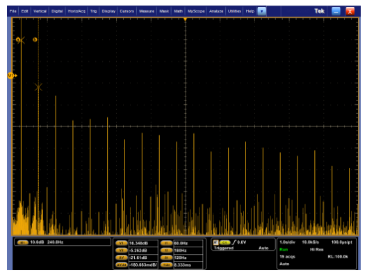
For harmonics measurements, power analysis software is a much better alternative.
The input characteristics of the power supply are analyzed by measuring the AC input voltage (VAC in Figure 2) and current (IAC).
Figure 6 shows a plot of the input current harmonics (green bars) relative to the EN61000-3-2 limits (gray bars). The cursor (orange diamond) provides numeric readouts of the individual harmonics.
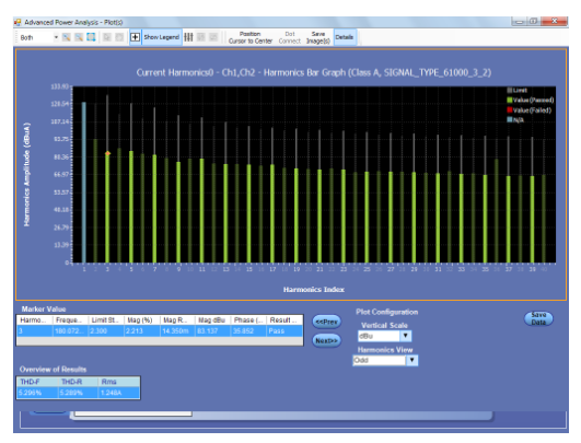
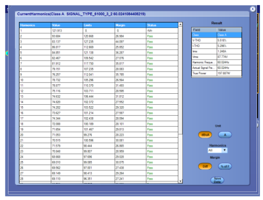
Figure 7 shows the same IEC 61000-3-2 Current Harmonics measurements and pre-compliance pass/fail status in a tabular form, along with the RMS voltage and current measurements,Total Harmonic Distortion (THD), fundamental frequency, and total power dissipation.
Making Measurements on the Switching Device
The addition of PFC to a power supply does wonders for power factor and harmonics, but at the cost of some efficiency loss. An understanding of the losses at each stage is important to optimize efficiency, thermal designs, and product reliability.
PFC circuit measurements present several significant challenges.
- You must be able to measure the high voltages and currents in the circuit, safely, accurately, and without affecting circuit operation. Simply connecting to the signals may be difficult. And measuring currents often requires adding current loops or sense resistors to the circuit. And many of the required measurements are not referenced to earth ground, so probes designed for safe power measurements are required.
- Voltage and current measurements on switching devices have very high dynamic range. You must be able to measure very large and very small signals at the same time.When a switching device is off, the voltage across it may be hundreds or thousands of volts, but the current through it is nearly zero. When the device is on, the current through it may be very high, but the voltage may be in the range of millivolts.
- You must be able to characterize a broad spectrum of signal frequencies, from line or mains frequencies (50 or 60 Hz) to switching frequencies (tens of kilohertz to megahertz). When measuring switching devices, an even more important characteristic is the switching rise time.This range of frequencies and rise times requires that the measurement equipment provide high real-time bandwidth,high sample rate, and long record lengths.
- Measuring switching behavior on Power Factor Correction circuits can be even more challenging to measure than simple buck convertors, since the control signal is modulated continuously over the AC line or mains cycle.
Finally, you must make many complex measurements,consistently and repeatably. Automation of power measurements is key to measurement efficiency and repeatability
This application note focuses on the distinct challenges you face when testing power factor correction circuits.However, many of the important considerations for power supply measurements are also important for testing PFC circuitry.
These considerations include:
- Making connections to the circuit
- Eliminating offset errors in voltage and current probes
- Correcting time skew between voltage and current probes
These application notes, available for download from Tek.com, give detailed information on addressing these considerations:
- Measuring Power Supply Switching Loss with an Oscilloscope
- Making Accurate Current Measurements on Power Supplies with Oscilloscopes
- Probing Techniques for Accurate Voltage Measurements on Power Converters with Oscilloscopes
Modulation Analysis on the PFC Control Signal
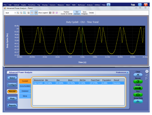
For unity power factor, the line current must be in phase with the line voltage. To achieve this, the PFC switching device turns on for a minimum period when that line voltage is at its peak and turns on for a maximum period when the line voltage is near zero. Between these extremes in line voltage, the conduction period is varied to ensure the PFC maintains a constant output voltage.
Viewing and measuring this variation in conduction period across a cycle of line voltage can be difficult. Using the modulation analysis capability of the power measurement application, you can plot the variations in the switching signal duty cycle, period, or frequency.
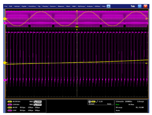
The VGS voltage, which is labeled PFC Control in Figure 1, is typically an ungrounded measurement, and thus requires a differential voltage probe. Figure 8 shows a display of the gate voltage waveform along with the line voltage and Figure 9 shows the plot of the duty cycle measurement on a similar time scale. The minimum duty cycle occurs during the peaks of the AC input voltage, and the maximum duty cycle points occur when the AC input voltage is very low.
Switching Loss Measurements
The Tektronix application note, “Measuring Power Supply Switching Loss with an Oscilloscope” gives detailed procedures for measuring switching loss.
However, switching loss measurements in a PFC circuit present special challenges, since the duty cycle of the switching waveform varies across the period of the AC input cycle. In this case, a gated measurement is used to ensure that the switching loss is fully characterized. Again, power analysis software greatly simplifies these measurements.
The voltage measurement will be made from the Drain to the Source of the switching MOSFET (VDS in Figure 1) or the Collector to the Emitter of a BJT or IGBT. Because these voltages may not be referenced to ground, a high-frequency, high-voltage differential probe provides the safest and easiest way to make this measurement. The switching current measurement will be made by measuring the current flowing into the Drain of the MOSFET (IDS in Figure 1) or the Collector current of a BJT or IGBT. This current may be measured with an AC/DC current probe or as a differential voltage drop across a shunt resistor.
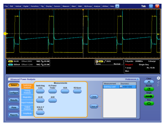
After the voltage probe and current probe have been properly connected, zeroed, and deskewed, Figure 10 shows the voltage (yellow channel 1) and the current (cyan channel 2) waveforms in the upper half of the display. The bottom half of the display shows the measurement selection control window in the advanced power measurement application.
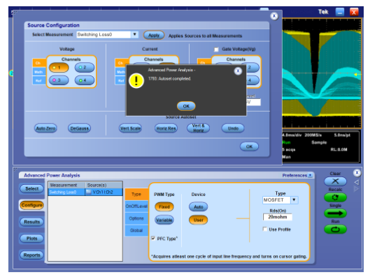
The power application’s Source Autoset optimizes the oscilloscope setup to accurately measure the switching signals, as shown in Figure 11. Analog bandwidth filtering and HiRes boxcar averaging are turned on to reduce random noise and improve vertical resolution. Finally, the horizontal scale, sample rate, and record length are set to acquire the appropriate time window at a high timing accuracy
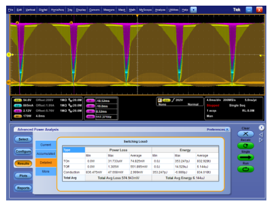
The average switching losses provide an accurate indication of the circuit dissipation (for example, for verifying the thermal or heatsink design), while the maximum switching losses are used to verify that the switching component is operating within the device’s absolute maximum ratings (the safe operating area).
Figure 12 shows the switching loss measurement results,including power and energy losses for the turn-on, turn-off,and conduction regions.
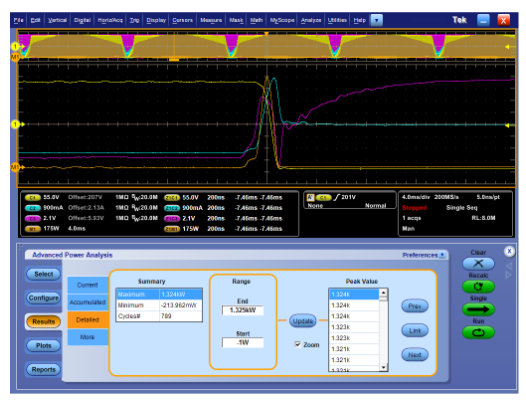
Switching loss measurements provide average power measurements for each of the switching regions and this can be very helpful when optimizing switching efficiency. However, it is also critical to identify the peak power losses. In a PFC circuit, the power losses vary widely across the AC input cycle and it can be time-consuming to find the maximum power points. DPOPWR Power Analysis Software has a HiPower Finder that quickly identifies the highest power loss in the complex instantaneous power waveform. Figure 13 shows an example of this measurement.
Safe Operating Area and Dynamic On-Resistance Analysis
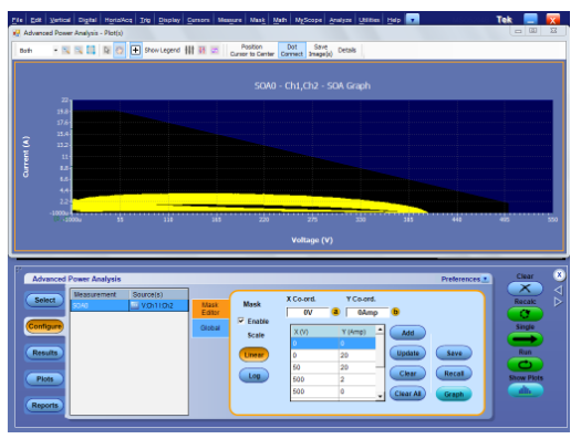
DPOPWR provides other important switch component measurements. Safe Operating Area (SOA) analysis provides pass/fail testing of the switching device operation by overlaying an SOA mask on an X-Y display of device voltage and current. The SOA mask is often given in the switching device data sheet, or it can be easily constructed with the specifications given in the data sheet.
As shown in Figure 14, the top of the mask is set to the absolute maximum drain current (IDmax), the right side is set to the drain-to-source breakdown voltage (VDSS), and the angled side is set to the absolute maximum power dissipation (PD). The SOA plot provides a simple visual indication of margin as the power supply is tested over its full operating range. In this test, the switching device is operating well within the safe operating area. For more on Safe Operating Area, read “Performing Safe Operating Area Analysis on MOSFETs and Other Switching Devices with an Oscilloscope”, available for download on Tek.com.
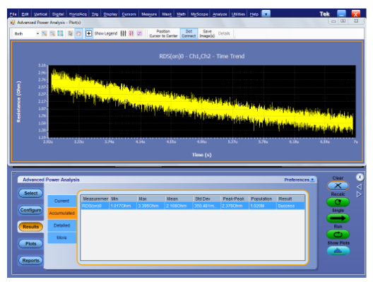
Although the majority of the losses in a switching device tend to be turn-on and turn-off losses, the conduction losses may also be significant. In the case of a MOSFET switching device, the device appears as a low resistance. Therefore, conduction losses are a function of the drain current and the resistance. The ratio of VDS to ID during the conduction cycle is the dynamic on-resistance.
Figure 15 shows the results of over a million automated RDSon measurements. During the middle of the conduction cycle, the MOSFET’s dynamic on-resistance consistently varies between about 2.5 and 1.5 Ohms.
In-circuit Measurements on Magnetic Components
As shown in Figure 2, the inductor L1 is a key storage device in the boost converter circuit.
Power analysis software makes it possible to quantify inductor performance under actual operating conditions. This is in contrast to using an LCR meter or dedicated B/H analyzer which measure magnetic properties under constant conditions using sine waves and small signals.
Figure 16 shows a measurement of the voltage across inductor L1 and the current through the inductor, which produces the B/H curve produced under rated load conditions. The power measurement software can also simultaneously calculate the inductance value and the total losses in the inductor in the actual circuit over the full operating range of the power supply.

Conclusion
The oscilloscope, advanced power analysis software, highvoltage differential probe, and current probe make it easy to safely capture power signals and provide repeatable complex component and power measurements to easily analyze the PFC circuit in a switch-mode power supply.
(Measurements and screen shots in this technical brief were made with a Tektronix 2 GHz MSO5204B oscilloscope equipped with the DPOPWR power measurement application, a 200 MHz TMDP0200 high-voltage differential probe, and a 120 MHz TCP0030A AC/DC current probe.)
Find more valuable resources at TEK.COM
Copyright © Tektronix. All rights reserved. Tektronix products are covered by U.S. and foreign patents, issued and pending. Information in this publication supersedes that in all previously published material. Specification and price change privileges reserved. TEKTRONIX and TEK are registered trademarks of Tektronix, Inc. All other trade names referenced are the service marks, trademarks or registered trademarks of their respective companies.
04.16 46W-60484-0


