Contact us
Live Chat with Tek representatives. Available 6:00 AM - 4:30 PM
Call us at 1-800-833-9200
Available 6:00 AM – 5:00 PM (PST) Business Days
Download
Download Manuals, Datasheets, Software and more:
Feedback
PCI Express® Transmitter Compliance/Debug Solution
DPO-MSO70000 Option PCE6, PCE5, PCE4, and PCE3 Datasheet
More Information
- Product Support
- Máy hiện sóng hiệu suất DPO70000SX ATI
- Máy hiện sóng lân quang số/tín hiệu hỗn hợp MSO/DPO70000DX
- Explore more Software models
Read Online:
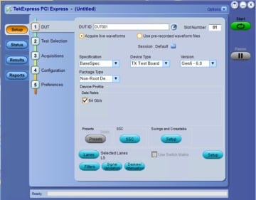


The PCI-SIG 6.0 specification has introduced PAM4 signaling to achieve 64 GT/s while maintaining NRZ signaling for backwards compatibility. The multilevel (PAM4) approach brings new signal integrity challenges to adopters and validation teams. Tektronix PCI Express 6.0 software minimizes this new complexity to automate testing and ensures measurement accuracy and repeatability.
The Tektronix Option PCE6 (Gen6), Option PCE5 (Gen5), Option PCE4 (Gen4), and PCE3 (Gen 1/2/3) applications provide the most comprehensive solution for PCI Express Transmitter and Reference Clock compliance testing as well as debug and validation of PCI Express devices against the PCI-SIG® specifications.
Features and benefits
- Support for PCI Express Gen6 Base (silicon) transmitter testing
- PCI Express Gen 1/2/3/4/5 validation and compliance of Transmitters at the BASE (silicon) and CEM (system) levels for the Tektronix DPO/MSO70000 Series oscilloscopes
- Reference Clock jitter and signal integrity measurements for Gen1 to Gen5 using SkyWorks Clock Jitter Tool and DPOJET
- 64 GT/s (PAM4) signal integrity measurements using DPOJET/PAMJET
- PCIe Gen6 Tx Equalization Preset test using AC Fit Method
- Automation fully configures the oscilloscope including the vertical and horizonal scales for accurate and specification compliant measurements
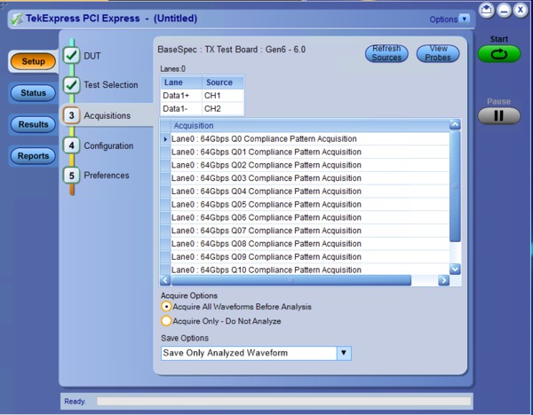
- Automated acquisition and waveform management to simplify testing across supported data rates, Tx compliance patterns, and lane widths
- Automated DUT control to step through data rates and compliance patterns
- RF switch automation of PCIe3 test solution, supporting up to x16 lanes
- Support for NVMe and CXL physical layer testing
- De-embedd the impact of a break-out channel, test fixtures, and cables to achieve measurements at the test point of interest (requires Option SDLA Serial Data Link Analysis)
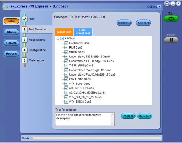
- Test selection: Select the specification against which to perform the analysis, and select individual tests or groups of tests to perform targeted compliance analysis for failing tests
- SigTest integration: Uses SigTest EXE (using command line interface) to perform the analysis of acquired waveforms, providing the ability to test a system using the PCI-SIG®-recommended analysis tool
- Analysis of multiple waveforms are done in parallel using multiple sigtest instances
- AC Fit Tx EQ Preset characterization for Gen5 with SigTest Phoenix
- Reporting: Compiles all test results into a customizable report with Pass/Fail results for easy analysis and record keeping
- Summary table at the top of the report for quick glance of results for normative measurement
- Pattern matching: Verifies that the correct set of compliance patterns are sent by the transmitter before acquiring signals for compliance analysis. This feature is supported up to Gen3 data rates
- PHY level protocol decode: Decodes and displays the PCIe data in a protocol-aware view. A time-correlated event table view with waveforms allows for quickly searching through events of interest
- Multi-lane testing: Perform analysis on multiple lanes of PCI express data to speed up the Tx analysis in a multi-lane system
- Compliance and debug: Provides a toolkit of DPOJET-based setups to quickly switch into debug and validation mode when a DUT fails compliance
- Analysis and debug tools: Tektronix provides a broad range of compliance, debug, and validation tools for Transmitter (Tx), Receiver (Rx), and protocol testing
- Comprehensive programmatic interface: Enables automation of programs and scripts to call PCIe related TekExpress functions
Applications
Tektronix provides the most comprehensive solutions for validation and compliance of PCI Express transmitters at the Base (silicon) and system level including support for CEM, U.2, and M.2 interfaces. Numerous protocols utilizing the PCI Express physical layer including NVMe and CXL can take advantage of the transmitter and reference clock automation under TekExpress software solution.
The Tektronix Option PCE3 (Gen1/2/3), PCE4 (Gen4) and PCE5 (Gen5) includes compliance and debug testing and electrical validation for the following:
- Root complex base Tx jitter and voltage
- Endpoint base Tx jitter and voltage
- Switches
- Bridges
- Add-In cards
- System boards
- Embedded systems
- Express module
The Tektronix Option PCE3, PCE4 and PCE5 applications include a TekExpress™ compliance automation solution that integrates SigTest from the PCI-SIG as well as Tektronix DPOJET-based PCI Express Jitter and Eye Diagram analysis tools for debug purposes in a single software package.
The Tektronix Option PCE6 (Gen6) includes the following signal quality measurements:
- Unit Interval
- V-TX-DIFF-PP
- V-TX-EIEOS-FS
- T-TX-UTJ
- T-TX-UDJDD
- T-TX-RJ
- RLM-TX
- SNDR
- PS21 TX
- V-TX-BOOST
- T-TX-UPW-TJ
- T-TX-UPW-DJDD
- V-TX-AC-CM-PP
- V-TX-AC-CM-PP-Filtered
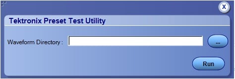
The PCIe Gen6 has two pre-shoot and one de-emphasis value for each preset complicating the preset test algorithm. The Tektronix PCE6 also comes with Tektronix Preset test tool, which can be used either by TekExpress or manually.
TekExpress compliance automation is available now for PCIe Gen 1-3 CEM and Gen 3 Base via Option PCE3, Gen4 CEM and Gen4 Base via Option PCE4, and Gen5 CEM and Gen5 Base via Option PCE5.
The Tektronix Option PCE3, Option PCE4, and Option PCE5 applications are compatible with Tektronix DPO/MSO70000 series oscilloscopes that are designed to meet the challenges of the next generation of serial data standards such as PCI Express. These oscilloscopes provide industry competitive vertical noise performance with the flattest frequency response for oscilloscopes in their class. The Tektronix DPO/MSO70000 series of oscilloscopes have been approved by PCI-SIG for compliance testing.
Compliance testing
The PCI-SIG provides PCI Express compliance tests for testing PCI Express systems and add-in cards. For a PCI Express system or a device to be placed on the Integrators List, the system or device must pass interoperability and compliance testing. For electrical validation, the PCI-SIG uses SigTest Post Capture Analysis Software that uses acquisitions from an oscilloscope connected to the PCI-SIG's CBB (main board + riser) test fixture for add-in cards or CLB test fixture for systems to perform the analysis. Manually capturing the required waveforms and analyzing them is tedious, time consuming, and error prone.
The Tektronix Option PCE3, Option PCE4, and Option PCE5 TekExpress Automation for PCI Express Transmitter Compliance reduces the effort and accelerates the compliance testing for PCI Express systems and devices with several unique and innovative capabilities. These options ultimately allow the testing of devices that support various technologies, such as NVMe, which is supported as an add-in card device, or through a U.2 or M.2 connector.
The Tektronix Option PCE3, Option PCE4, and Option PCE5 TekExpress Automation software can control the DUT using selected models of a Tektronix AFG or AWG, GRL PCIE 3/4 Controller or NI USB6501 CBB controller to toggle DUT and automatically cycle it through various speeds, de-emphasis, and presets that are necessary for the compliance test. This eliminates the error-prone manual push button approach normally used for DUT control on the CBB and CLB test fixtures.
A complete test run requires multiple waveforms to be acquired at different DUT settings per lane. This waveform set will increase by the number of lanes that need to be analyzed. The ability to manage and store the required data for analysis and future reference is an important criterion for any compliance solution. The Option PCE3, Option PCE4 and Option PCE5 TekExpress automation software, apart from adjusting the horizontal and vertical settings as well as the acquisition depth for optimal signal quality for accurate analysis, provides easy analysis to manage multiple acquired waveforms.
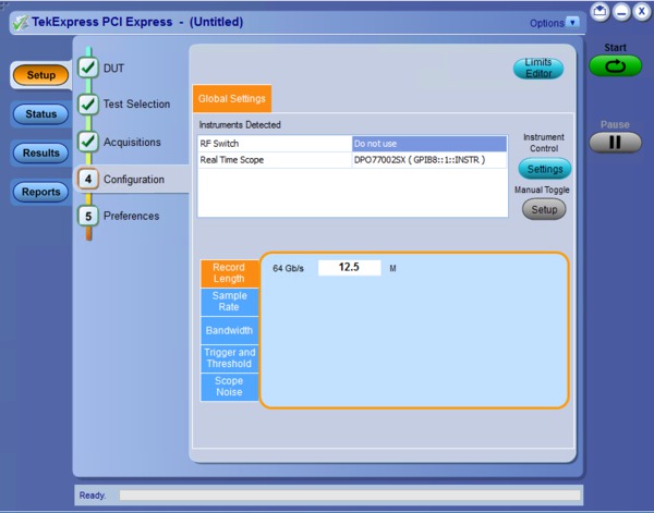
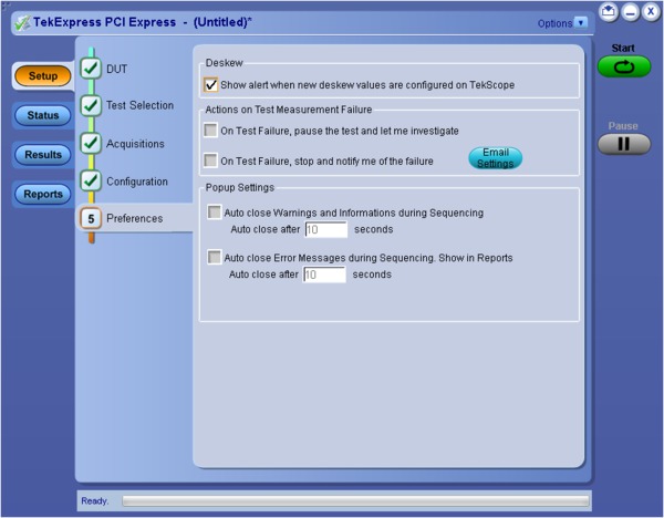
This makes use of the PCI-SIG's SigTest EXE to analyze the acquired waveforms. Thus makes the results of the analysis consistent with the SigTest post-capture analysis software used at PCI-SIG workshops for compliance testing.
The Option PCE3, Option PCE4 and Option PCE5 TekExpress automation software provides flexibility in selecting data rates, voltage swing, presets, and the tests to run. It also provides the option to de-embed the effects of the channel and the test fixtures and provide an accurate representation of the signal at the pins as required by the specification.
TekExpress uses Tektronix next generation PAM4 tool PAMJET for the measurement. During analysis, TekExpress will automatically set up the tool as per the specification, capture results, and report them to the user. PAMJET also allows expert users to configure the PAMJET tool to test the DUT in non-specification settings for debugging purposes.
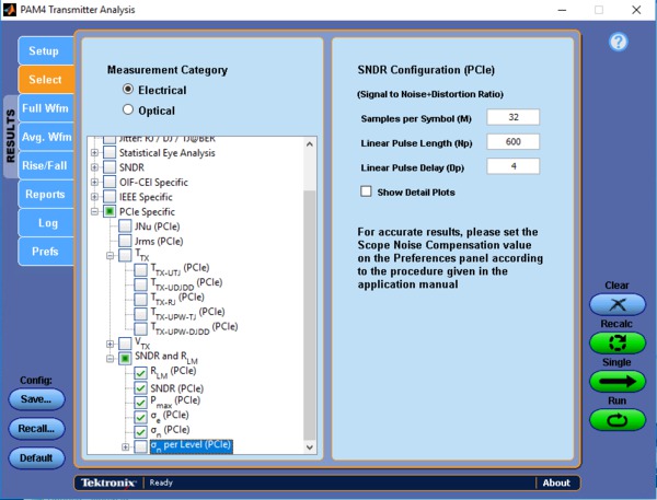
PAMJET introduces the Signal to Noise Distortion Ratio (SNDR) measurements with measurement methodology updated to support the latest PCI Express 6.0 Base Specification. Support for instrument noise compensation is integrated to improve measurement accuracy.
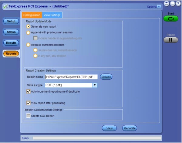
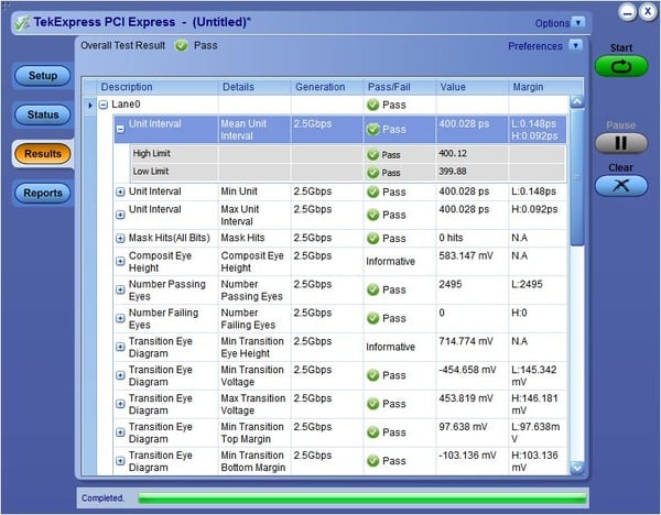
All the analysis results are compiled in a PDF/HTML/CSV formatted report that can include pass/fail summary, eye diagrams, setup configuration, and user comments. The contents of the report can be customized to include information of interest such as append results and custom report generation based on test name/pass fail/equalization.
Reference Clock Testing with TekExpress
Reference Clock testing has moved from optional to required for many designs due to the jitter limit decrease driven by the highest data rates supported by the PCI-SIG standards. Additionally, with the removal of dual-port (data and clock Tx testing) for Gen5 systems, compliance is required on the reference clock. The TekExpress PCIe solution has now integrated the SkyWorks Clock Jitter Tool to allow an automated hassle-free Reference Clock testing. Once the user connects the Reference Clock output to the oscilloscope, the TekExpress PCIe software will acquire the signal, invoke the SkyWorks Clock Jitter Tool, and provide Reference Clock test results from Gen1 to Gen5. Instrument noise compensations is supported with the Skyworks Clock Jitter Tool.
Switch Matrix automation
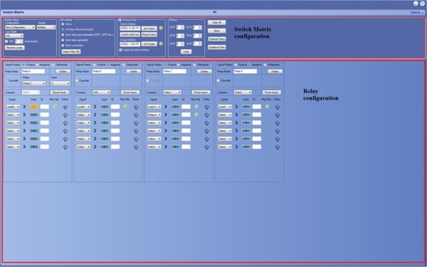
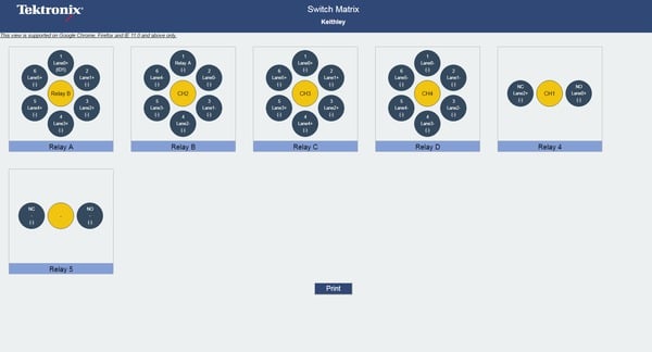
Switch Matrix application allows to configure and setup automated multi-lane testing using RF switch. The solution allows you to map each of the several transmitter signals and forward the selected input either to another relay or to the oscilloscope channel. Option SWX-PCE supports x12 and x16 lanes using Keithley and Gigatronics switches respectively, and enhances throughput and automated test speed.
Debug and validation
If a DUT or Add-In card fails any portion of the compliance test, the application includes a DPOJET-based debug and analysis tool kit customized for debug and validation of PCI Express interfaces.
The new jitter measurements introduced with PCIe Gen3 and Gen 4 provide separate limits for data dependent (DDJ) and uncorrelated deterministic jitter (UDJDD). It is important to separate DDJ (which can be compensated with transmitter and receiver equalization) and UDJDD (which can be caused by effects such as crosstalk and power supply noise).
Apart from the above Jitter measurements, Pulse Width Jitter (PWJ) is a new measurement that addresses the increased channel loss at 8 to 16 Gb/s. The purpose of the PWJ measurement is to ensure that lone bits meet minimum pulse width requirements. All new jitter measurements implement Q-scale extrapolation as defined in the base specification. The Tektronix Option PCE3, Option PCE4, and Option PCE5 provide the complete set of PCI Express 3.0, 4.0, and 5.0 Base Spec jitter measurements enabling silicon designers to verify that their silicon meets the base specification requirements.
Furthermore, the base specification requirements are defined at the pins of the transmitter. Before the measurements are computed the test channel must be de-embedded. De-embed filters can be easily created using the Tektronix Option SDLA64 Serial Data Link Analysis software and then quickly entered into the Option PCE3 and Option PCE4 base specification measurement setup and saved for future use. In addition to jitter, Option PCE3 and Option PCE4 also provide voltage, package loss, and transmitter equalization measurements.
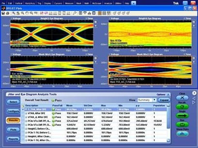
Option PCE3 and Option PCE4 leverage the channel modeling and receiver equalization functionality of the Tektronix Option SDLA64 software to support CEM measurements. Unlike other solutions, Option PCE3 and Option PCE4 provide full visibility to the signal as it has been modified to embed the compliance channel and provide receiver equalization. Eye diagrams and measurements can be set up to visually see the results of channel embedding, CTLE application, and DFE. For example, when determining the optimal Rx Equalization settings (CTLE setting and DFE tap value) the resulting eye diagrams and measurements show the effects of post processing on the acquired signal. Compliance measurements can then be taken on the waveform.



PAMJET for GEN6 Base Measurements
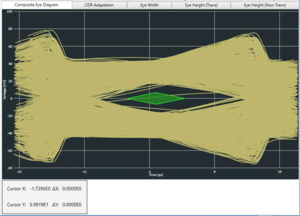
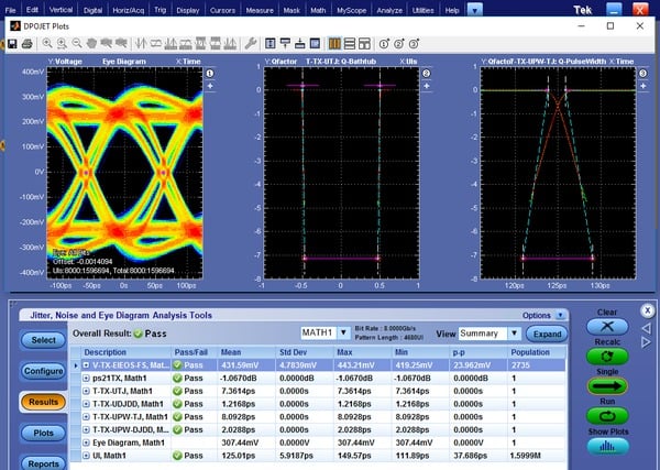
Tektronix has created a next generation PAM4 tool named PAMJET, which is used for Gen6 Base measurement. This PAMJET tool can configure the measurement and can perform Bessel Thompson filtering, configure Gen6 clock recovery, configure CTLE, and report the results. These built-in functions are specifically designed to aid Gen6 Base testing.
DPOJET based Reference Clock measurements
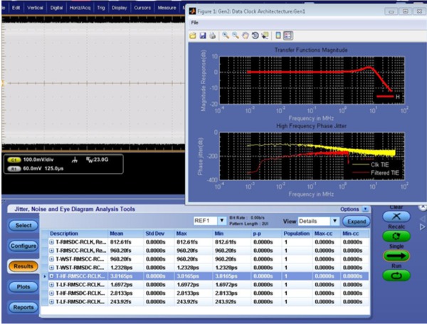
The Tektronix DPOJET based RefClock measurements provide a reliable way to implement the Reference clock specifications described in the PCI Express Base Specification Rev 1.0 for Gen1, Gen2, Gen3, Gen4 and Gen5.
Comprehensive programmatic interface
You can use Standard Commands for Programmable Instruments (SCPI) to communicate with the TekExpress application. The Online Help document of TekExpress application describes the steps for TCPIP socket configuration and TekVISA configuration to execute the SCPI commands.
PCI Express Decoder for Gen 1 - 4 (Option SR-PCIe)
Decode and Display of PCIe data in a protocol-aware view with the characters and names that are familiar from the standard such as the ordered sets: SKP, Electrical Idle, and EIEOS. A time correlated event table view with waveform allows for quickly searching through events of interest simultaneously. All decoding features support PCIe generations 1 - 4. The PCIe trigger is easily configured through Bus Setup under the oscilloscope's Vertical menu with a variety of user-adjustable settings. The PCIe data stream is integrated with serial bus trigger and search for PCIe gen 1 and 2 allows for triggering on information of interest.


Comprehensive measurements for PCIe validation, debug, and precompliance
Tektronix Option PCE3, Option PCE4 and Option PCE5 provide measurements that span multiple test points and versions of the PCIe specification. All PCIe specifications, test points, and measurements supported are listed in the following sections.
| Test method | Spec revision | PCI Express specification title | Test points defined |
|---|---|---|---|
| Rev 1.1 | Rev 1.1 | Base Specification | Transmitter and Receiver |
| Rev 1.1 | CEM Specification | System and Add-in Card Reference Clock | |
| Rev 1.0 | Express Module Specification | Transmitter Path and System Board | |
| Rev 1.0 | PCMCIA Express Card Standard | Host System Transmitter Express Card Transmitter | |
| Ver. 3.0 Rev 1.1 | Mobile PCI Express Module (MXM) Electromechanical Specification | PCI Express | |
| Rev 2.0 | Rev 1.0 | External Cabling Specification | Transmitter and Receiver Path |
| Rev 2.0 | Base Specification | Transmitter and Receiver Mobile Low-power Transmitter | |
| Rev 2.0 | CEM Specification | System and Add-in Card (3.5 and 6 dB de-emphasis) | |
| Ver. 3.0 Rev 1.1 | Mobile PCI Express Module (MXM) Electromechanical Specification | PCI Express | |
| Rev 3.0 | Rev 1.0 | Base Specification | Transmitter |
| Rev 1.0 | CEM Specification | System and Add-in Card | |
| Rev 3.0 | Test Specification | System and Add-in Card | |
| Rev 4.0 | Rev 1.0 | CEM Specification | System and Add-in Card |
| Rev 5.0 | Rev 1.0 | Base Specification | Transmitter |
| Rev 0.5 | CEM Specification | Transmitter | |
| Rev 6.0 | Rev 1.0 | Base Specification | Transmitter |
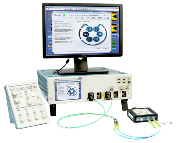
SignalConnect™ software and TCS70902 Calibration Source

Specifications
All specifications apply to all models unless noted otherwise.
Supported Reference clock measurements
- Supported Reference clock measurements
Generation Architecture Measurements Limits PCIe 1.1 Common clock T-CC- RCLK Specified T-WST-CC- RCLK Specified Independent RefClock IR2.5GBPS Specified PCIe 2.1 Common clock T-RMSCC-RCLK-5GBPS Specified T-WST-RMSCC-RCLK-5GBPS Specified Independent RefClock IR5GBPS Specified PCIe 3.1 Common clock T-RMSCC-RCLK Specified T-WST-RMSCC-RCLK Specified Independent RefClock IR8GBPS Specified PCIe 4.0 Common clock PCIE4_T-RMSCC-REFCLK Specified PCIE4_T-WST-RMSCC-REFCLK Specified Independent RefClock IR16GBPS Specified PCIe 5.0 Common clock PCIE5_T_RMSCC-REFCLK Specified PCIE5_T-WST-RMSCC-REFclk Specified Independent RefClock IR32GBPS Specified
Supported AC reference clock measurements
- AC reference clock specifications 1
Generation Specifications Measurements Symbol Common across all generations AC reference clock specifications Cycle to Cycle jitter CC_JITTER Differential Input High Voltage V_IH Differential Input Low Voltage V_IL Duty Cycle Duty Cycle Absolute Max input voltage Vmax Absolute Min input voltage Vmin Absolute Period (including Jitter and Spread Spectrum modulation) Period Abs Falling Edge Rate Falling-Edge-Rate Rising Edge Rate Rising-Edge-Rate Average Clock Period Accuracy Avg Prd Accur Rising edge rate (REFCLK+) to falling edge rate (REFCLK-) matching Rise fall Match Absolute crossing point voltage VCROSS SSC SlewRate SSC SlewRate
Supported base specification measurements
- Supported PCI Express 4.0 Base Transmitter measurements
Parameter DPOJET measurement 8.0 GT/s, Rev 3.0 16.0 GT/s, Rev 1.0 Full Swing Tx voltage with noTxEq V-TX-FS-NO-EQ Specified Specified Reduced Swing Tx voltage with noTxEq V-TX-RS-NO-EQ Specified Specified Min swing during EIEOS for full swing V-TX-EIEOS-FS Specified Specified Min swing during EIEOS for reduced swing V-TX-EIEOS-RS Specified Specified Pseudo package loss Root device ps21TXRootdevice Specified Specified Pseudo package loss AIC device ps21TXAICdevice Specified Specified Tx uncorrelated total Jitter T-TX-UTJ Specified Specified Tx uncorrelated deterministic jitter T-TX-UDJDD Specified Specified Data dependent jitter T-TX-DDJ Specified Specified Total uncorrelated PWJ T-TX-UPW-TJ Specified Specified Deterministic DjDD uncorrelated PWJ T-TX-UPW-DJDD Specified Specified Maximum Boost voltage ratio for full swing V-TX-FS-BOOST Specified Specified Maximum Boost voltage ratio for reduced swing V-TX-RS-BOOST Specified Specified Tx DC peak-peak common mode voltage VTX_DC_CM Specified NA Absolute Delta of DC Common Mode Voltage between D+ and D- VTX_CM_DC_LINE_DELTA Specified NA Electrical Idle Differential Peak Output Voltage VTX_IDLE_DIFF_AC_p Specified NA DC Electrical Idle Differential Output Voltage VTX_IDLE_DIFF_DC Specified NA
- Supported PCI Express 5.0 Base Transmitter measurements
Parameter DPOJET measurement 32.0 GT/s, Rev 5.0 Tx uncorrelated total Jitter T-TX-UTJ 6.25 ps (max) Tx uncorrelated deterministic Jitter T-TX-UDJDD 3.125 ps (max) Data dependent Jitter T-TX-DDJ NA Total uncorrelated PWJ T-TX-UPW-TJ 6.25 ps (max) Total Random Jitter (informative) T-TX-RJ 0.23-0.45 ps rms Deterministic DjDD uncorrelated PWJ T-TX- UPW-DJDD 2.5 ps (max) RMS RefClk jitter for common RefClk architecture T-RMSCC-RCLK 0.25 ps (max) IR RefClk jitter IR32GBPS NA Pseudo Package Loss ps21Tx (max) 8.5dB Boost ratio VTX-BOOST 8.0 (min) dB EIEOS VTX-EIEOS 250 mV TX Differential Peak to Peak VTX-DIFF-PP 800 mV (max) 1300mV Unit Interval UI 31.246875 (min) 31.253125 (max)
- Differential transmitter (Tx) output measurements
Parameter Symbol(s) 2.5 GT/s Rev 1.1/2.0 5 GT/s Rev 2.0 Clock Recovery NA Specified Specified Unit Interval UI Specified Specified Differential Peak-to-Peak Tx Voltage Swing VTX-DIFF-P-P
VTX-SWING
VTX-EYE-FULL
Specified Specified Low-power Differential Peak-to-Peak Tx Voltage Swing VTX-SWING-LOW
VTX-EYE-HALF
Specified Specified De-emphasized Output Voltage Ratio VTX-DE-RATIO Not Specified Specified Instantaneous Lane Pulse Width TMIN-PULSE Not Specified Specified Transmitter Eye including All Jitter Sources TTX-EYE
TTX-EYE-TJ
Specified Specified Maximum Time between the Jitter Median and Maximum Deviation from the Median TTX-EYEMEDIAN-to-MAXJITTER Specified Specified Deterministic Jitter TTX-DJ-DD Not Specified Specified Tx RMS Jitter <1.5 MHz TTX-LF-RMS Not Specified Specified D+/D– Tx Output Rise/Fall Time TTX-RISE
TTX-FALL
Specified Specified Tx Rise/Fall Mismatch TRF-MISMATCH Not Specified Specified AC Peak-to-Peak Common Mode Output Voltage VTX-CM-AC-PP Not Specified Specified AC Peak Common Mode Output Voltage VTX-CM-AC-P Specified Specified Absolute Delta of DC Common Mode Voltage between D+ and D– VTX-CM-DC-LINE-DELTA Specified Specified
Supported CEM specification measurements
- Add-in Card 8 GT/s transmitter path compliance measurements
Parameter Symbol Transition Eye Voltage PCIe V-TXA Nontransition Eye Voltage PCIe V-TXA-d Eye Width PCIe T-TXA
- Add-in Card transmitter path compliance measurements
Parameter Symbol(s) 2.5 Gt/s Rev 1.1/2.0 5 GT/s Rev 2.0 Clock Recovery NA Specified Specified Unit Interval UI Specified Specified Eye Height of Transition Bits VTXA Specified Specified Eye Height of Nontransition Bits VTXA_d Specified Specified Eye Width with Sample Size of 106 UI TTXA in Rev 1.1 Specified Not Specified Jitter Eye Opening at BER 10–12 TTXA in Rev 2.0 Specified Specified Maximum Median-Max Jitter Outlier with Sample Size of 106 UI JTXA-MEDIAN-to-MAX-JITTER Specified Not Specified Total Jitter at BER 10–12 TJ at BER 10–12 Not Specified Specified Deterministic Jitter at BER 10–12 Max DJ Not Specified Specified
- System board transmitter path measurements
Parameter Symbol(s) 2.5 GT/s Rev 1.1/2.0 5 GT/s Rev 2.0 Clock Recovery NA Specified Specified Unit Interval UI Specified Specified Eye Height of Transition Bits VTXS Specified Specified Eye Height of Nontransition Bits VTXS_d Specified Specified Eye Width with Sample Size of 106 UI TTXS in Rev 1.1 Specified Not Specified Jitter Eye Opening at BER 10–12 TTXS in Rev 2.0 Specified Specified Maximum Median-Max Jitter Outlier with Sample Size of 106 UI JTXA-MEDIAN-to-MAX-JITTER Specified Not Specified Total Jitter at BER 10–12 TJ at BER 10–12 Not Specified Specified Deterministic Jitter at BER 10–12 Max DJ Not Specified Specified
- Reference clock measurements
Parameter Symbol 2.5 Gt/s Rev 1.1/2.0 Reference Clock Phase Jitter at BER 10–6 NA Specified
PCI ExpressModule™ measurements
- ExpressModule Add-in Card transmitter path measurements
Parameter Symbol Rev 1.0 Clock Recovery NA Specified Unit Interval UI Specified Eye Height of Transition Bits VTXA Specified Eye Height of Nontransition Bits VTXA_d Specified Eye Width with Sample Size of 106 UI TTXAin Rev 1.1 Specified Jitter Eye Opening at BER 10–12 NA Specified Maximum Median-Max Jitter Outlier with Sample Size of 106 UI JTXA-MEDIAN-to-MAX-JITTER Specified
- ExpressModule system board transmitter path measurements
Parameter Symbol Gen1 Rev 1.0 Clock Recovery NA Specified Unit Interval UI Specified Eye Height of Transition Bits VTXS Specified Eye Height of Nontransition Bits VTXS_d Specified Eye Width with Sample Size of 106 UI TTXS Specified Jitter Eye Opening at BER 10–12 NA Specified Maximum Median-Max Jitter Outlier with Sample Size of 106 UI JTXA-MEDIAN-to-MAX-JITTER Specified
PCI Express external cabling measurements
- External cabling transmitter path measurements
Parameter Symbol Rev 1.0 Clock Recovery NA Specified Unit Interval UI Specified Eye Height of Transition Bits VTXA Specified Eye Height of Nontransition Bits VTXA_d Specified Jitter Eye Opening at BER 10–12 TrxA at BER 10–12 Specified Eye Width with Sample Size of 106 UI TrxA at 106 Samples Specified
PCMCIA ExpressCard™ measurements
- ExpressCard - Module transmitter path measurements
Parameter Symbol Release 1.0 Clock Recovery NA Specified Unit Interval UI Specified Eye Height of Transition Bits VTXA Specified Eye Height of Nontransition Bits VTXA_d Specified Eye Width across any 250 UIs TTXA Specified
ExpressCard-Host sys trans path
- ExpressCard™ - Host system transmitter path measurements
Parameter Symbol Release 1.0 Clock Recovery NA Specified Unit Interval UI Specified Eye Height of Transition Bits VtxS Specified Eye Height of Nontransition Bits VtxS_d Specified Eye Width across any 250 UIs TTxS Specified
MXM measurements
- PCI Express measurements2
Parameter Symbol Release 1.1 Eye Height of Transition Bits VTXS Specified Eye Height of Nontransition Bits VTXS_d Specified Width at BER TTXS Specified Deterministic Jitter DJ Specified Total Jitter TJ Specified
Ordering information
- PCE33
- PCI Express Gen1/2/3 TekExpress Compliance/Debug Automation with DPOJet Measurements Software
- New instrument orders
- Option PCE3
- Product upgrades
- DPO-UP Option PCE3
- Floating licenses
- DPOFL-PCE3
- PCE44
- PCI Express Gen4 TekExpress Compliance/Debug Automation with DPOJet Measurements Software
- Requires PCE3 option to support PCI Express Gen1/2/3 TekExpress Compliance/Debug Automation with DPOJet Measurements Software
For CEM System/Host Test 5
- New instrument orders
- Option PCE4
- Product upgrades
- DPO-UP Option PCE4
- Floating licenses
- DPOFL-PCE4
- PCE5
- TekExpress PCIe Tx Compliance Solution, supports PCIe Gen5 (requires Opt. DJA)
- New instrument orders
- Option PCE5
- Product upgrades
- DPO-UP Option PCE5
- Floating licenses
- DPOFL-PCE5
- PCE6
- TekExpress PCIe Tx Compliance Solution, supports PCIe Gen6 (requires Opt. DJA and PAMPCIE6)
- New instrument orders
- Option PCE6
- Product upgrades
- DPO-UP Option PCE6
- Floating licenses
- DPOFL-PCE6
- SWX-PCE6
- Switch configurator for PCIe Gen 1/2/3 (please note the RF Switch will not support PCIe Gen4 Tx testing)
- New instrument orders
- Option SWX-PCE
- Floating licenses
- DPOFL-SWX-PCE
Recommended DPO/MSO70000 Series Oscilloscopes
- 2.5 Gb/s (PCI Express 1.0/1.1)
- DPO/MSO70000 Series (6 GHz or higher bandwidth models required for compliance testing)
- 5.0 Gb/s (PCI Express 2.0)
- DPO/MSO70000 Series (12.5 GHz or higher bandwidth models)
- 8.0 Gb/s (PCI Express 3.0)
- DPO/MSO70000 Series (12.5 GHz or higher bandwidth models)
- 16.0 Gb/s (PCI Express 4.0)
- DPO/MSO70000 Series (25 GHz or higher bandwidth models)
- 32.0 Gb/s (PCI Express 5.0)
- DPS77004SX Series (50 GHz or higher bandwidth models), DPO/MSO70000 Series (33 GHz or higher bandwidth models for Gen5 CEM testing)
- 64.0 Gb/s (PCI Express 6.0)
- DPS77004SX Series (50 GHz or higher bandwidth models)
- Support for DPO/MSO70000 SX Series oscilloscopes
- Supported DPO70000 Series configurations
Model Description Option
PCE3
Option
PCE4
Option
PCE5
Option
PCE6
DPO71604C 16 GHz DPO; 2 Ch, 100 GS/s or 4 Ch, 50 GS/s ✓ DPO72004C 20 GHz DPO; 2 Ch, 100 GS/s or 4 Ch, 50 GS/s ✓ DSA71604C 16 GHz DSA; 2 Ch, 100 GS/s or 4 Ch, 50 GS/s ✓ DSA72004C 20 GHz DSA; 2 Ch, 100 GS/s or 4 Ch, 50 GS/s ✓ MSO71604C 16 GHz MSO; 2 Ch, 100 GS/s or 4 Ch, 50 GS/s ✓ MSO72004C 20 GHz MSO; 2 Ch, 100 GS/s or 4 Ch, 50 GS/s ✓ DPO72504D 25 GHz DPO; 2 Ch, 100 GS/s or 4 Ch, 50 GS/s ✓ ✓ DPO73304D 33 GHz DPO; 2 Ch, 100 GS/s or 4 Ch, 50 GS/s ✓ ✓ ✓ DSA72504D 25 GHz DSA; 2 Ch, 100 GS/s or 4 Ch, 50 GS/s ✓ ✓ DSA73304D 33 GHz DSA; 2 Ch, 100 GS/s or 4 Ch, 50 GS/s ✓ ✓ ✓ DPO72304DX 23 GHz DPO; 2 Ch, 100 GS/s or 4 Ch, 50 GS/s ✓ DPO72504DX 25 GHz DPO; 2 Ch, 100 GS/s or 4 Ch, 50 GS/s ✓ ✓ DPO73304DX 33 GHz DPO; 2 Ch, 100 GS/s or 4 Ch, 50 GS/s ✓ ✓ ✓ MSO72304DX 23 GHz MSO; 2 Ch, 100 GS/s or 4 Ch, 50 GS/s ✓ MSO72504DX 23 GHz MSO; 2 Ch, 100 GS/s or 4 Ch, 50 GS/s ✓ ✓ MSO73304DX 33 GHz MSO; 2 Ch, 100 GS/s or 4 Ch, 50 GS/s ✓ ✓ ✓ DPO77002SX 70 GHz ATI; 1 Ch, 70 GHz, 200 GS/s or 2 Ch, 33 GHz, 100 GS/s ✓ ✓ ✓ DPS77004SX 70 GHz ATI System; 2 Ch: 70 GHz: 200 GS/s or 4 Ch: 33 GHz: 100 GS/s ✓ ✓ ✓ ✓ DPO75902SX 59 GHz ATI; 1 Ch, 59 GHz, 200 GS/s or 2 Ch, 33 GHz, 100 GS/s ✓ ✓ ✓ DPS75904SX 59 GHz ATI System; 2 Ch: 59 GHz: 200 GS/s or 4 Ch: 33 GHz: 100 GS/s ✓ ✓ ✓ ✓ DPO75002SX 50 GHz ATI; 1 Ch, 50 GHz, 200 GS/s or 2 Ch, 33 GHz, 100 GS/s ✓ ✓ ✓ DPS75004SX 50 GHz ATI System; 2 Ch: 50 GHz: 200 GS/s or 4 Ch: 33 GHz: 100 GS/s ✓ ✓ ✓ ✓ DPO73304SX 33 GHz DPO; 2 Ch, 33 GHz, 100 GS/s or 4 Ch, 23 GHz, 50 GS/s ✓ ✓ ✓ DPS73308SX 33 GHz DPO System; 4 Ch: 33 GHz: 100 GS/s or 4 Ch: 23 GHz: 50 GS/s ✓ ✓ ✓ DPO72304SX 23 GHz DPO; 4 Ch: 23 GHz: 50 GS/s or 2 Ch: 23 GHz: 100 GS/s ✓ DPO71604SX 16GHz DPO; 4 Ch: 16GHz: 50GS/s or 2 Ch: 16 GHz: 100 GS/s ✓ DPO71304SX 13GHz DPO; 4 Ch: 13GHz: 50GS/s or 2 Ch: 13 GHz: 100 GS/s ✓
Accessories
Recommended accessories
- P75xx, P76xx, and P77xx Series (TriMode™ Differential Probes)
P7513, P7513A, P7516, P7520A, P7625, P7630, P7633, P7713, P7716, P7720 with respective tips
PCI Express Speed Minimum oscilloscope bandwidth TCA-SMA
(Max 18 GHz)
TCA-292D
(Max 33 GHz)
P7500
(Max 20 GHz)
P7700
(Max 20 GHz)
P7600
(Max 33 GHz)
2.5 GT/s 6 GHz ✓ ✓ ✓ ✓ ✓ 5.0 GT/s 12.5 GHz ✓ ✓ ✓ ✓ ✓ 8.0 GT/s 12.5 GHz ✓ ✓ ✓ ✓ ✓ 16.0 GT/s 25 GHz ✓ ✓ 32.0 GT/s BASE 50 GHz 32.0 GT/s CEM 33 GHz ✓ ✓ 100 MHz RefClk 5 GHz ✓ ✓ ✓ ✓ ✓ 64.0 GT/s BASE 50 GHz - Option SDLA64
- Serial Data Link Analysis Visualizer 7
- Option SR-PCIe
- Bus decode support for PCI Express serial busses 8
- Option PAMPCIE6
- Used for Gen6 Base
Recommended for automated DUT control
- RF Switch
- Keithley System S46T RF Microwave Switch for X12 PCIe
Gigatronics RF Switch 26 GHz (8902-L-48TS26) for x16 PCIe
- Tektronix AFG3252
- Arbitrary Function Generator
- Tektronix AFG3252C
- Arbitrary Function Generator
- AWG5002B/C
- Arbitrary Waveform Generator
- AWG5012B/C
- Arbitrary Waveform Generator
- AWG5014B/C
- Arbitrary Waveform Generator
- AWG7082B/C
- Arbitrary Waveform Generator
- AWG7122B/C
- Arbitrary Function Generator
- AWG70001A
- Arbitrary Waveform Generator
- AWG70002A
- Arbitrary Waveform Generator
- AFG31252
- Arbitrary Function Generator
- AFG31251
- Arbitrary Function Generator
- AFG3252C
- Arbitrary Function Generator
- GRL PCIE34 Controller for automatic test pattern toggling and DUT power cycle (for Add-In-Card)
Part number : GRL-PCIE34-P1
Contact GRL at for support and to request for a quote.
Recommended test fixtures, cables, and tools
| Description | Image |
|---|---|
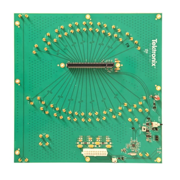
Description PCI Express 5.0 System Board (Tektronix NON-COMPLIANCE) Tektronix PN TF-PCIE5-CEM-X1 or TF-PCIE5-CEM-X16 Specifications
|  |
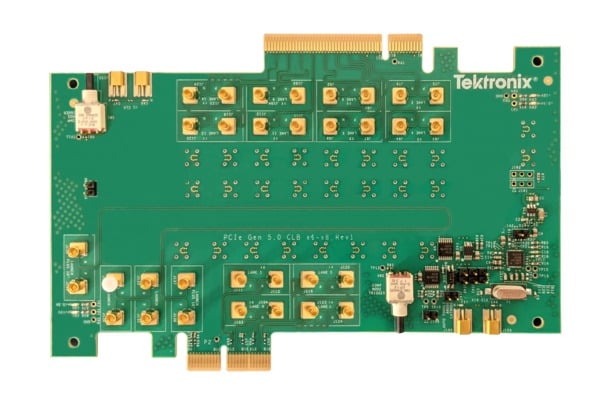
Description PCI Express 5.0 Add-in Card Board (Tektronix NON-COMPLIANCE) Tektronix PN TF-PCIE5-CEM-X1 or TF-PCIE5-CEM-X16 Specifications
|  |
Description PCI Express 5.0 Variable ISI Board (Tektronix NON-COMPLIANCE) Tektronix PN TF-PCIE5-CEM-X1 or TF-PCIE5-CEM-X16 Specifications
|  |
| Description: [PCI-SIG] PCIe 4.0 Preliminary CEM Fixture Kit PN: PCIe-CLB-X1X16, PCIe-CLB-X4X8, PCIe-CBB-MAIN, and PCIe-VAR-ISI The PCIe 4.0 CEM Beta fixtures require a VNA based characterization to determine the appropriate Insertion Loss for performing the 16 GT/s Tx Signal Quality Test and the 16 GT/s Rx Link Equalization Test. This characterization will not be performed by the PCI-SIG, but must be performed by the end user after the fixtures are delivered. Quantity: 1 | |
| Description: PCI Express Compliance Base Board (CBB) test fixture, revision 3.0. For testing PCI Express add-in cards, x1/x4/x8/x16 PCIe connectors on PCIe devices/add-in cards.
Vendor: PCI-SIG https://www.pcisig.com/specifications/order_form Vendor PN: CBB3 Tektronix PN: Only available from PCI-SIG Quantity: 1 |  |
| Description: PCI Express Compliance Load Board (CLB3) test fixture, revision 3.0. For testing PCI Express Platforms, x1 and x16 PCIe connectors on PCIe systems/mother boards. Vendor: PCI-SIG https://www.pcisig.com/specifications/order_form Vendor PN: x1/x16 CLB3 Tektronix PN: Only available from PCI-SIG Quantity: 1 | 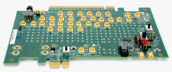 |
| Description: PCI Express Compliance Load Board (CLB3), Revision 3.0. For testing PCI Express Platforms, x4 and x8 PCIe connectors on PCIe systems/mother boards. Vendor: PCI-SIG https://www.pcisig.com/specifications/order_form Vendor PN: x4/x8 CLB3 Tektronix PN: Only available from PCI-SIG Quantity: 1 |  |
| Description: PCI Express Compliance Load Board (U.2 CLB3) test fixture, revision 3.0. For testing PCI Express Platforms, x1 and x4 PCIe connectors on PCIe devices/add-in cards. Vendor: PCI-SIG https://www.pcisig.com/specifications/order_form Vendor PN: U.2 CLB3 Tektronix PN: Only available from PCI-SIG Quantity: 1 Note: U.2 was formally known as SFF-8639. | 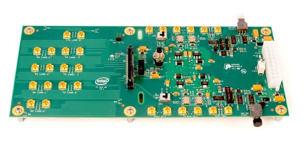 |
| Description: PCI Express Compliance Load Board (U.2 CLB3), Revision 3.0. For testing PCI Express Platforms, x1 and x4 PCIe connectors on PCIe systems/mother boards. Vendor: PCI-SIG https://www.pcisig.com/specifications/order_form Vendor PN: U.2 CLB3 Tektronix PN: Only available from PCI-SIG Quantity: 1 Note: U.2 was formally known as SFF-8639. |  |
| Description: Any ATX PC power supply Vendor: Tektronix recommends "PC Power and Cooling 750 W Silencer MK III Series" or similar. Quantity: 1 |  |
| Description: SMP terminator, 50 Ω, limited detent.
Vendor: Fairview Microwave http://www.fairviewmicrowave.com/rf-load-0.25-watts-26.5-ghz-smp-female-st2645-p.aspx Vendor PN: ST2645 Tektronix PN: 131-9399-xx Quantity needed per PCIe DUT link width:
|  |
| Description: SMA Female to BNC Male adapter.
Vendor: Tektronix Tektronix PN: 015-0572-xx Quantity: 2 |  |
| Description: DC Block, SMA, 26`GHz
Vendor: Tektronix Tektronix PN: PSPL5500A, PSPL5501A, or PSPL5508 Quantity: 2 Note: This is an optional accessory and not shown in any of connection diagrams, but can be used if DC offset is encountered in any signal path. |  |
| Description: USB2.0 Cable, Type A Male to Type B Male, 6 foot
Vendor: Tektronix Tektronix PN: 174-6053-xx Quantity: 1 |  |
| Description: SMA-to-SMA, H+S SF104E Phase Kit (#84077556), Straight, 1`m, 1.5 ps phase-matched.
Vendor: Tektronix Tektronix PN: PMCABLE1M Quantity: 1 cable pair per lane |  |
| Description: SMA-to-SMP right-angle cable pair, 102 mm, 1 ps phase-matched.
Tektronix PN: 174-6657-xx Quantity: 1 cable pair Note: Applicable only for Gen3 |  |
| Description: SMA-to-SMP right-angle cable pair, 1 m, 1 ps phase-matched (one for AFG to Rx Lane0, one for 100 MHz RefClk for Ch3+4 for System Testing)
Tektronix PN: 174-6659-xx Quantity: 1 cable pair |  |
| Description: SMP to SMP right-angle cable pair, 305 mm, 2.5 ps phase-matched set.
Tektronix PN: 174-6658-xx Quantity: 1 cable pair |  |
| Description Cables Tektronix PN TF-PCIE5-CEM-X1 or TF-PCIE5-CEM-X16 Specifications
| |
| Description: SMA torque wrench, 8.0 in-lbs.
Vendor: Fairview Microwave http://www.fairviewmicrowave.com/sma-fixed-torque-wrench-click-st-sma3-p.aspx Vendor PN: ST-SMA3 Tektronix PN: 003-1940-xx Quantity: 1 |  |
| Description: SMP right-angle cable extraction tool.
Vendor: Fairview Microwave http://www.fairviewmicrowave.com/undefined-mmtl2682-p.aspx Vendor PN: MMTL2682 Tektronix PN: 003-1941-xx Quantity: 1 |  |
| Description: SMP terminator installation/extraction tool.
Vendor: Fairview Microwave http://www.fairviewmicrowave.com/undefined-mmtl4991-p.aspx Vendor PN: MMTL4991 Tektronix PN: 003-1939-xx Quantity: 1 |  |
Additional information
PCI Express receiver testing
Tektronix also offers a complete PCI Express receiver testing solution for Gen5 and Gen4 that includes stressed pattern generation as required by PCI-SIG test specifications and support for automated calibration and receiver tests. Automated DUT loopback control simplifies the testing process and reduces the time to test results.
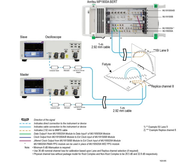
Salient features of the Receiver automation software with Tektronix DPO70000SX Series Real-Time Scopes and Anritsu MP1900A BERT are as follows:
- Wizard-based user interface for each step of calibration and test
- Efficient and quick calibration
- Insertion Loss computation powered by Seasim Statistical Simulation Tool
- Tx Link Equalization/Rx Link Equalization
- Jitter Tolerance
- Latest industry tool support (SigTest and Seasim)
- Comprehensive Calibration and test reports
- Automation for PCI Express PLL Bandwidth and Peaking tests (including SJ calibration) for Gen 3/4/5


