Свяжитесь с нами
Живой чат с представителями Tektronix. С 9:00 до 17:00 CET
Позвоните нам
С 9:00 до 17:00 CET
Загрузить
Загрузить руководства, технические описания, программное обеспечение и т. д.:
Обратная связь
5 Series MSO Specifications and Performance Verification Manual
This document contains the specifications and performance verification procedures for MSO54, MSO56, MSO58, and MSO58LP instruments.
Это руководство относится к следующему:
MSO56, MSO58, MSO58LP
- Тип руководства: Проверка рабочих характеристик
- Номер по каталогу: 077130607
- Дата выпуска:
By downloading, you agree to the terms and conditions of the Manuals Download Agreement.
Manuals Download Agreement
ATTENTION: please read the following terms and conditions carefully before downloading any documents from this website. By downloading manuals from Tektronix' website, you agree to the following terms and conditions:
Manuals for Products That Are Currently Supported:
Tektronix hereby grants permission and license to owners of Tektronix instruments to download and reproduce the manuals on this website for their own internal or personal use. Manuals for currently supported products may not be reproduced for distribution to others unless specifically authorized in writing by Tektronix, Inc.
A Tektronix manual may have been revised to reflect changes made to the product during its manufacturing life. Thus, different versions of a manual may exist for any given product. Care should be taken to ensure that one obtains the proper manual version for a specific product serial number.
Manuals for Products That Are No Longer Supported:
Tektronix cannot provide manuals for measurement products that are no longer eligible for long term support. Tektronix hereby grants permission and license for others to reproduce and distribute copies of any Tektronix measurement product manual, including user manuals, operator's manuals, service manuals, and the like, that (a) have a Tektronix Part Number and (b) are for a measurement product that is no longer supported by Tektronix.
A Tektronix manual may be revised to reflect changes made to the product during its manufacturing life. Thus, different versions of a manual may exist for any given product. Care should be taken to ensure that one obtains the proper manual version for a specific product serial number.
This permission and license does not apply to any manual or other publication that is still available from Tektronix, or to any manual or other publication for a video production product or a color printer product.
Disclaimer:
Tektronix does not warrant the accuracy or completeness of the information, text, graphics, schematics, parts lists, or other material contained within any measurement product manual or other publication that is not supplied by Tektronix or that is produced or distributed in accordance with the permission and license set forth above.
Tektronix may make changes to the content of this website or to its products at any time without notice.
Limitation of Liability:
TEKTRONIX SHALL NOT BE LIABLE FOR ANY DAMAGES WHATSOEVER (INCLUDING, WITHOUT LIMITATION, ANY CONSEQUENTIAL OR INCIDENTAL DAMAGES, DAMAGES FOR LOSS OF PROFITS, BUSINESS INTERRUPTION, OR FOR INFRINGEMENT OF INTELLECTUAL PROPERTY) ARISING OUT OF THE USE OF ANY MEASUREMENT PRODUCT MANUAL OR OTHER PUBLICATION PRODUCED OR DISTRIBUTED IN ACCORDANCE WITH THE PERMISSION AND LICENSE SET FORTH ABOVE.
Read Online
SPECIFICATIONS
- Analog channel input and vertical specification
- Timebase system
- Trigger system
- Serial Trigger specifications
- Digital acquisition system
- Digital volt meter (DVM)
- Trigger frequency counter
- Arbitrary Function Generator system
- Display system (MSO54, MSO56, MSO58)
- Processor system
- Input/Output port specifications
- Data storage specifications
- Power supply system
- Safety characteristics
- Environmental specifications
- Mechanical specifications
PERFORMANCE VERIFICATION PROCEDURES
- Test record
- Input Impedance test record
- DC Balance test record
- DC Gain Accuracy test record
- DC Offset Accuracy test record
- Analog Bandwidth test record
- Random Noise, sample acquisition mode test record
- Random Noise, High Res mode test record
- Long term sample rate through AFG DC offset accuracy test records
- Performance tests
- Prerequisites
- Self test
- Check input impedance
- Check DC balance
- Check DC gain accuracy
- Check DC offset accuracy
- Check analog bandwidth
- Check random noise, sample acquisition mode
- Check random noise, High Res mode
- Check long term sample rate
- Check delta time measurement accuracy
- Check digital threshold accuracy
- Check DVM voltage accuracy (DC)
- Check DVM voltage accuracy (AC)
- Check trigger frequency accuracy and maximum input frequency
- Check AFG sine and ramp frequency accuracy
- Check AFG square and pulse frequency accuracy
- Check AFG signal amplitude accuracy
- Check AFG DC offset accuracy
Important safety information
This manual contains information and warnings that must be followed by the user for safe operation and to keep the product in a safe condition.
General safety summary
Use the product only as specified. Review the following safety precautions to avoid injury and prevent damage to this product or any products connected to it. Carefully read all instructions. Retain these instructions for future reference.
This product shall be used in accordance with local and national codes.
For correct and safe operation of the product, it is essential that you follow generally accepted safety procedures in addition to the safety precautions specified in this manual.
The product is designed to be used by trained personnel only.
Only qualified personnel who are aware of the hazards involved should remove the cover for repair, maintenance, or adjustment.
Before use, always check the product with a known source to be sure it is operating correctly.
This product is not intended for detection of hazardous voltages.
Use personal protective equipment to prevent shock and arc blast injury where hazardous live conductors are exposed.
To avoid fire or personal injury
Use proper power cord
Use only the power cord specified for this product and certified for the country of use. Do not use the provided power cord for other products.
Ground the product
This product is grounded through the grounding conductor of the power cord. To avoid electric shock, the grounding conductor must be connected to earth ground. Before making connections to the input or output terminals of the product, ensure that the product is properly grounded. Do not disable the power cord grounding connection.
Power disconnect
The power cord disconnects the product from the power source. See instructions for the location. Do not position the equipment so that it is difficult to operate the power cord; it must remain accessible to the user at all times to allow for quick disconnection if needed.
Connect and disconnect properly
Do not connect or disconnect probes or test leads while they are connected to a voltage source.
Use only insulated voltage probes, test leads, and adapters supplied with the product, or indicated by Tektronix to be suitable for the product.
Observe all terminal ratings
To avoid fire or shock hazard, observe all rating and markings on the product. Consult the product manual for further ratings information before making connections to the product.
Do not exceed the Measurement Category (CAT) rating and voltage or current rating of the lowest rated individual component of a product, probe, or accessory. Use caution when using 1:1 test leads because the probe tip voltage is directly transmitted to the product.
Do not apply a potential to any terminal, including the common terminal, that exceeds the maximum rating of that terminal.
Do not operate without covers
Do not operate this product with covers or panels removed, or with the case open. Hazardous voltage exposure is possible.
Avoid exposed circuitry
Do not touch exposed connections and components when power is present.
Do not operate with suspected failures
If you suspect that there is damage to this product, have it inspected by qualified service personnel.
Disable the product if it is damaged. Do not use the product if it is damaged or operates incorrectly. If in doubt about safety of the product, turn it off and disconnect the power cord. Clearly mark the product to prevent its further operation.
Before use, inspect voltage probes, test leads, and accessories for mechanical damage and replace when damaged. Do not use probes or test leads if they are damaged, if there is exposed metal, or if a wear indicator shows.
Examine the exterior of the product before you use it. Look for cracks or missing pieces.
Use only specified replacement parts.
Do not operate in wet/damp conditions
Be aware that condensation may occur if a unit is moved from a cold to a warm environment.
Do not operate in an explosive atmosphere
Keep product surfaces clean and dry
Remove the input signals before you clean the product.
Provide proper ventilation
Refer to the installation instructions in the manual for details on installing the product so it has proper ventilation.
Slots and openings are provided for ventilation and should never be covered or otherwise obstructed. Do not push objects into any of the openings.
Provide a safe working environment
Always place the product in a location convenient for viewing the display and indicators.
Avoid improper or prolonged use of keyboards, pointers, and button pads. Improper or prolonged keyboard or pointer use may result in serious injury.
Be sure your work area meets applicable ergonomic standards. Consult with an ergonomics professional to avoid stress injuries.
Use care when lifting and carrying the product. This product is provided with a handle or handles for lifting and carrying.
 | WARNING:The product is heavy. To reduce the risk of personal injury or damage to the device get help when lifting or carrying the product. |
Use only the Tektronix rackmount hardware specified for this product.
Probes and test leads
Before connecting probes or test leads, connect the power cord from the power connector to a properly grounded power outlet.
Keep fingers behind the protective barrier, protective finger guard, or tactile indicator on the probes. Remove all probes, test leads and accessories that are not in use.
Use only correct Measurement Category (CAT), voltage, temperature, altitude, and amperage rated probes, test leads, and adapters for any measurement.
Terms in this manual and on the product
These terms may appear in this manual:
| WARNING:Warning statements identify conditions or practices that could result in injury or loss of life. |
| CAUTION:Caution statements identify conditions or practices that could result in damage to this product or other property. |
These terms may appear on the product:
- DANGER indicates an injury hazard immediately accessible as you read the marking.
- WARNING indicates an injury hazard not immediately accessible as you read the marking.
- CAUTION indicates a hazard to property including the product.
Symbols on the product
 | When this symbol is marked on the product, be sure to consult the manual to find out the nature of the potential hazards and any actions which have to be taken to avoid them. (This symbol may also be used to refer the user to ratings in the manual.) |
The following symbols(s) may appear on the product.
 CAUTION: Refer to Manual |  Protective Ground (Earth) Terminal |  Earth Terminal |  Chassis Ground |  Standby |
Specifications
This chapter contains specifications for the instrument. All specifications are typical unless noted as guaranteed. Typical specifications are provided for your convenience but are not guaranteed. Specifications that are marked with the ✔ symbol are guaranteed and checked in Performance Verification.
- The instrument must have been calibrated in an ambient temperature between 18 °C and 28 °C (64 °F and 82 °F).
- The instrument must be operating within the environmental limits described in these specifications.
- The instrument must be powered from a source that meets the specifications.
- The instrument must have been operating continuously for at least 20 minutes within the specified operating temperature range.
- You must perform the Signal path compensation procedure after the warmup period. See the Signal path compensation procedure for how to perform signal path compensation. If the ambient temperature changes more than 5 °C (9 °F), repeat the procedure.
Warranted specifications describe guaranteed performance with tolerance limits or certain type-tested requirements.
Analog channel input and vertical specification
- Number of input channels
- MSO54: 4 BNC
- Input coupling
- DC, AC
- Input resistance selection
- 1 MΩ or 50 Ω
- ✓Input impedance 1 MΩ DC coupled
-
1 MΩ ±1%
- Input capacitance 1 MΩ DC coupled, typical
- 14.5 pF ±1.5 pF, 2 GHz model
- ✓Input impedance 50 Ω, DC coupled
- 50 Ω ±1% (VSWR ≤1.5:1, typical)
- Maximum input voltage, 1 MΩ
- 300 VRMS at the BNC. Installation Category II
- Maximum input voltage, 50 Ohm
-
5 VRMS, with peaks ≤ ±20 V (DF ≤6.25%)
- DC balance
- ✓ 0.1 div with DC-50 Ω oscilloscope input impedance (50 Ω BNC terminated)
| Note: 500 µV/div is a 2X digital zoom of 1 mV/div. As such, it is guaranteed by testing the 1 mV/div setting. |
- Number of digitized bits
- 8 bits at 6.25 GS/s
- Sensitivity range, coarse
-
- 1 MΩ
- 500 µV/div to 10 V/div in a 1-2-5 sequence
- 50 Ω
- 500 µV/div to 1 V/div in a 1-2-5 sequence
- Sensitivity range, fine
-
Allows continuous adjustment from 1 mV/div to 10 V/div, 1 MΩ and from 1 mV/div to 1 V/div, 50 Ω
- 1 MΩ
- 500 µV/div to 10 V/div
- 50 Ω
- 500 µV/div to 1 V/div
- Sensitivity resolution, fine
- ≤1% of current setting
- ✓ DC gain accuracy
-
- 2 GHz model, Step Gain, 50 Ω
- ±1.2%, (±2.0% at 1 mV/div and 500 µV/div settings), de-rated at 0.100%/ °C above 30 °C
- 2 GHz model, Step Gain, 1 MΩ
- ±1.0%, (±2.0% at 1 mV/div and 500 µV/div settings), de-rated at 0.100%/ °C above 30 °C
- 1 GHz, 500 MHz, 350 MHz models, MSO58LP, Step Gain
- ±1.0%, (±2.0% at 1 mV/div and 500 µV/div settings), de-rated at 0.100%/ °C above 30 °C
- Variable gain
- ±1.5%, de-rated at 0.100%/ °C above 30 °C.
| Note: 500 µV/div is a 2X digital zoom of 1 mV/div. As such, it is guaranteed by testing the 1 mV/div setting. |
- Offset ranges, maximum
-
- 2 GHz models
-
Input signal cannot exceed maximum input voltage for the 50 Ω input path.
Volts/div Setting Maximum offset range, 50 Ω Input 500 µV/div - 50 mV/div ±1 V 51 mV/div - 99 mV/div ± (-10 * (Volts/div Setting) + 1.5 V) 100 mV/div - 500 mV/div ±10 V 501 mV/div - 1 V/div ± (-10 * (Volts/div Setting) + 15 V) Volts/div Setting Maximum offset range, 1 MΩ Input 500 µV/div - 63 mV/div ±1 V 64 mV/div - 999 mV/div ±10 V 1 V/div - 10 V/div ±100 V - ≤ 1 GHz models (including MSO58LP)
-
Input signal cannot exceed maximum input voltage for the 50 Ω input path.
Volts/div Setting Maximum offset range 50 Ω Input 1 MΩ Input 500 µV/div - 63 mV/div ±1 V ±1 V 64 mV/div - 999 mV/div ±10 V ±10 V 1 V/div - 10 V/div ±10 V ±100 V
| Note: 500 µV/div is a 2X digital zoom of 1 mV/div. As such, it is guaranteed by testing the 1 mV/div setting.
|
- Position range
- ±5 divisions
- ✓Offset accuracy
-
±(0.005 X | offset - position | + DC balance )
- Number of waveforms for average acquisition mode
- 2 to 10,240 Waveforms, default 16 waveforms
- DC voltage measurement accuracy, Average acquisition mode
-
Measurement Type DC Accuracy (In Volts) Average of ≥ 16 waveforms ±((DC Gain Accuracy) * |reading - (offset - position)| + Offset Accuracy + 0.1 * V/div setting) Delta volts between any two averages of ≥ 16 waveforms acquired with the same oscilloscope setup and ambient conditions ±(DC Gain Accuracy * |reading| + 0.05 div)
- DC voltage measurement accuracy, sample acquisition mode, typical
-
Measurement Type DC Accuracy (In Volts) Any Sample ±(DC Gain Accuracy * |reading - (offset - position)| + Offset Accuracy + 0.15 div + 0.6 mV) Delta Volts between any two samples acquired with the same oscilloscope setup and ambient conditions ±(DC Gain Accuracy * |reading| + 0.15 div + 1.2 mV)
- Bandwidth selections
- 50 Ω: 20 MHz, 250 MHz, and the full bandwidth value of your model
- MSO58LP Bandwidth selections
- 20 MHz, 250 MHz, and 1 GHz
- ✓Analog bandwidth 50 Ω DC coupled
-
- 2 GHz models
-
Volts/Div Setting Bandwidth 10 mV/div - 1 V/div DC - 2.00 GHz 5 mV/div - 9.98 mV/div DC - 1.50 GHz 2 mV/div - 4.98 mV/div DC - 350 MHz 1 mV/div - 1.99 mV/div DC - 175 MHz 500 µV/div - 995 µV/div DC - 175 MHz - 1 GHz models
-
Volts/Div Setting Bandwidth 1 mV/div - 1 V/div DC - 1.00 GHz 500 µV/div - 995 µV/div DC - 250 MHz - 500 MHz models
-
Volts/Div Setting Bandwidth 1 mV/div - 1 V/div DC - 500 MHz 500 µV/div - 995 µV/div DC - 250 MHz - 350 MHz models
-
Volts/Div Setting Bandwidth 1 mV/div - 1 V/div DC - 350 MHz 500 µV/div - 995 µV/div DC - 250 MHz
- Analog bandwidth, 1 MΩ, typical
-
- All model bandwidths except 350 MHz
-
Volts/Div Setting Bandwidth 1 mV/div - 10 V/div DC - 500 MHz 500 µV/div - 995 µV/div DC - 250 MHz - 350 MHz models
-
Volts/Div Setting Bandwidth 1 mV/div - 10 V/div DC - 350 MHz 500 µV/div - 995 µV/div DC - 250 MHz
- Analog bandwidth with TPP0500, TPP1000 probes, typical
- The limits are for ambient temperature of ≤30 °C and the bandwidth selection set to FULL. Reduce the upper bandwidth frequency by 1% for each °C above 30 °C.
Instrument Volts/Div Setting Bandwidth 2 GHz, 1 GHz 5 mV/div - 100 V/div DC - 1 GHz (TPP1000 Probe) 500 MHz 5 mV/div - 100 V/div DC - 500 MHz (TPP0500 Probe) 350 MHz 5 mV/div - 100 V/div DC - 350 MHz (TPP0500 Probe)
- Lower frequency limit, AC coupled, typical
-
<10 Hz when AC 1 MΩ coupled. The AC coupled lower frequency limits are reduced by a factor of 10 (<1 Hz) when 10X passive probes are used.
- Upper frequency limit, 250 MHz bandwidth limited, typical
-
250 MHz, ± 25%
- Upper frequency limit, 20 MHz bandwidth limited, typical
-
20 MHz, ± 20%
- Calculated rise time, typical
-
Model 50 Ω TPP0500 Probe TP1000 Probe Vertical 500 µV-1 V 5 mV-10 V 5 mV-10 V 2 GHz 225 ps 800 ps 400 ps 1 GHz 400 ps 800 ps 400 ps 500 MHz 800 ps 800 ps 800 ps 350 MHz 1.15 ns 1.15 ns 1.15 ns
- Peak Detect or Envelope mode pulse response, typical
-
Minimum pulse width is >640 ps (6.25 GS/s)
- Effective bits (ENOB), typical
- Typical effective bits for a 9-division p-p sine-wave input, 50 mV/div, 50 Ω
- 2 GHz models, Sample mode, 50 Ω
-
Bandwidth Input frequency 6.25 GS/s 2 GHz 10 MHz 6.20 2 GHz 600 MHz 6.20 250 MHz 10 MHz 7.30 250 MHz 200 MHz 7.30 20 MHz 10 MHz 7.60 - 2 GHz models, High Res mode, 50 Ω
-
Bandwidth Input frequency 6.25 GS/s 1 GHz 10 MHz 7.00 1 GHz 300 MHz 7.00 250 MHz 10 MHz 7.80 250 MHz 100 MHz 7.80 20 MHz 10 MHz 8.70 - 1 GHz, 500 MHz, 350 MHz models, Sample mode, 50 Ω
-
Bandwidth Input Frequency 6.25 GS/s 1 GHz 10 MHz 7.10 1 GHz 300 MHz 7.10 500 MHz 10 MHz 7.40 500 MHz 150 MHz 7.40 350 MHz 10 MHz 7.60 350 MHz 100 MHz 7.60 250 MHz 10 MHz 7.50 250 MHz 100 MHz 7.50 20 MHz 10 MHz 7.70 - 1 GHz, 500 MHz, 350 MHz models, High Res mode, 50 Ω
-
Bandwidth Input frequency 6.25 GS/s 1 GHz 10 MHz 7.60 1 GHz 300 MHz 7.50 500 MHz 10 MHz 7.90 500 MHz 150 MHz 7.80 350 MHz 10 MHz 8.20 350 MHz 100 MHz 8.20 250 MHz 10 MHz 8.10 250 MHz 100 MHz 8.10 20 MHz 10 MHz 8.90
- Random noise, sample acquisition mode
- Bandwidth at 1 mV/div is limited to 175 MHz in 50 Ω. Bandwidth at 2 mV/div is limited to 350 MHz in 50 Ω. Bandwidth at 5 mV/div is limited to 1.5 GHz in 50 Ω.
- Delay between analog channels, full bandwidth, typical
-
≤ 100 ps for any two channels with input impedance set to 50 Ω, DC coupling with equal Volts/div or above 10 mV/div
- Deskew range
-
-125 ns to +125 ns with a resolution of 40 ps
- Crosstalk (channel isolation), typical
-
≥ 200:1 up to the rated bandwidth for any two channels having equal Volts/div settings
- Overdrive recovery time, typical
-
- 50 Ω, no probe, 1 GHz bandwidth
-
Vertical scale 500% overdrive 5000% overdrive 5% 1% 0.2% 5% 1% 0.2% 1 mV/div <1 μs 2.0 ms 2.0 ms --- --- --- 10 mV/div <1 μs 3.0 ms 33 μs <1.2 μs <4.7 μs --- 100 mV/div <1 μs <1 μs 5.8 μs --- --- - 50 Ω, no probe, 2 GHz bandwidth
-
Vertical scale 500% overdrive 5000% overdrive 5% 1% 0.2% 5% 1% 0.2% 1 mV/div <1 μs 110 μs 2.0 ms --- --- --- 10 mV/div <1 μs <1 μs 2.0 ms <1 μs <1 μs --- 100 mV/div <1 μs <1 μs 2.3 ms --- --- - TPP1000 Probe
-
Vertical scale 500% overdrive 5000% overdrive 5% 1% 0.2% 5% 1% 0.2% 10 mV/div 20 μs 2.0 ms 2.0 ms 30 μs 50 μs 2.2 ms 20 mV/div 14 μs 2.0 ms 2.0 ms 30 μs 50 μs 110 μs 50 mV/div 12 μs 60 μs 2.0 ms --- --- --- 100 mV/div 12 μs 60 μs 2.0 ms --- --- ---
- Total probe power
-
TekVPI Compliant probe interfaces (8 per MSO58, 6 per MSO56, 4 per MSO54)
MSO58 and MSO56: 80 W maximum, (40 W maximum for channels 1 through 4, 40 W maximum for channels 5 through 8)
MSO54: 40 W maximum
- Probe power per channel
-
Voltage Max Amperage Voltage Tolerance 5 V 60 mA ±10% 12 V 2 A (20 W maximum software limit) ±10%
- TekVPI interconnect
-
All analog channel inputs on the front panel conform to the TEKVPI specification.
Timebase system
- Sample rate
-
Max HW Capability Number of Channels 6.25 GS/s 1- 8
- Interpolated waveform rate range
-
500 GS/sec, 250 GS/sec, 125 GS/sec, 62.5 GS/sec, 25 GS/sec, and 12.5 GS/sec
- Record length range
-
- Standard
- 1 kpoints to 125 Mpoints in single sample increments
- Standard
- 1 kpoints to 62.5 Mpoints in single sample increments
- Optional 5-RL-125M
- 125 Mpoints
- Seconds/Division range
-
Model 1 K 10 K 100 K 1 M 10 M 62.5 M 125 M MSO5X Standard 62.5 M 200 ps - 64 s 200 ps - 640 s 200 ps - 1000 s MSO5X Option 5-RL-125M 200 ps - 64 s 200 ps - 640 s 200 ps - 1000 s
- Maximum triggered acquisition rate, typical
-
Analog or digital channels: single channel [Analog or Digital 8-bit channel] on screen, measurements and math turned off. >40 wfm/sec
FastAcq Update Rate (analog only): >500 K/second with one channel active and >100 K/second with all eight active.
FastAcq Update Rate (analog and analog/digital): >400 K/second with two channels active and >100 K/second with all eight analog channels active.
Digital channel: >40/second with one channel (8-bits) active. There is no FastAcq for digital channels, but they do not slow down FastAcq for active analog channels.
- Aperture uncertainty
-
≤ 0.450 ps + (1 * 10-11 * Measurement Duration)RMS, for measurements having duration ≤ 100 ms
- ✓Timebase accuracy
-
±2.5 x 10⁻⁶ over any ≥1 ms time interval
Description Specification Factory Tolerance ±5.0 x10⁻⁷ At calibration, 23 °C ambient, over any ≥1 ms interval
Temperature stability ±5.0 x10⁻⁷ Tested at operating temperatures
Crystal aging ±1.5 x 10⁻⁶ Frequency tolerance change at 25 °C over a period of 1 year
- ✓Delta-time measurement accuracy, typical
-
The formula to calculate delta-time measurement accuracy (DTA) for a given instrument setting and input signal is given below (assumes insignificant signal content above Nyquist)
SR1 = Slew Rate (1st Edge) around 1st point in measurement
SR2 = Slew Rate (2nd Edge) around 2nd point in measurement
N = input-referred guaranteed noise limit. If Ntyp is what's specified, then N is computed by multiplying Ntyp by some scale factor (e.g., 1.5)
TBA = timebase accuracy or Reference Frequency Error +/-5 ppm
tp = delta-time measurement duration (sec)
The term under the square root sign is the stability and is due to TIE (Time Interval Error). The errors due to this term occur throughout a single-shot measurement. The second term is due to both the absolute center-frequency accuracy and the center-frequency stability of the timebase and varies between multiple single-shot measurements over the observation interval (the amount of time from the first single-shot measurement to the final single-shot measurement).Note:The formulas assume negligible errors due to measurement interpolation, and apply only when the interpolated sample rate is 25 GS/s or higher.

Trigger system
- Trigger bandwidth (edge, pulse, and logic), typical
-
2 GHz models, Edge 2 GHz 2 GHz models, Pulse and Logic 1 GHz 1 GHz models including MSO58LP 1 GHz 500 MHz models 500 MHz 350 MHz models 350 MHz
- Edge-type trigger sensitivity, DC coupled, typical
-
Table 1. 5 Series MSO Path Range Specification 1 MΩ path (all models) 0.5 mV/div to 0.99 mV/div 5 mV from DC to instrument bandwidth ≥ 1 mV/div The greater of 5 mV or 0.7 div from DC to lesser of 500 MHz or instrument BW, & 6 mV or 0.8 div from > 500 MHz to instrument bandwidth 50 Ω path, 1 GHz, 500 MHz, 350 MHz models The greater of 5.6 mV or 0.7 div from DC to the lesser of 500 MHz or instrument BW, & 7 mV or 0.8 div from > 500 MHz to instrument bandwidth 50 Ω path, 2 GHz models 0.5 mV/div to 0.99 mV/div 3.0 div from DC to instrument bandwidth 1 mV/div to 9.98 mV/div 1.5 divisions from DC to instrument bandwidth ≥ 10 mV/div < 1.0 division from DC to instrument bandwidth Line Fixed Table 2. MSO58LP Path Range Specification 1 MΩ path (all models) 0.5 mV/div to 0.99 mV/div 4.5 div from DC to instrument bandwidth ≥ 1 mV/div The greater of 5 mV or 0.7 div from DC to lesser of 500 MHz or instrument BW, & 6 mV or 0.8 div from > 500 MHz to instrument bandwidth 50 Ω path The greater of 5.6 mV or 0.7 div from DC to the lesser of 500 MHz or instrument BW, & 7 mV or 0.8 div from > 500 MHz to instrument bandwidth Line Fixed AUX Trigger in 200 mVPP, DC to 250 MHz
- Trigger jitter, typical
-
≤ 5 psRMS for sample mode and edge-type trigger
≤ 7 psRMS for edge-type trigger and FastAcq mode
≤ 40 psRMS for non edge-type trigger modes
≤ 200 psRMS for AUX trigger in, Sample acquisition mode, edge trigger (MSO58LP only)
≤ 220 psRMS for AUX trigger in, FastAcq acquisition mode, edge trigger (MSO58LP only)
- AUX In trigger skew between instruments, typical
-
±100 ps jitter on each instrument with 150 ps skew; ≤350 ps total between instruments.
Skew improves for sinusoidal input voltages ≥500 mV
- Edge-type trigger sensitivity, not DC coupled, typical
-
Trigger Coupling Typical Sensitivity NOISE REJ 2.5 times the DC Coupled limits HF REJ 1.0 times the DC Coupled limits from DC to 50 kHz. Attenuates signals above 50 kHz. LF REJ 1.5 times the DC Coupled limits for frequencies above 50 kHz. Attenuates signals below 50 kHz.
- Lowest frequency for successful operation of Set Level to 50% function, typical
- 45 Hz
- Logic-type, logic qualified trigger, or events-delay sensitivities, DC coupled, typical
- 2.0 divisions, at vertical settings ≥5 mV/div.
- Pulse-type runt trigger sensitivities, typical
- 2.0 division at vertical settings ≥5 mV/div.
- Pulse-type trigger width and glitch sensitivities, typical
- 2.0 divisions at vertical settings ≥5 mV/div.
- Logic-type triggering, minimum logic or rearm time, typical
- For Logic, time between channels refers to the length of time a logic state derived from more than one channel must exist to be recognized. For Events, the time is the minimum time between a main and delayed event that will be recognized if more than one channel is used.
- Minimum clock pulse widths for setup/hold time violation trigger, typical
- Active pulsewidth is the width of the clock pulse from its active edge (as defined in the Clock Edge menu item) to its inactive edge. Inactive pulsewidth is the width of the pulse from its inactive edge to its active edge.
- Setup/hold violation trigger, setup and hold time ranges, typical
-
Feature Min Max Setup Time 0 ns 20 s Hold Time 0 ns 20 s Setup + Hold Time 320 ps 22 s Input coupling on clock and data channels must be the same.
For Setup Time, positive numbers mean a data transition before the clock.
For Hold Time, positive numbers mean a data transition after the clock edge.
Setup + Hold Time is the algebraic sum of the Setup Time and the Hold Time programmed by the user.
- Pulse type trigger, minimum pulse, rearm time, transition time
-
Pulse class Minimum pulse width Minimum rearm time Runt 160 ps + trise 160 ps + trise Time-Qualified Runt 160 ps + trise 160 ps + trise Width 160 ps + trise 160 ps + trise Slew Rate (minimum transition time) 160 ps + trise 160 ps + trise For trigger class width, pulse width refers to the width of the pulse being measured. Rearm time refers to the time between pulses.
For trigger class runt, pulse width refers to the width of the pulse being measured. Rearm time refers to the time between pulses.
For trigger class slew rate, pulse width refers to the delta time being measured. Rearm time refers to the time it takes the signal to cross the two trigger thresholds again.
trise is rise time of the instrument.
Active pulsewidth is the width of the clock pulse from its active edge (as defined in the Clock Edge menu item) to its inactive edge
Inactive pulsewidth is the width of the pulse from its inactive edge to its active edge.
- Transition time trigger, delta time range
- 160 ps to 20 s.
- Time range for glitch, pulse width, timeout, time-qualified runt, or time-qualified window triggering
- 160 ps to 20 s.
- Time accuracy for pulse, glitch, timeout, or width triggering
-
Time Range Accuracy 1 ns to 500 ns ±(160 ps +Time Base Error * Setting). 520 ns to 1 s ±(160 ps +Time Base Error * Setting).
- B trigger after events, minimum pulse width and maximum event frequency, typical
- Minimum pulse width:
160 ps
+ trise
Maximum event frequency: Instrument bandwidth.
trise is rise time of the instrument.
- B trigger, minimum time between arm and trigger, typical
-
320 ps
For trigger after time, this is the time between the end of the time period and the B trigger event.
For trigger after events, this is the time between the last A trigger event and the first B trigger event.
- B trigger after time, time range
- 160 ps to 20 seconds
- B trigger after events, event range
- 1 to 65,471
- Trigger level ranges
-
Source Range Any Channel ±5 divs from center of screen Line Fixed at about 50% of line voltage Source Range Any Channel ±5 divs from center of screen Aux In Trigger ±5 V Line Fixed at about 50% of line voltage This specification applies to logic and pulse thresholds.
- Trigger level accuracy, DC coupled, typical
- For signals having rise and fall times ≥10 ns:
- Trigger holdoff range
- 0 ns to 10 seconds
Serial Trigger specifications
- Maximum serial trigger bits
- 128 bits
- Optional serial bus interface triggering
-
- I2C
-
Address Triggering: 7 & 10 bits of user-specified addresses supported
Data Trigger: 1 - 5 Bytes of user-specified data
Trigger on: Start, Repeated Start, Stop, Missing Ack, Data, Address, or Address & Data
Maximum Data Rate: 10 Mb/s
- SPI
-
Data Trigger: 1 - 16 Bytes of user-specified data
Trigger on: SS Active, Data
Maximum Data Rate: 20 Mb/s
- CAN
-
Data Trigger: 1 - 8 Bytes of user-specified data, including qualifiers of equal to (=), not equal to (≠), less than (<), greater than (>), less than or equal to (<=), greater than or equal to (>=)
Trigger on: Start of Frame, Type of Frame, Identifier, Data, Identifier & Data, End of Frame, Missing Ack, or Bit Stuffing Errors
Frame Type: Data, Remote, Error, Overload
Identifier: Standard (11 bit) and Extended (29 bit) identifiers
Maximum Data Rate: 1 Mb/s
- LIN
-
Identifier Trigger: 6 bits of user-specified data, equal to (=)
Data Trigger: 1 - 8 Bytes of user-specified data, including qualifiers of equal to (=), not equal to (≠), less than (<), greater than (>), less than or equal to (<=), greater than or equal to (>=), inside range, outside range
Error Trigger: Sync, Identifier Parity, Checksum
Trigger on: Sync, Identifier, Data, Identifier & Data, Wakeup Frame, Sleep Frame, or Error
Maximum Data Rate: 100 kb/s
- Flexray
-
Indicator Bits: Normal (01XX), Payload (11XX), Null (00XX), Sync (XX10), Startup (XX11)
Frame ID Trigger: 11 bits of user-specified data, including qualifiers of equal to (=), not equal to (≠), less than (<), greater than (>), less than or equal to (<=), greater than or equal to (>=)
Cycle Count Trigger: 6 bits of user-specified data , including qualifiers of equal to (=), not equal to (≠), less than (<), greater than (>), less than or equal to (<=), greater than or equal to (>=)
Header Fields Trigger: 40 bits of user-specified data comprising Indicator Bits, Identifier, Payload Length, Header CRC, and Cycle Count, equal to (=)
Data Trigger: 1 - 16 Bytes of user-specified data, with 0 to 253, or "don't care" bytes of data offset,including qualifiers of equal to (=), not equal to (≠), less than (<), greater than (>), less than or equal to (<=), greater than or equal to (>=), Inside Range, Outside Range
End Of Frame: User-chosen types Static, Dynamic (DTS), and All
Error Trigger: Header CRC, Trailer CRC, Null Frame-static, Null Frame-dynamic, Sync Frame, Startup frame (No Sync)
Trigger on: Start of Frame, Frame ID, Indicator Bits, Cycle Count, Header Fields, Data, Identifier & Data, End of Frame, or Error
Maximum Data Rate: 40 Mb/s
- Audio (I2S)
-
Data Trigger: 32 bits of user-specified data in a left word, right word, or either, including qualifiers of equal to (=), not equal to (≠), less than (<), greater than (>), less than or equal to (<=), greater than or equal to (>=), inside range, outside range
Trigger on: Word Select, Data
Maximum Data Rate: 12.5 Mb/s
Left Justified (LJ)
Data Trigger: 32 bits of user-specified data in a left word, right word, or either, including qualifiers of equal to (=), not equal to (≠), less than (<), greater than (>), less than or equal to (<=), greater than or equal to (>=), inside range, outside range
Trigger on: Word Select, Data
Maximum Data Rate: 12.5 Mb/s
Right Justified (RJ)
Data Trigger: 32 bits of user-specified data in a left word, right word, or either, including qualifiers of equal to (=), not equal to (≠), less than (<), greater than (>), less than or equal to (<=), greater than or equal to (>=), inside range, outside range
Trigger on: Word Select, Data
Maximum Data Rate: 12.5 Mb/s
TDM
Data Trigger: 32 bits of user-specified data in a channel 1-64, including qualifiers of equal to (=), not equal to (≠), less than (<), greater than (>), less than or equal to (<=), greater than or equal to (>=), inside range, outside range
Trigger on: Frame Sync, Data
Maximum Data Rate: 25 Mb/s
- RS232
-
Bit Rate: 50 bps - 10 Mbps
Data Bits: 7, 8, or 9
Parity: None, Odd, or Even
Trigger on: Start, End of Packet, Data, Parity Error
- MIL-STD-1553
-
Bit Rate: 1 Mb/s
Trigger on:
Sync
Word Type (Command, Status, Data)
Command Word (set RT Address (=, ≠, <, >, ≤, ≥, inside range, outside range), T/R, Sub-address/ Mode, Data Word Count/Mode Code, and Parity individually)
Status Word (set RT Address ((=, ≠, <, >, ≤, ≥, inside range, outside range), Message Error, Instrumentation, Service Request Bit, Broadcast Command Received, Busy, Subsystem Flag, Dynamic Bus Control Acceptance (DBCA), Terminal Flag, and Parity individually)
Data Word (user-specified 16-bit data value)
Error (Sync, Parity, Manchester, Non-contiguous data)
Idle Time (minimum time selectable from 4 μs to 100 μs; maximum time selectable from 12 μs to 100 μs; trigger on < minimum, > maximum, inside range, outside range)
For MIL-STD-1553, Trigger selection of Command Word will trigger on Command and ambiguous Command/Status words. Trigger selection of Status Word will trigger on Status and ambiguous Command/Status words
- USB
-
Data Rates Supported: High: 480 Mbs, Full: 12 Mbs, Low: 1.5Mbs
Trigger On: Sync, Reset, Suspend, Resume, End of Packet, Token Packet, Data Packet, Handshake Packet, Special Packet, Error
- Ethernet
-
Bit Rate: 10 BASE-T, 10 Mbps; 100 BASE-TX, 100 Mbps
Trigger On: Start of Frame, MAC Address, MAC Length/Type, IP Header, TCP Header, Client Data, End of Packet, Idle, FCS (CRC) Error, MAC Q-Tag control Information
Digital acquisition system
- Digital channel maximum sample rate
- 6.25 GS/s
- Transition detect (digital peak detect)
- Displayed data at sample rates less than 6.25 GS/s (decimated data), that contains multiple transitions between sample points will be displayed with a bright white colored edge.
- Digital-To-Analog trigger skew
- 1 ns
- Digital to digital skew
- 320 ps from bit 0 of any TekVPI channel to bit 0 of any TekVPI channel.
- Digital skew within a FlexChannel
- 160 ps within any TekVPI channel
Digital volt meter (DVM)
- Measurement types
-
DC, ACRMS+DC, ACRMS
- Voltage resolution
- 4 digits
- ✓ Voltage accuracy
-
- DC:
-
±((1.5% * |reading - offset - position|) + (0.5% * |(offset - position)|) + (0.1 * Volts/div))
De-rated at 0.100%/°C of |reading - offset - position| above 30 °C
Signal ± 5 divisions from screen center
- AC:
-
± 2% (40 Hz to 1 kHz) with no harmonic content outside 40 Hz to 1 kHz range
AC, typical: ± 2% (20 Hz to 10 kHz)
For AC measurements, the input channel vertical settings must allow the VPP input signal to cover between 4 and 10 divisions and must be fully visible on the screen
Trigger frequency counter
- Resolution
- 8-digits
- ✓Accuracy
-
±(1 count + time base accuracy * input frequency)
The signal must be at least 8 mVpp or 2 div, whichever is greater.
- ✓Maximum input frequency
- 10 Hz to maximum bandwidth of the analog channel
Arbitrary Function Generator system
- Function types
- Arbitrary, sine, square, pulse, ramp, triangle, DC level, Gaussian, Lorentz, exponential rise/fall, sin(x)/x, random noise, Haversine, Cardiac
- Amplitude range
- Values are peak-to-peak voltages
Waveform 50 Ω 1 MΩ Arbitrary 10 mV to 2.5 V 20 mV to 5 V Sine 10 mV to 2.5 V 20 mV to 5 V Square 10 mV to 2.5 V 20 mV to 5 V Pulse 10 mV to 2.5 V 20 mV to 5 V Ramp 10 mV to 2.5 V 20 mV to 5 V Triangle 10 mV to 2.5 V 20 mV to 5 V Gaussian 10 mV to 1.25 V 20 mV to 2.5 V Lorentz 10 mV to 1.2 V 20 mV to 2.4 V Exponential Rise 10 mV to 1.25 V 20 mV to 2.5 V Exponential Fall 10 mV to 1.25 V 20 mV to 2.5 V Sine(x)/x 10 mV to 1.5 V 20 mV to 3.0 V Random Noise 10 mV to 2.5 V 20 mV to 5 V Haversine 10 mV to 1.25 V 20 mV to 2.5 V Cardiac 10 mV to 2.5 V 20 mV to 5 V
- Maximum sample rate
- 250 MS/s
- Arbitrary function record length
- 128 K Samples
- Sine waveform
-
- Frequency range
- 0.1 Hz to 50 MHz
- Frequency setting resolution
- 0.1 Hz
- Frequency accuracy
-
130 ppm (frequency ≤ 10 kHz), 50 ppm (frequency > 10 kHz)
This is for Sine, Ramp, Square and Pulse waveforms only.
- Amplitude range
- 20 mVpp to 5 Vpp into Hi-Z; 10 mVpp to 2.5 Vpp into 50 Ω
- Amplitude flatness, typical
-
±0.5 dB at 1 kHz
±1.5 dB at 1 kHz for < 20 mVpp amplitudes
- Total harmonic distortion, typical
-
1% for amplitude ≥ 200 mVpp into 50 Ω load
2.5% for amplitude > 50 mV AND < 200 mVpp into 50 Ω load
This is for Sine wave only.
- Spurious free dynamic range, typical
-
40 dB (Vpp ≥ 0.1 V); 30 dB (Vpp ≥ 0.02 V), 50 Ω load
- Square and pulse waveform
-
- Frequency range
- 0.1 Hz to 25 MHz
- Frequency setting resolution
- 0.1 Hz
- Duty cycle range
-
10% - 90% or 10 ns minimum pulse, whichever is larger
Minimum pulse time applies to both on and off time, so maximum duty cycle will reduce at higher frequencies to maintain 10 ns off time
- Duty cycle resolution
- 0.1%
- Minimum pulse width, typical
- 10 ns. This is the minimum time for either on or off duration.
- Rise/Fall time, typical
- 5 ns, 10% - 90%
- Pulse width resolution
- 100 ps
- Overshoot, typical
- <
6% for signal steps greater than 100 mVpp
This applies to overshoot of the positive-going transition (+overshoot) and of the negative-going (-overshoot) transition
- Asymmetry, typical
- ±1% ±5 ns, at 50% duty cycle
- Jitter, typical
- < 60 ps TIERMS, ≥ 100 mVpp amplitude, 40%-60% duty cycle
- Cardiac maximum frequency
- 1 MHz
- Ramp and triangle waveform
-
- Frequency range
- 0.1 Hz to 500 kHz
- Frequency setting resolution
- 0.1 Hz
- Variable symmetry
- 0% - 100%
- Symmetry resolution
- 0.1%
- DC level range
-
±2.5 V into Hi-Z
±1.25 V into 50 Ω
- Gaussian pulse, Haversine, and Lorentz pulse
-
- Maximum frequency
- 5 MHz
- Exponential rise fall maximum frequency
- 5 MHz
- Sin(x)/x
-
- Maximum frequency
- 2 MHz
- Random noise amplitude range
-
20 mVpp to 5 Vpp into Hi-Z
10 mVpp to 2.5 Vpp into 50 Ω
For both isolated noise signal and additive noise signal.
- ✓Sine and ramp frequency accuracy
-
1.3 x 10⁻⁴ (frequency ≤10 kHz)
5.0 x 10⁻⁵ (frequency >10 kHz)
- ✓Square and pulse frequency accuracy
-
1.3 x 10⁻⁴ (frequency ≤10 KHz);
5.0 x 10⁻⁵ (frequency >10 KHz)
- Signal amplitude resolution
-
1 mV (Hi-Z)
500 μV (50 Ω)
- ✓Signal amplitude accuracy
- ±[ (1.5% of peak-to-peak amplitude setting) + (1.5% of absolute DC offset setting) + 1 mV ] (frequency = 1 kHz)
- DC offset range
-
±2.5 V into Hi-Z
±1.25 V into 50 Ω
- DC offset resolution
-
1 mV (Hi-Z)
500 μV (50 Ω)
- ✓DC offset accuracy
- ±[ (1.5% of absolute offset voltage setting) + 1 mV ]
Display system (MSO54, MSO56, MSO58)
- Display type
-
Display area - 13.55 inches (344.16 mm) (H) x 7.62 inches (193.59 mm) (V), 15.55 inches (395 mm) diagonal, 6-bit RGB color, (1920 X 1080) TFT liquid crystal display (LCD) with capacitive touch
- Display resolution
- 1,920 horizontal × 1,080 vertical pixels (High Definition)
- Luminance, typical
-
250 cd/m2, (Minimum: 200 cd/m2
)
Display luminance is specified for a new display set at full brightness.
- Color support
- 262K (6-bit RGB) colors.
Processor system
- Host processor
- Intel i5-4400E, 2.7 GHz, 64-bit, dual core processor
- Operating system
-
Default instrument: Closed Linux
Instrument with option 5-WIN installed: Microsoft Windows 10. Option 5-WIN is not available for MSO58LP instrument.
- Internal storage
- ≥ 80 GB. Form factor is an 80 mm m.2 card with a SATA-3 interface
- Solid State Drive (SSD) with Microsoft Windows 10 OS (option 5-WIN )
- ≥ 512 GB SSD. Form factor is a 2.5-inch SSD with a SATA-3 interface. This drive is customer installable and includes the Microsoft Windows 10 Enterprise IoT 2016 LTSB (64-bit) operating system
Input/Output port specifications
- Ethernet interface
- An 8-pin RJ-45 connector that supports 10/100/1000 Mb/s
- Video signal output
- A 15-pin, 3-row, D-sub VGA connector.
- DVI connector
-
A 29-pin DVI-D connector; connect to show the oscilloscope display on an external monitor or projector
Maximum supported resolution, Windows: 1920 x 1200 @ 60 Hz
Maximum supported resolution, Linux: 1920 x 1080 @ 60 Hz
Only a single TMDS link is provided
Analog VGA signaling is not provided
- DisplayPort connector
-
A 20-pin DisplayPort connector; connect to show the oscilloscope display on an external monitor or projector
Maximum supported resolution, Windows: 2560 x 1440 @ 60Hz
Maximum supported resolution, Linux: 1920 x 1080 @ 60 Hz
DP++ adapter: Maximum supported resolution: 2560 x1440 @ 60 Hz
- Simultaneous displays
- Up to 3 displays (including the internal display) with a maximum of 1 display per port.
- USB interface (Host, Device ports)
-
5 Series MSO Front panel USB Host ports: Two USB 2.0 Hi-Speed ports, one USB 3.0 SuperSpeed port
MSO58LP Front panel USB Host ports: One USB 2.0 Hi-Speed port, one USB 3.0 SuperSpeed port
All instruments, Rear panel USB Host ports: Two USB 2.0 Hi-Speed ports, two USB 3.0 SuperSpeed ports
All instruments, Rear panel USB Device port: One USB 3.0 SuperSpeed Device port providing USBTMC support
- Probe compensator signal output voltage and frequency, typical
-
Characteristic Value Output Voltage Default: 0-2.5 V amplitude Impedance 1 kΩ Frequency 1 kHz
- ✓Auxiliary output, AUX OUT, Trigger Out, Event, or Reference Clock Out
-
- Selectable output
-
Acquisition Trigger Out
Reference Clock Out
AFG Trigger Out
- Acquisition Trigger Out
- User selectable transition from HIGH to LOW, or LOW to HIGH, indicates the trigger occurred. The signal returns to its previous state after approximately 100 ns
- Acquisition trigger jitter
-
300 ps (peak-to-peak)
- Reference Clock Out
- Reference clock output tracks the acquisition system and can be referenced from either the internal clock reference or the external clock reference
- AFG Trigger Out
-
The output frequency is dependent on the frequency of the AFG signal as shown in the following table:
AFG signal frequency AFT trigger frequency ≤ 4.9 MHz Signal frequency > 4.9 MHz to 14.7 MHz Signal frequency / 3 > 14.7 MHz to 24.5 MHz Signal frequency / 5 > 24.5 MHz to 34.3 MHz Signal frequency / 7 > 34.3 MHz to 44.1 MHz Signal frequency / 9 > 44.1 MHz to 50 MHz Signal frequency / 11 - AUX OUT Output Voltage
-
Characteristic Limits Vout (HI) ≥ 2.5 V open circuit; ≥ 1.0 V into a 50 Ω load to ground Vout (LO) ≤ 0.7 V into a load of ≤ 4 mA; ≤0.25 V into a 50 Ω load to ground
- External reference input
-
- Nominal input frequency
-
10 MHz
- Frequency Variation Tolerance
-
9.99996 MHz to 10.00004 MHz (±4.0 x 10⁻⁶)
- Sensitivity, typical
-
Vin 1.5 Vp-p using a 50 Ω termination
- Maximum input signal
- 7 Vpp
- Impedance
-
1.2 K Ohms ±20% in parallel with 18 pf ±5 pf at 10 MHz
Data storage specifications
- Nonvolatile memory retention time, typical
- No time limit for front panel settings, saved waveforms, setups, product licensing, and calibration constants.
- Real-time clock
- A programmable clock providing time in years, months, days, hours, minutes, and seconds.
- Nonvolatile memory capacity
-
- Instrument S/N
-
A 2 kbit EEPROM on the main board that stores the instrument serial number, instrument start up count, total uptime and administration passwords.
- Companion CvP
- A pair of 16 Mbit flash memory devices that stores a portion of the Companion FPGA image data. One device serves as a backup for the other device.
- AFG S/N
- A 2 kbit EEPROM on the AFG riser card that stores a copy of the instrument serial number which is used to validate the AFG calibration.
- Front Panel ID
- A 64 kbit EEPROM on the LED board that stores the USB vendor ID and device ID for the internal front panel controller.
- BIOS
- A 128 Mbit flash memory device that stores the firmware image and device configuration for the host processor and chipset sub-processors. This includes the Basic Input Output System (BIOS), Management Engine (ME), Embedded Controller (EC) and Network Interface Controller (NIC). The Ethernet MAC address is stored in this device.
- CMOS Memory
- The host processor chipset includes an integrated memory device, powered by the real-time clock (RTC) battery, which stores BIOS configuration settings. A customer accessible switch disconnects the RTC battery from the chipset which clears the contents of the integrated CMOS memory device.
- Memory SPD
- Each SODIMM (memory module) contains a serial presence detect (SPD) memory device implemented using an unspecified memory technology. Each SPD device contains the parameter data specific to its memory module. All SPD devices are treated by the instrument as read only. The size of a given SPD is unspecified. The 4 channel instrument includes 4 SPD devices. The 6 channel and 8 channel instruments include 6 SPD devices.
- UCD9248
- The instrument includes 3 UCD9248 power supply controllers. Each controller contains an unspecified quantity of nonvolatile memory that stores various power supply configuration settings.
- PMU
- A power management unit (PMU) microcontroller is used to manage instrument power supplies and hardware initialization. The PMU includes 32 KB of nonvolatile memory for storage of its own binary executable and redundant storage of UCD9248 device settings.
- Analog Board Controller
-
A microcontroller is used to manage analog board operation. The PMU includes 64 KB of nonvolatile memory for storage of its own binary executable.
- Carrier FPGA
-
The carrier FPGA stores its own configuration in its own internal 0.33 Mbit nonvolatile memory. The carrier FPGA implements simple "glue logic" for the instrument.
- Mass storage device capacity
-
- Linux
- ≥ 250 GB. Form factor is a 2.5 inch SSD with a SATA-3 interface. Waveforms and setups are stored on the solid state drive. Provides storage for saved customer data and the Linux operating system.
- Windows (optional)
- ≥ 500 GB. Form factor is a 2.5 inch SSD with a SATA-3 interface. This drive is customer installable and provides storage for the Windows operating system option, and saved customer data.
Power supply system
- Power
-
- Power consumption
- 400 Watts maximum
- Source voltage
- 100 - 240 V ±10% (50 Hz to 60 Hz)
- Source frequency
- 50 Hz to 60 Hz ±10%, at 100 - 240 V ±10%
- Fuse Rating
- 12.5 A, 250 Vac
Safety characteristics
- Safety certification
-
US NRTL Listed - UL61010-1 and UL61010-2-030
Canadian Certification - CAN/CSA-C22.2 No. 61010.1 and CAN/CSA-C22.2 No 61010.2.030
EU Compliance - Low Voltage Directive 2014-35-EU and EN61010-1.
International Compliance - IEC 61010-1 and IEC61010-2-030
- Pollution degree
- Pollution degree 2, indoor, dry location use only
Environmental specifications
- Temperature
-
- Operating
- +0 °C to +50 °C (32 °F to 122 °F)
- Non-operating
- -20 °C to +60 °C (-4 °F to 140 °F)
- Humidity
-
- Operating
- 5% to 90% relative humidity (% RH) at up to +40 °C
- Non-operating
- 5% to 90% relative humidity (% RH) at up to +40 °C
- Altitude
-
- Operating
- Up to 3,000 meters (9,843 feet)
- Non-operating
- Up to 12,000 meters (39,370 feet)
- Random vibration
-
- Operating
- 0.31 GRMS, 5-500 Hz, 10 minutes per axis, 3 axes (30 minutes total)
- Non-operating
- 2.46 GRMS, 5-500 Hz, 10 minutes per axis, 3 axes (30 minutes total)
- Temperature
-
- Operating
- +0 °C to +50 °C (32 °F to 122 °F)
- Non-operating
-
-20 °C to +60 °C (-4 °F to 140 °F)
- Humidity
-
- Operating
-
5% to 90% relative humidity (% RH) at up to +40 °C
5% to 55% RH above +40 °C up to +50 °C, noncondensing, and as limited by a maximum wet-bulb temperature of +39 °C
- Non-operating
-
5% to 90% relative humidity (% RH) at up to +40 °C
5% to 39% RH above +40 °C up to +50 °C, noncondensing, and as limited by a maximum wet-bulb temperature of +39 °C
- Altitude
-
- Operating
- Up to 3,000 meters (9,843 feet)
- Non-operating
- Up to 12,000 meters (39,370 feet)
- Random vibration, MSO58LP
-
- Operating
- 0.31 GRMS, 5-500 Hz, 10 minutes per axis, 3 axes (30 minutes total)
- Non-operating
- 2.46 GRMS, 5-500 Hz, 10 minutes per axis, 3 axes (30 minutes total)
Mechanical specifications
- Dimensions, 5 Series MSO
-
Height: 12.2 in (309 mm), feet folded in, handle to back
Height: 14.6 in (371 mm) feet folded in, handle up
Width: 17.9 in (454 mm) from handle hub to handle hub
Depth: 8.0 in (205 mm) from back of feet to front of knobs, handle up
Depth: 11.7 in (297.2 mm) feet folded in, handle to the back
- Dimensions, MSO58LP
-
Height: 3.44 in (87.3 mm)
Width: 17.01 in (432 mm)
Depth: 23.85 in (605.7 mm)
Fits rack depths from 24 inches to 32 inches
- Weight, 5 Series MSO
-
MSO54 1 GHz, 500 MHz, 350 MHz models: 22.7 lbs (10.3 kg)
MSO54 2 GHz models: 23.6 lbs (10.7 kg)
MSO56 1 GHz, 500 MHz, 350 MHz models: 23.5 lbs (10.7 kg)
MSO56 2 GHz models: 24.3 lbs (11 kg)
MSO58 1 GHz, 500 MHz, 350 MHz models: 23.8 lbs (10.8 kg)
MSO58 2 GHz models: 24.7 lbs (11.2 kg)
Front cover without pouch: 1.9 lbs (0.86 kg)
Front cover with pouch: 3.1 lbs (1.4 kg)
- Weight, MSO58LP
-
25.5 lbs (11.6 kg)
- Cooling , 5 Series MSO
- The clearance requirement for adequate cooling is 2.0 in (50.8 mm) on the right side of the instrument (when viewed from the front) and on the rear of the instrument
- Cooling, MSO58LP
- The clearance requirement for adequate cooling is 2.0 in (50.8 mm) on the left and right sides of the instrument (when viewed from the front). Air flows through the instrument from left to right
Performance verification procedures
This chapter contains performance verification procedures for the specifications marked with the ✔ symbol. The following equipment, or a suitable equivalent, is required to complete these procedures.
The performance verification procedures verify the performance of your instrument. They do not adjust your instrument. If your instrument fails any of the performance verification tests, repeat the failing test, verifying that the test equipment and settings are correct. If the instrument continues to fail a test, contact Tektronix Customer Support for assistance.
These procedures cover all 5 Series MSO instruments. Completion of the performance verification procedure does not update the instrument time and date.
Print the test records on the following pages and use them to record the performance test results for your oscilloscope. Disregard checks and test records that do not apply to the specific model you are testing.
The following table lists the required equipment. You might need additional cables and adapters, depending on the actual test equipment you use.
| Required equipment | Minimum requirements | Examples |
|---|---|---|
| DC voltage source | 3 mV to 4 V, ±0.1% accuracy | Fluke 9500B Oscilloscope Calibrator with a 9530 Output Module |
| Leveled sine wave generator | 50 kHz to 2 GHz, ±4% amplitude accuracy | |
| Time mark generator | 80 ms period, ±1.0 x 10⁻⁶ accuracy, rise time <50 ns | |
| Logic probe | Low capacitance digital probe, 8 channels. | TLP058 probe |
| BNC-to-0.1 inch pin adapter to connect the logic probe to the signal source. | BNC-to-0.1 inch pin adapter; female BNC to 2x16 .01 inch pin headers. | Tektronix adapter part number 878-1429-00; to connect the Fluke 9500B to the TLP058 probe. |
| Digital multimeter (DMM) | 0.1% accuracy or better | Tektronix DMM4020 |
| One 50 Ω terminator | Impedance 50 Ω; connectors: female BNC input, male BNC output | Tektronix part number 011-0049-02 |
| One 50 Ω BNC cable | Male-to-male connectors | Tektronix part number 012-0057-01 |
| Optical mouse | USB, PS2 | Tektronix part number 119-7054-00 |
| RF vector signal generator | Maximum bandwidth of instrument | Tektronix TSG4100A |
Test record
Instrument information, self test record
| Model | Serial # | Procedure performed by | Date |
|---|---|---|---|
|
|
|
|
|
| Test | Passed | Failed |
|---|---|---|
| Self Test |
|
|
Input Impedance test record
| Input Impedance | ||||
|---|---|---|---|---|
| Performance checks | Vertical scale | Low limit | Test result | High limit |
| All models | ||||
| Channel 1 Input Impedance, 1 MΩ | 100 mV/div | 990 kΩ | 1.01 MΩ | |
| Channel 1 Input Impedance, 50 Ω | 10 mV/div | 49.5 Ω | 50.5 Ω | |
| 100 mV/div | 49.5 Ω | 50.5 Ω | ||
| Channel 2 Input Impedance, 1 MΩ | 100 mV/div | 990 kΩ | 1.01 MΩ | |
| Channel 2 Input Impedance, 50 Ω | 10 mV/div | 49.5 Ω | 50.5 Ω | |
| 100 mV/div | 49.5 Ω | 50.5 Ω | ||
| Channel 3 Input Impedance, 1 MΩ | 100 mV/div | 990 kΩ | 1.01 MΩ | |
| Channel 3 Input Impedance, 50 Ω | 10 mV/div | 49.5 Ω | 50.5 Ω | |
| 100 mV/div | 49.5 Ω | 50.5 Ω | ||
| Channel 4 Input Impedance, 1 MΩ | 100 mV/div | 990 kΩ | 1.01 MΩ | |
| Channel 4, Input Impedance, 50 Ω | 10 mV/div | 49.5 Ω | 50.5 Ω | |
| 100 mV/div | 49.5 Ω | 50.5 Ω | ||
| MSO56, MSO58, MSO58LP models | ||||
| Channel 5 Input Impedance, 1 MΩ | 100 mV/div | 990 kΩ | 1.01 MΩ | |
| Channel 5 Input Impedance, 50 Ω | 10 mV/div | 49.5 Ω | 50.5 Ω | |
| 100 mV/div | 49.5 Ω | 50.5 Ω | ||
| Channel 6 Input Impedance, 1 MΩ | 100 mV/div | 990 kΩ | 1.01 MΩ | |
| Channel 6 Input Impedance, 50 Ω | 10 mV/div | 49.5 Ω | 50.5 Ω | |
| 100 mV/div | 49.5 Ω | 50.5 Ω | ||
| MSO58, MSO58LP models | ||||
| Channel 7 Input Impedance, 1 MΩ | 100 mV/div | 990 kΩ | 1.01 MΩ | |
| Channel 7 Input Impedance, 50 Ω | 10 mV/div | 49.5 Ω | 50.5 Ω | |
| 100 mV/div | 49.5 Ω | 50.5 Ω | ||
| Channel 8 Input Impedance, 1 MΩ | 100 mV/div | 990 kΩ | 1.01 MΩ | |
| Channel 8, Input Impedance, 50 Ω | 10 mV/div | 49.5 Ω | 50.5 Ω | |
| 100 mV/div | 49.5 Ω | 50.5 Ω | ||
DC Balance test record
| DC Balance | ||||
|---|---|---|---|---|
| Performance checks | Vertical scale | Low limit | Test result | High limit |
| All models | ||||
| Channel 1 DC Balance, 50 Ω, 20 MHz BW | 1 mV/div | -0.2 mV | 0.2 mV | |
| 2 mV/div | -0.2 mV | 0.2 mV | ||
| 5 mV/div | -0.5 mV | 0.5 mV | ||
| 10 mV/div | -1 mV | 1 mV | ||
| 20 mV/div | -2 mV | 2 mV | ||
| 49.8 mV/div | -4.98 mV | 4.98 mV | ||
| 50 mV/div | -5 mV | 5 mV | ||
| 100 mV/div | -10 mV | 10 mV | ||
| 200 mV/div | -20 mV | 20 mV | ||
| 500 mV/div | -50 mV | 50 mV | ||
| 1 V/div | -100 mV | 100 mV | ||
| Channel 1 DC Balance, 1 MΩ, 20 MHz BW | 1 mV/div | -0.2 mV | 0.2 mV | |
| 2 mV/div | -0.4 mV | 0.4 mV | ||
| 5 mV/div | -1 mV | 1 mV | ||
| 10 mV/div | -2 mV | 2 mV | ||
| 20 mV/div | -4 mV | 4 mV | ||
| 100 mV/div | -20 mV | 20 mV | ||
| 500 mV/div | -100 mV | 100 mV | ||
| 1 V/div | -200 mV | 200 mV | ||
| 10 V/div | -2 V | 2 V | ||
| Channel 1 DC Balance, 50 Ω, 250 MHz BW | 20 mV/div | -2 mV | 2 mV | |
| Channel 1 DC Balance, 1 MΩ, 250 MHz BW | 20 mV/div | -4 mV | 4 mV | |
| Channel 1 DC Balance, 50 Ω, Full BW | 20 mV/div | -2 mV | 2 mV | |
| Channel 1 DC Balance, 1 MΩ, Full BW | 20 mV/div | -4 mV | 4 mV | |
| Channel 2 DC Balance, 50 Ω, 20 MHz BW | 1 mV/div | -0.2 mV | 0.2 mV | |
| 2 mV/div | -0.2 mV | 0.2 mV | ||
| 5 mV/div | -0.5 mV | 0.5 mV | ||
| 10 mV/div | -1 mV | 1 mV | ||
| 20 mV/div | -2 mV | 2 mV | ||
| 49.8 mV/div | -4.98 mV | 4.98 mV | ||
| 50 mV/div | -5 mV | 5 mV | ||
| 100 mV/div | -10 mV | 10 mV | ||
| 200 mV/div | -20 mV | 20 mV | ||
| 500 mV/div | -50 mV | 50 mV | ||
| 1 V/div | -100 mV | 100 mV | ||
| Channel 2 DC Balance, 1 MΩ, 20 MHz BW | 1 mV/div | -0.2 mV | 0.2 mV | |
| 2 mV/div | -0.4 mV | 0.4 mV | ||
| 5 mV/div | -1 mV | 1 mV | ||
| 10 mV/div | -2 mV | 2 mV | ||
| 20 mV/div | -4 mV | 4 mV | ||
| 100 mV/div | -20 mV | 20 mV | ||
| 500 mV/div | -100 mV | 100 mV | ||
| 1 V/div | -200 mV | 200 mV | ||
| 10 V/div | -2 V | 2 V | ||
| Channel 2 DC Balance, 50 Ω, 250 MHz BW | 20 mV/div | -2 mV | 2 mV | |
| Channel 2 DC Balance, 1 MΩ, 250 MHz BW | 20 mV/div | -4 mV | 4 mV | |
| Channel 2 DC Balance, 50 Ω, Full BW | 20 mV/div | -2 mV | 2 mV | |
| Channel 2 DC Balance, 1 MΩ, Full BW | 20 mV/div | -4 mV | 4 mV | |
| Channel 3 DC Balance, 50 Ω, 20 MHz BW | 1 mV/div | -0.2 mV | 0.2 mV | |
| 2 mV/div | -0.2 mV | 0.2 mV | ||
| 5 mV/div | -0.5 mV | 0.5 mV | ||
| 10 mV/div | -1 mV | 1 mV | ||
| 20 mV/div | -2 mV | 2 mV | ||
| 49.8 mV/div | -4.98 mV | 4.98 mV | ||
| 50 mV/div | -5 mV | 5 mV | ||
| 100 mV/div | -10 mV | 10 mV | ||
| 200 mV/div | -20 mV | 20 mV | ||
| 500 mV/div | -50 mV | 50 mV | ||
| 1 V/div | -100 mV | 100 mV | ||
| Channel 3 DC Balance, 1 MΩ, 20 MHz BW | 1 mV/div | -0.2 mV | 0.2 mV | |
| 2 mV/div | -0.4 mV | 0.4 mV | ||
| 5 mV/div | -1 mV | 1 mV | ||
| 10 mV/div | -2 mV | 2 mV | ||
| 20 mV/div | -4 mV | 4 mV | ||
| 100 mV/div | -20 mV | 20 mV | ||
| 500 mV/div | -100 mV | 100 mV | ||
| 1 V/div | -200 mV | 200 mV | ||
| 10 V/div | -2 V | 2 V | ||
| Channel 3 DC Balance, 50 Ω, 250 MHz BW | 20 mV/div | -2 mV | 2 mV | |
| Channel 3 DC Balance, 1 MΩ, 250 MHz BW | 20 mV/div | -4 mV | 4 mV | |
| Channel 3 DC Balance, 50 Ω, Full BW | 20 mV/div | -2 mV | 2 mV | |
| Channel 3 DC Balance, 1 MΩ, Full BW | 20 mV/div | -4 mV | 4 mV | |
| Channel 4 DC Balance, 50 Ω, 20 MHz BW | 1 mV/div | -0.2 mV | 0.2 mV | |
| 2 mV/div | -0.2 mV | 0.2 mV | ||
| 5 mV/div | -0.5 mV | 0.5 mV | ||
| 10 mV/div | -1 mV | 1 mV | ||
| 20 mV/div | -2 mV | 2 mV | ||
| 49.8 mV/div | -4.98 mV | 4.98 mV | ||
| 50 mV/div | -5 mV | 5 mV | ||
| 100 mV/div | -10 mV | 10 mV | ||
| 200 mV/div | -20 mV | 20 mV | ||
| 500 mV/div | -50 mV | 50 mV | ||
| 1 V/div | -100 mV | 100 mV | ||
| Channel 4 DC Balance, 1 MΩ, 20 MHz BW | 1 mV/div | -0.2 mV | 0.2 mV | |
| 2 mV/div | -0.4 mV | 0.4 mV | ||
| 5 mV/div | -1 mV | 1 mV | ||
| 10 mV/div | -2 mV | 2 mV | ||
| 20 mV/div | -4 mV | 4 mV | ||
| 100 mV/div | -20 mV | 20 mV | ||
| 500 mV/div | -100 mV | 100 mV | ||
| 1 V/div | -200 mV | 200 mV | ||
| 10 V/div | -2 V | 2 V | ||
| Channel 4 DC Balance, 50 Ω, 250 MHz BW | 20 mV/div | -2 mV | 2 mV | |
| Channel 4 DC Balance, 1 MΩ, 250 MHz BW | 20 mV/div | -4 mV | 4 mV | |
| Channel 4 DC Balance, 50 Ω, Full BW | 20 mV/div | -2 mV | 2 mV | |
| Channel 4 DC Balance, 1 MΩ, Full BW | 20 mV/div | -4 mV | 4 mV | |
| MSO56, MSO58, MSO58LP models | ||||
| Channel 5 DC Balance, 50 Ω, 20 MHz BW | 1 mV/div | -0.2 mV | 0.2 mV | |
| 2 mV/div | -0.2 mV | 0.2 mV | ||
| 5 mV/div | -0.5 mV | 0.5 mV | ||
| 10 mV/div | -1 mV | 1 mV | ||
| 20 mV/div | -2 mV | 2 mV | ||
| 49.8 mV | -4.98 mV/div | 4.98 mV | ||
| 50 mV/div | -5 mV | 5 mV | ||
| 100 mV/div | -10 mV | 10 mV | ||
| 200 mV/div | -20 mV | 20 mV | ||
| 500 mV/div | -50 mV | 50 mV | ||
| 1 V/div | -100 mV | 100 mV | ||
| Channel 5 DC Balance, 1 MΩ, 20 MHz BW | 1 mV/div | -0.2 mV | 0.2 mV | |
| 2 mV/div | -0.4 mV | 0.4 mV | ||
| 5 mV/div | -1 mV | 1 mV | ||
| 10 mV/div | -2 mV | 2 mV | ||
| 20 mV/div | -4 mV | 4 mV | ||
| 100 mV/div | -20 mV | 20 mV | ||
| 500 mV/div | -100 mV | 100 mV | ||
| 1 V/div | -200 mV | 200 mV | ||
| 10 V/div | -2 V | 2 V | ||
| Channel 5 DC Balance, 50 Ω, 250 MHz BW | 20 mV/div | -2 mV | 2 mV | |
| Channel 5 DC Balance, 1 MΩ, 250 MHz BW | 20 mV/div | -4 mV | 4 mV | |
| Channel 5 DC Balance, 50 Ω, Full BW | 20 mV/div | -2 mV | 2 mV | |
| Channel 5 DC Balance, 1 MΩ, Full BW | 20 mV/div | -4 mV | 4 mV | |
| Channel 6 DC Balance, 50 Ω, 20 MHz BW | 1 mV/div | -0.2 mV | 0.2 mV | |
| 2 mV/div | -0.2 mV | 0.2 mV | ||
| 5 mV/div | -0.5 mV | 0.5 mV | ||
| 10 mV/div | -1 mV | 1 mV | ||
| 20 mV/div | -2 mV | 2 mV | ||
| 49.8 mV/div | -4.98 mV | 4.98 mV | ||
| 50 mV/div | -5 mV | 5 mV | ||
| 100 mV/div | -10 mV | 10 mV | ||
| 200 mV/div | -20 mV | 20 mV | ||
| 500 mV/div | -50 mV | 50 mV | ||
| 1 V/div | -100 mV | 100 mV | ||
| Channel 6 DC Balance, 1 MΩ, 20 MHz BW | 1 mV/div | -0.2 mV | 0.2 mV | |
| 2 mV/div | -0.4 mV | 0.4 mV | ||
| 5 mV/div | -1 mV | 1 mV | ||
| 10 mV/div | -2 mV | 2 mV | ||
| 20 mV/div | -4 mV | 4 mV | ||
| 100 mV/div | -20 mV | 20 mV | ||
| 500 mV/div | -100 mV | 100 mV | ||
| 1 V/div | -200 mV | 200 mV | ||
| 10 V/div | -2 V | 2 V | ||
| Channel 6 DC Balance, 50 Ω, 250 MHz BW | 20 mV/div | -2 mV | 2 mV | |
| Channel 6 DC Balance, 1 MΩ, 250 MHz BW | 20 mV/div | -4 mV | 4 mV | |
| Channel 6 DC Balance, 50 Ω, Full BW | 20 mV/div | -2 mV | 2 mV | |
| Channel 6 DC Balance, 1 MΩ, Full BW | 20 mV/div | -4 mV | 4 mV | |
| MSO58, MSO58LP models | ||||
| Channel 7 DC Balance, 50 Ω, 20 MHz BW | 1 mV/div | -0.2 mV | 0.2 mV | |
| 2 mV/div | -0.2 mV | 0.2 mV | ||
| 5 mV/div | -0.5 mV | 0.5 mV | ||
| 10 mV/div | -1 mV | 1 mV | ||
| 20 mV/div | -2 mV | 2 mV | ||
| 49.8 mV/div | -4.98 mV | 4.98 mV | ||
| 50 mV/div | -5 mV | 5 mV | ||
| 100 mV/div | -10 mV | 10 mV | ||
| 200 mV/div | -20 mV | 20 mV | ||
| 500 mV/div | -50 mV | 50 mV | ||
| 1 V/div | -100 mV | 100 mV | ||
| Channel 7 DC Balance, 1 MΩ, 20 MHz BW | 1 mV/div | -0.2 mV | 0.2 mV | |
| 2 mV/div | -0.4 mV | 0.4 mV | ||
| 5 mV/div | -1 mV | 1 mV | ||
| 10 mV/div | -2 mV | 2 mV | ||
| 20 mV/div | -4 mV | 4 mV | ||
| 100 mV/div | -20 mV | 20 mV | ||
| 500 mV/div | -100 mV | 100 mV | ||
| 1 V/div | -200 mV | 200 mV | ||
| 10 V/div | -2 V | 2 V | ||
| Channel 7 DC Balance, 50 Ω, 250 MHz BW | 20 mV/div | -2 mV | 2 mV | |
| Channel 7 DC Balance, 1 MΩ, 250 MHz BW | 20 mV/div | -4 mV | 4 mV | |
| Channel 7 DC Balance, 50 Ω, Full BW | 20 mV/div | -2 mV | 2 mV | |
| Channel 7 DC Balance, 1 MΩ, Full BW | 20 mV/div | -4 mV | 4 mV | |
| Channel 8 DC Balance, 50 Ω, 20 MHz BW | 1 mV/div | -0.2 mV | 0.2 mV | |
| 2 mV/div | -0.2 mV | 0.2 mV | ||
| 5 mV/div | -0.5 mV | 0.5 mV | ||
| 10 mV/div | -1 mV | 1 mV | ||
| 20 mV/div | -2 mV | 2 mV | ||
| 49.8 mV/div | -4.98 mV | 4.98 mV | ||
| 50 mV/div | -5 mV | 5 mV | ||
| 100 mV/div | -10 mV | 10 mV | ||
| 200 mV/div | -20 mV | 20 mV | ||
| 500 mV/div | -50 mV | 50 mV | ||
| 1 V/div | -100 mV | 100 mV | ||
| Channel 8 DC Balance, 1 MΩ, 20 MHz BW | 1 mV/div | -0.2 mV | 0.2 mV | |
| 2 mV/div | -0.4 mV | 0.4 mV | ||
| 5 mV/div | -1 mV | 1 mV | ||
| 10 mV/div | -2 mV | 2 mV | ||
| 20 mV/div | -4 mV | 4 mV | ||
| 100 mV/div | -20 mV | 20 mV | ||
| 500 mV/div | -100 mV | 100 mV | ||
| 1 V/div | -200 mV | 200 mV | ||
| 10 V/div | -2 V | 2 V | ||
| Channel 8 DC Balance, 50 Ω, 250 MHz BW | 20 mV/div | -2 mV | 2 mV | |
| Channel 8 DC Balance, 1 MΩ, 250 MHz BW | 20 mV/div | -4 mV | 4 mV | |
| Channel 8 DC Balance, 50 Ω, Full BW | 20 mV/div | -2 mV | 2 mV | |
| Channel 8 DC Balance, 1 MΩ, Full BW | 20 mV/div | -4 mV | 4 mV | |
DC Gain Accuracy test record
| DC Gain Accuracy, 2 GHz models | |||||
|---|---|---|---|---|---|
| Performance checks | Bandwidth | Vertical scale | Low limit | Test result | High limit |
| Channel 1 DC Gain Accuracy, 0 V offset, 0 V vertical position, 50 Ω | 20 MHz | 1 mV/div | -2% | 2% | |
| 2 mV/div | -1.2% | 1.2% | |||
| 5 mV/div | -1.2% | 1.2% | |||
| 10 mV/div | -1.2% | 1.2% | |||
| 20 mV/div | -1.2% | 1.2% | |||
| 50 mV/div | -1.2% | 1.2% | |||
| 100 mV/div | -1.2% | 1.2% | |||
| 200 mV/div | -1.2% | 1.2% | |||
| 500 mV/div | -1.2% | 1.2% | |||
| 1 V/div | -1.2% | 1.2% | |||
| 250 MHz | 20 mV/div | -1.2% | 1.2% | ||
| FULL | 20 mV/div | -1.2% | 1.2% | ||
| Channel 1 DC Gain Accuracy, 0 V offset, 0 V vertical position, 1 MΩ | 20 MHz | 1 mV/div | -2% | 2% | |
| 2 mV/div | -1% | 1% | |||
| 5 mV/div | -1% | 1% | |||
| 10 mV/div | -1% | 1% | |||
| 20 mV/div | -1% | 1% | |||
| 50 mV/div | -1% | 1% | |||
| 100 mV/div | -1% | 1% | |||
| 200 mV/div | -1% | 1% | |||
| 500 mV/div | -1% | 1% | |||
| 1 V/div | -1% | 1% | |||
| 250 MHz | 20 mV/div | -1% | 1% | ||
| FULL | 20 mV/div | -1% | 1% | ||
| Channel 2 DC Gain Accuracy, 0 V offset, 0 V vertical position, 50 Ω | 20 MHz | 1 mV/div | -2% | 2% | |
| 2 mV/div | -1.2% | 1.2% | |||
| 5 mV/div | -1.2% | 1.2% | |||
| 10 mV/div | -1.2% | 1.2% | |||
| 20 mV/div | -1.2% | 1.2% | |||
| 50 mV/div | -1.2% | 1.2% | |||
| 100 mV/div | -1.2% | 1.2% | |||
| 200 mV/div | -1.2% | 1.2% | |||
| 500 mV/div | -1.2% | 1.2% | |||
| 1 V/div | -1.2% | 1.2% | |||
| 250 MHz | 20 mV/div | -1.2% | 1.2% | ||
| FULL | 20 mV/div | -1.2% | 1.2% | ||
| Channel 2 DC Gain Accuracy, 0 V offset, 0 V vertical position, 1 MΩ | 20 MHz | 1 mV/div | -2% | 2% | |
| 2 mV/div | -1% | 1% | |||
| 5 mV/div | -1% | 1% | |||
| 10 mV/div | -1% | 1% | |||
| 20 mV/div | -1% | 1% | |||
| 50 mV/div | -1% | 1% | |||
| 100 mV/div | -1% | 1% | |||
| 200 mV/div | -1% | 1% | |||
| 500 mV/div | -1% | 1% | |||
| 1 V/div | -1% | 1% | |||
| 50 MHz | 20 mV/div | -1% | 1% | ||
| FULL | 20 mV/div | -1% | 1% | ||
| Channel 3 DC Gain Accuracy, 0 V offset, 0 V vertical position, 50 Ω | 20 MHz | 1 mV/div | -2% | 2% | |
| 2 mV/div | -1.2% | 1.2% | |||
| 5 mV/div | -1.2% | 1.2% | |||
| 10 mV/div | -1.2% | 1.2% | |||
| 20 mV/div | -1.2% | 1.2% | |||
| 50 mV/div | -1.2% | 1.2% | |||
| 100 mV/div | -1.2% | 1.2% | |||
| 200 mV/div | -1.2% | 1.2% | |||
| 500 mV/div | --1.2% | 1.2% | |||
| 1 V/div | --1.2% | 1.2% | |||
| 250 MHz | 20 mV/div | -1.2% | 1.2% | ||
| FULL | 20 mV/div | -1.2% | 1.2% | ||
| Channel 3 DC Gain Accuracy, 0 V offset, 0 V vertical position, 1 MΩ | 20 MHz | 1 mV/div | -2% | 2% | |
| 2 mV/div | -1% | 1% | |||
| 5 mV/div | -1% | 1% | |||
| 10 mV/div | -1% | 1% | |||
| 20 mV/div | -1% | 1% | |||
| 50 mV/div | -1% | 1% | |||
| 100 mV/div | -1% | 1% | |||
| 200 mV/div | -1% | 1% | |||
| 500 mV/div | -1% | 1% | |||
| 1 V/div | -1% | 1% | |||
| 250 MHz | 20 mV/div | -1% | 1% | ||
| FULL | 20 mV/div | -1% | 1% | ||
| Channel 4 DC Gain Accuracy, 0 V offset, 0 V vertical position, 50 Ω | 20 MHz | 1 mV/div | -2% | 2% | |
| 2 mV/div | -1.2% | 1.2% | |||
| 5 mV/div | -1.2% | 1.2% | |||
| 10 mV/div | -1.2% | 1.2% | |||
| 20 mV/div | -1.2% | 1.2% | |||
| 50 mV/div | -1.2% | 1.2% | |||
| 100 mV/div | -1.2% | 1.2% | |||
| 200 mV/div | -1.2% | 1.2% | |||
| 500 mV/div | -1.2% | 1.2% | |||
| 1 V/div | -1.2% | 1.2% | |||
| 250 MHz | 20 mV/div | -1.2% | 1.2% | ||
| FULL | 20 mV/div | -1.2% | 1.2% | ||
| Channel 4 DC Gain Accuracy, 0 V offset, 0 V vertical position, 1 MΩ | 20 MHz | 1 mV/div | -2% | 2% | |
| 2 mV/div | -1% | 1% | |||
| 5 mV/div | -1% | 1% | |||
| 10 mV/div | -1% | 1% | |||
| 20 mV/div | -1% | 1% | |||
| 50 mV/div | -1% | 1% | |||
| 100 mV/div | -1% | 1% | |||
| 200 mV/div | -1% | 1% | |||
| 500 mV/div | -1% | 1% | |||
| 1 V/div | -1% | 1% | |||
| 250 MHz | 20 mV/div | -1% | 1% | ||
| FULL | 20 mV/div | -1% | 1% | ||
| MSO56 and MSO58 models | |||||
| Channel 5 DC Gain Accuracy, 0 V offset, 0 V vertical position, 50 Ω | 20 MHz | 1 mV/div | -2% | 2% | |
| 2 mV/div | -1.2% | 1.2% | |||
|
5 mV/div | -1.2% | 1.2% | |||
| 10 mV/div | -1.2% | 1.2% | |||
| 20 mV/div | -1.2% | 1.2% | |||
| 50 mV/div | -1.2% | 1.2% | |||
| 100 mV/div | -1.2% | 1.2% | |||
| 200 mV/div | -1.2% | 1.2% | |||
| 500 mV/div | -1.2% | 1.2% | |||
| 1 V/div | -1.2% | 1.2% | |||
| 250 MHz | 20 mV/div | -1.2% | 1.2% | ||
| FULL | 20 mV/div | -1.2% | 1.2% | ||
| Channel 5 DC Gain Accuracy, 0 V offset, 0 V vertical position, 1 MΩ | 20 MHz | 1 mV/div | -2% | 2% | |
| 2 mV/div | -1% | 1% | |||
| 5 mV/div | -1% | 1% | |||
| 10 mV/div | -1% | 1% | |||
| 20 mV/div | -1% | 1% | |||
| 50 mV/div | -1% | 1% | |||
| 100 mV/div | -1% | 1% | |||
| 200 mV/div | -1% | 1% | |||
| 500 mV/div | -1% | 1% | |||
| 1 V/div | -1% | 1% | |||
| 250 MHz | 20 mV/div | -1% | 1% | ||
| FULL | 20 mV/div | -1% | 1% | ||
| Channel 6 DC Gain Accuracy, 0 V offset, 0 V vertical position, 50 Ω | 20 MHz | 1 mV/div | -2% | 2% | |
| 2 mV/div | -1.2% | 1.2% | |||
| 5 mV/div | -1.2% | 1.2% | |||
| 10 mV/div | -1.2% | 1.2% | |||
| 20 mV/div | -1.2% | 1.2% | |||
| 50 mV/div | -1.2% | 1.2% | |||
| 100 mV/div | -1.2% | 1.2% | |||
| 200 mV/div | -1.2% | 1.2% | |||
| 500 mV/div | -1.2% | 1.2% | |||
| 1 V/div | -1.2% | 1.2% | |||
| 250 MHz | 20 mV/div | -1.2% | 1.2% | ||
| FULL | 20 mV/div | -1.2% | 1.2% | ||
| Channel 6 DC Gain Accuracy, 0 V offset, 0 V vertical position, 1 MΩ | 20 MHz | 1 mV/div | -2% | 2% | |
| 2 mV/div | -1% | 1% | |||
| 5 mV/div | -1% | 1% | |||
| 10 mV/div | -1% | 1% | |||
| 20 mV/div | -1% | 1% | |||
| 50 mV/div | -1% | 1% | |||
| 100 mV/div | -1% | 1% | |||
| 200 mV/div | -1% | 1% | |||
| 500 mV/div | -1% | 1% | |||
| 1 V/div | -1% | 1% | |||
| 250 MHz | 20 mV/div | -1% | 1% | ||
| FULL | 20 mV/div | -1% | 1% | ||
| MSO58 models | |||||
| Channel 7 DC Gain Accuracy, 0 V offset, 0 V vertical position, 50 Ω | 20 MHz | 1 mV/div | -2% | 2% | |
| 2 mV/div | -1.2% | 1.2% | |||
| 5 mV/div | -1.2% | 1.2% | |||
| 10 mV/div | -1.2% | 1.2% | |||
| 20 mV/div | -1.2% | 1.2% | |||
| 50 mV/div | -1.2% | 1.2% | |||
| 100 mV/div | -1.2% | 1.2% | |||
| 200 mV/div | -1.2% | 1.2% | |||
| 500 mV/div | -1.2% | 1.2% | |||
| 1 V/div | -1.2% | 1.2% | |||
| 250 MHz | 20 mV/div | -1.2% | 1.2% | ||
| FULL | 20 mV/div | -1.2% | 1.2% | ||
| Channel 7 DC Gain Accuracy, 0 V offset, 0 V vertical position, 1 MΩ | 20 MHz | 1 mV/div | -2% | 2% | |
| 2 mV/div | -1% | 1% | |||
| 5 mV/div | -1% | 1% | |||
| 10 mV/div | -1% | 1% | |||
| 20 mV/div | -1% | 1% | |||
| 50 mV/div | -1% | 1% | |||
| 100 mV/div | -1% | 1% | |||
| 200 mV/div | -1% | 1% | |||
| 500 mV/div | -1% | 1% | |||
| 1 V/div | -1% | 1% | |||
| 250 MHz | 20 mV/div | -1% | 1% | ||
| FULL | 20 mV/div | -1% | 1% | ||
| Channel 8 DC Gain Accuracy, 0 V offset, 0 V vertical position, 50 Ω | 20 MHz | 1 mV/div | -2% | 2% | |
| 2 mV/div | -1.2% | 1.2% | |||
| 5 mV/div | -1.2% | 1.2% | |||
| 10 mV/div | -1.2% | 1.2% | |||
| 20 mV/div | -1.2% | 1.2% | |||
| 50 mV/div | -1.2% | 1.2% | |||
| 100 mV/div | -1.2% | 1.2% | |||
| 200 mV/div | -1.2% | 1.2% | |||
| 500 mV/div | -1.2% | 1.2% | |||
| 1 V/div | -1.2% | 1.2% | |||
| 250 MHz | 20 mV/div | -1.2% | 1.2% | ||
| FULL | 20 mV/div | -1.2% | 1.2% | ||
| Channel 8 DC Gain Accuracy, 0 V offset, 0 V vertical position, 1 MΩ | 20 MHz | 1 mV/div | -2% | 2% | |
| 2 mV/div | -1% | 1% | |||
| 5 mV/div | -1% | 1% | |||
| 10 mV/div | -1% | 1% | |||
| 20 mV/div | -1% | 1% | |||
| 50 mV/div | -1% | 1% | |||
| 100 mV/div | -1% | 1% | |||
| 200 mV/div | -1% | 1% | |||
| 500 mV/div | -1% | 1% | |||
| 1 V/div | -1% | 1% | |||
| 250 MHz | 20 mV/div | -1% | 1% | ||
| FULL | 20 mV/div | -1% | 1% | ||
| DC Gain Accuracy, < 2 GHz models, MSO58LP | |||||
|---|---|---|---|---|---|
| Performance checks | Bandwidth | Vertical scale | Low limit | Test result | High limit |
| All models < 2 GHz, MSO58LP | |||||
| Channel 1 DC Gain Accuracy, 0 V offset, 0 V vertical position, 50 Ω | 20 MHz | 1 mV/div | -2% | 2% | |
| 2 mV/div | -1% | 1% | |||
| 5 mV/div | -1% | 1% | |||
| 10 mV/div | -1% | 1% | |||
| 20 mV/div | -1% | 1% | |||
| 50 mV/div | -1% | 1% | |||
| 100 mV/div | -1% | 1% | |||
| 200 mV/div | -1% | 1% | |||
| 500 mV/div | -1% | 1% | |||
| 1 V/div | -1% | 1% | |||
| 250 MHz | 20 mV/div | -1% | 1% | ||
| FULL | 20 mV/div | -1% | 1% | ||
| Channel 1 DC Gain Accuracy, 0 V offset, 0 V vertical position, 1 MΩ | 20 MHz | 1 mV/div | -2% | 2% | |
| 2 mV/div | -1% | 1% | |||
| 5 mV/div | -1% | 1% | |||
| 10 mV/div | -1% | 1% | |||
| 20 mV/div | -1% | 1% | |||
| 50 mV/div | -1% | 1% | |||
| 100 mV/div | -1% | 1% | |||
| 200 mV/div | -1% | 1% | |||
| 500 mV/div | -1% | 1% | |||
| 1 V/div | -1% | 1% | |||
| 250 MHz | 20 mV/div | -1% | 1% | ||
| FULL | 20 mV/div | -1% | 1% | ||
| Channel 2 DC Gain Accuracy, 0 V offset, 0 V vertical position, 50 Ω | 20 MHz | 1 mV/div | -2% | 2% | |
| 2 mV/div | -1% | 1% | |||
| 5 mV/div | -1% | 1% | |||
| 10 mV/div | -1% | 1% | |||
| 20 mV/div | -1% | 1% | |||
| 50 mV/div | -1% | 1% | |||
| 100 mV/div | -1% | 1% | |||
| 200 mV/div | -1% | 1% | |||
| 500 mV/div | -1% | 1% | |||
| 1 V/div | -1% | 1% | |||
| 250 MHz | 20 mV/div | -1% | 1% | ||
| FULL | 20 mV/div | -1% | 1% | ||
| Channel 2 DC Gain Accuracy, 0 V offset, 0 V vertical position, 1 MΩ | 20 MHz | 1 mV/div | -2% | 2% | |
| 2 mV/div | -1% | 1% | |||
| 5 mV/div | -1% | 1% | |||
| 10 mV/div | -1% | 1% | |||
| 20 mV/div | -1% | 1% | |||
| 50 mV/div | -1% | 1% | |||
| 100 mV/div | -1% | 1% | |||
| 200 mV/div | -1% | 1% | |||
| 500 mV/div | -1% | 1% | |||
| 1 V/div | -1% | 1% | |||
| 250 MHz | 20 mV/div | -1% | 1% | ||
| FULL | 20 mV/div | -1% | 1% | ||
| Channel 3 DC Gain Accuracy, 0 V offset, 0 V vertical position, 50 Ω | 20 MHz | 1 mV/div | -2% | 2% | |
| 2 mV/div | -1% | 1% | |||
| 5 mV/div | -1% | 1% | |||
| 10 mV/div | -1% | 1% | |||
| 20 mV/div | -1% | 1% | |||
| 50 mV/div | -1% | 1% | |||
| 100 mV/div | -1% | 1% | |||
| 200 mV/div | -1% | 1% | |||
| 500 mV/div | -1% | 1% | |||
| 1 V/div | -1% | 1% | |||
| 250 MHz | 20 mV/div | -1% | 1% | ||
| FULL | 20 mV/div | -1% | 1% | ||
| Channel 3 DC Gain Accuracy, 0 V offset, 0 V vertical position, 1 MΩ | 20 MHz | 1 mV/div | -2% | 2% | |
| 2 mV/div | -1% | 1% | |||
| 5 mV/div | -1% | 1% | |||
| 10 mV/div | -1% | 1% | |||
| 20 mV/div | -1% | 1% | |||
| 50 mV/div | -1% | 1% | |||
| 100 mV/div | -1% | 1% | |||
| 200 mV/div | -1% | 1% | |||
| 500 mV/div | -1% | 1% | |||
| 1 V/div | -1% | 1% | |||
| 250 MHz | 20 mV/div | -1% | 1% | ||
| FULL | 20 mV/div | -1% | 1% | ||
| Channel 4 DC Gain Accuracy, 0 V offset, 0 V vertical position, 50 Ω | 20 MHz | 1 mV/div | -2% | 2% | |
| 2 mV/div | -1% | 1% | |||
| 5 mV/div | -1% | 1% | |||
| 10 mV/div | -1% | 1% | |||
| 20 mV/div | -1% | 1% | |||
| 50 mV/div | -1% | 1% | |||
| 100 mV/div | -1% | 1% | |||
| 200 mV/div | -1% | 1% | |||
| 500 mV/div | -1% | 1% | |||
| 1 V/div | -1% | 1% | |||
| 250 MHz | 20 mV/div | -1% | 1% | ||
| FULL | 20 mV/div | -1% | 1% | ||
| Channel 4 DC Gain Accuracy, 0 V offset, 0 V vertical position, 1 MΩ | 20 MHz | 1 mV/div | -2% | 2% | |
| 2 mV/div | -1% | 1% | |||
| 5 mV/div | -1% | 1% | |||
| 10 mV/div | -1% | 1% | |||
| 20 mV/div | -1% | 1% | |||
| 50 mV/div | -1% | 1% | |||
| 100 mV/div | -1% | 1% | |||
| 200 mV/div | -1% | 1% | |||
| 500 mV/div | -1% | 1% | |||
| 1 V/div | -1% | 1% | |||
| 250 MHz | 20 mV/div | -1% | 1% | ||
| FULL | 20 mV/div | -1% | 1% | ||
| MSO56 and MSO58 models < 2 GHz, MSO58LP | |||||
| Channel 5 DC Gain Accuracy, 0 V offset, 0 V vertical position, 50 Ω | 20 MHz | 1 mV/div | -2% | 2% | |
| 1 mV/div | -1% | 1% | |||
| 2 mV/div | -1% | 1% | |||
| 5 mV/div | -1% | 1% | |||
| 10 mV/div | -1% | 1% | |||
| 20 mV/div | -1% | 1% | |||
| 50 mV/div | -1% | 1% | |||
| 100 mV/div | -1% | 1% | |||
| 200 mV/div | -1% | 1% | |||
| 500 mV/div | -1% | 1% | |||
| 1 V/div | -1% | 1% | |||
| 250 MHz | 20 mV/div | -1% | 1% | ||
| FULL | 20 mV/div | -1% | 1% | ||
| Channel 5 DC Gain Accuracy, 0 V offset, 0 V vertical position, 1 MΩ | 20 MHz | 1 mV/div | -2% | 2% | |
| 2 mV/div | -1% | 1% | |||
| 5 mV/div | -1% | 1% | |||
| 10 mV/div | -1% | 1% | |||
| 20 mV/div | -1% | 1% | |||
| 50 mV/div | -1% | 1% | |||
| 100 mV/div | -1% | 1% | |||
| 200 mV/div | -1% | 1% | |||
| 500 mV/div | -1% | 1% | |||
| 1 V/div | -1% | 1% | |||
| 250 MHz | 20 mV/div | -1% | 1% | ||
| FULL | 20 mV/div | -1% | 1% | ||
| Channel 6 DC Gain Accuracy, 0 V offset, 0 V vertical position, 50 Ω | 20 MHz | 1 mV/div | -2% | 2% | |
| 2 mV/div | -1% | 1% | |||
| 5 mV/div | -1% | 1% | |||
| 10 mV/div | -1% | 1% | |||
| 20 mV/div | -1% | 1% | |||
| 50 mV/div | -1% | 1% | |||
| 100 mV/div | -1% | 1% | |||
| 200 mV/div | -1% | 1% | |||
| 500 mV/div | -1% | 1% | |||
| 1 V/div | -1% | 1% | |||
| 250 MHz | 20 mV/div | -1% | 1% | ||
| FULL | 20 mV/div | -1% | 1% | ||
| Channel 6 DC Gain Accuracy, 0 V offset, 0 V vertical position, 1 MΩ | 20 MHz | 1 mV/div | -2% | 2% | |
| 2 mV/div | -1% | 1% | |||
| 5 mV/div | -1% | 1% | |||
| 10 mV/div | -1% | 1% | |||
| 20 mV/div | -1% | 1% | |||
| 50 mV/div | -1% | 1% | |||
| 100 mV/div | -1% | 1% | |||
| 200 mV/div | -1% | 1% | |||
| 500 mV/div | -1% | 1% | |||
| 1 V/div | -1% | 1% | |||
| 250 MHz | 20 mV/div | -1% | 1% | ||
| FULL | 20 mV/div | -1% | 1% | ||
| MSO58 models < 2 GHz, MSO58LP | |||||
| Channel 7 DC Gain Accuracy, 0 V offset, 0 V vertical position, 50 Ω | 20 MHz | 1 mV/div | -2% | 2% | |
| 2 mV/div | -1% | 1% | |||
| 5 mV/div | -1% | 1% | |||
| 10 mV/div | -1% | 1% | |||
| 20 mV/div | -1% | 1% | |||
| 50 mV/div | -1% | 1% | |||
| 100 mV/div | -1% | 1% | |||
| 200 mV/div | -1% | 1% | |||
| 500 mV/div | -1% | 1% | |||
| 1 V/div | -1% | 1% | |||
| 250 MHz | 20 mV/div | -1% | 1% | ||
| FULL | 20 mV/div | -1% | 1% | ||
| Channel 7 DC Gain Accuracy, 0 V offset, 0 V vertical position, 1 MΩ | 20 MHz | 1 mV/div | -2% | 2% | |
| 2 mV/div | -1% | 1% | |||
| 5 mV/div | -1% | 1% | |||
| 10 mV/div | -1% | 1% | |||
| 20 mV/div | -1% | 1% | |||
| 50 mV/div | -1% | 1% | |||
| 100 mV/div | -1% | 1% | |||
| 200 mV/div | -1% | 1% | |||
| 500 mV/div | -1% | 1% | |||
| 1 V/div | -1% | 1% | |||
| 250 MHz | 20 mV/div | -1% | 1% | ||
| FULL | 20 mV/div | -1% | 1% | ||
| Channel 8 DC Gain Accuracy, 0 V offset, 0 V vertical position, 50 Ω | 20 MHz |
1 mV/div | -2% | 2% | |
| 2 mV/div | -2% | 2% | |||
| 5 mV/div | -1% | 1% | |||
| 10 mV/div | -1% | 1% | |||
| 20 mV/div | -1% | 1% | |||
| 50 mV/div | -1% | 1% | |||
| 100 mV/div | -1% | 1% | |||
| 200 mV/div | -1% | 1% | |||
| 500 mV/div | -1% | 1% | |||
| 1 V/div | -1% | 1% | |||
| 250 MHz | 20 mV/div | -1% | 1% | ||
| FULL | 20 mV/div | -1% | 1% | ||
| Channel 8 DC Gain Accuracy, 0 V offset, 0 V vertical position, 1 MΩ | 20 MHz | 1 mV/div | -2% | 2% | |
| 2 mV/div | -1% | 1% | |||
| 5 mV/div | -1% | 1% | |||
| 10 mV/div | -1% | 1% | |||
| 20 mV/div | -1% | 1% | |||
| 50 mV/div | -1% | 1% | |||
| 100 mV/div | -1% | 1% | |||
| 200 mV/div | -1% | 1% | |||
| 500 mV/div | -1% | 1% | |||
| 1 V/div | -1% | 1% | |||
| 250 MHz | 20 mV/div | -1% | 1% | ||
| FULL | 20 mV/div | -1% | 1% | ||
DC Offset Accuracy test record
Use the vertical offset value for both the calibrator output and the oscilloscope offset setting.
| Offset Accuracy | |||||
|---|---|---|---|---|---|
| Performance checks | Vertical scale | Vertical offset | Low limit | Test result | High limit |
| All models | |||||
| Channel 1 DC Offset Accuracy, 20 MHz BW, 50 Ω | 1 mV/div | 900 mV | 895.3 mV | 904.7 mV | |
| 1 mV/div | -900 mV | -904.7 mV | -895.3 mV | ||
| 100 mV/div | 5.0 V | 4.965 V | 5.035 V | ||
| 100 mV/div | -5.0 V | -5.035 V | -4.965 V | ||
| Channel 1 DC Offset Accuracy, 20 MHz BW, 1 MΩ | 1 mV/div | 900 mV | 895.3 mV | 904.7 mV | |
| 1 mV/div | -900 mV | -904.7 mV | -895.3 mV | ||
| 100 mV/div | 1.0 V | 0.975 V | 1.025 V | ||
| 100 mV/div | - 1.0 V | -1.025 V | -0.975 V | ||
| 500 mV/div | 9.0 V | 8.855 V | 9.145 V | ||
| 500 mV/div | - 9.0 V | -9.145 V | -8.855 V | ||
| 1.01 V/div | 10.0 V | 9.75 V | 10.25 V | ||
| 1.01 V/div | -10.0 V | -10.25 V | -9.75 V | ||
| 5 V/div | 10.0 V | 8.95 V | 11.05 V | ||
| 5 V/div | -10.0 V | -11.05 V | -8.95 V | ||
| Channel 2 DC Offset Accuracy, 20 MHz BW, 50 Ω | 1 mV/div | 900 mV | 895.3 mV | 904.7 mV | |
| 1 mV/div | -900 mV | -904.7 mV | -895.3 mV | ||
| 100 mV/div | 5.0 V | 4.965 V | 5.035 V | ||
| 100 mV/div | -5.0 V | -5.035 V | -4.965 V | ||
| Channel 2 DC Offset Accuracy, 20 MHz BW, 1 MΩ | 1 mV/div | 900 mV | 895.3 mV | 904.7 mV | |
| 1 mV/div | -900 mV | -904.7 mV | -895.3 mV | ||
| 100 mV/div | 1.0 V | 0.935 V | 1.065 V | ||
| 100 mV/div | - 1.0 V | -1.065 V | -0.935 V | ||
| 500 mV/div | 9.0 V | 8.855 V | 9.145 V | ||
| 500 mV/div | - 9.0 V | -9.145 V | -8.855 V | ||
| 1.01 V/div | 10.0 V | 9.3 V | 10.7 V | ||
| 1.01 V/div | -10.0 V | -10.7 V | -9.3 V | ||
| 5 V/div | 10.0 V | 8.5 V | 11.5 V | ||
| 5 V/div | -10.0 V | -11.5 V | -8.5 V | ||
| Channel 3 DC Offset Accuracy, 20 MHz BW, 50 Ω | 1 mV/div | 900 mV | 895.3 mV | 904.7 mV | |
| 1 mV/div | -900 mV | -904.7 mV | -895.3 mV | ||
| 100 mV/div | 5.0 V | 4.965 V | 5.035 V | ||
| 100 mV/div | -5.0 V | -5.035 V | -4.965 V | ||
| Channel 3 DC Offset Accuracy, 20 MHz BW, 1 MΩ | 1 mV/div | 900 mV | 895.3 mV | 904.7 mV | |
| 1 mV/div | -900 mV | -904.7 mV | -895.3 mV | ||
| 100 mV/div | 1.0 V | 0.935 V | 1.065 V | ||
| 100 mV/div | - 1.0 V | -1.065 V | -0.935 V | ||
| 500 mV/div | 9.0 V | 8.855 V | 9.145 V | ||
| 500 mV/div | - 9.0 V | -9.145 V | -8.855 V | ||
| 1.01 V/div | 10.0 V | 9.3 V | 10.7 V | ||
| 1.01 V/div | -10.0 V | -10.7 V | -9.3 V | ||
| 5 V/div | 10.0 V | 8.5 V | 11.5 V | ||
| 5 V/div | -10.0 V | -11.5 V | -8.5 V | ||
| Channel 4 DC Offset Accuracy, 20 MHz BW, 50 Ω | 1 mV/div | 900 mV | 895.3 mV | 904.7 mV | |
| 1 mV/div | -900 mV | -904.7 mV | -895.3 mV | ||
| 100 mV/div | 5.0 V | 4.965 V | 5.035 V | ||
| 100 mV/div | -5.0 V | -5.035 V | -4.965 V | ||
| Channel 4 DC Offset Accuracy, 20 MHz BW, 1 MΩ | 1 mV/div | 900 mV | 895.3 mV | 904.7 mV | |
| 1 mV/div | -900 mV | -904.7 mV | -895.3 mV | ||
| 100 mV/div | 1.0 V | 0.935 V | 1.065 V | ||
| 100 mV/div | - 1.0 V | -1.065 V | -0.935 V | ||
| 500 mV/div | 9.0 V | 8.855 V | 9.145 V | ||
| 500 mV/div | - 9.0 V | -9.145 V | -8.855 V | ||
| 1.01 V/div | 10.0 V | 9.3 V | 10.7 V | ||
| 1.01 V/div | -10.0 V | -10.7 V | -9.3 V | ||
| 5 V/div | 10.0 V | 8.5 V | 11.5 V | ||
| 5 V/div | -10.0 V | -11.5 V | -8.5 V | ||
| MSO56, MSO58, MSO58LP models | |||||
| Channel 5 DC Offset Accuracy, 20 MHz BW, 50 Ω | 1 mV/div | 900 mV | 895.3 mV | 904.7 mV | |
| 1 mV/div | -900 mV | -904.7 mV | -895.3 mV | ||
| 100 mV/div | 5.0 V | 4.965 V | 5.035 V | ||
| 100 mV/div | -5.0 V | -5.035 V | -4.965 V | ||
| Channel 5 DC Offset Accuracy, 20 MHz BW, 1 MΩ | 1 mV/div | 900 mV | 895.3 mV | 904.7 mV | |
| 1 mV/div | -900 mV | -904.7 mV | -895.3 mV | ||
| 100 mV/div | 1.0 V | 0.935 V | 1.065 V | ||
| 100 mV/div | - 1.0 V | -1.065 V | -0.935 V | ||
| 500 mV/div | 9.0 V | 8.855 V | 9.145 V | ||
| 500 mV/div | - 9.0 V | -9.145 V | -8.855 V | ||
| 1.01 V/div | 10.0 V | 9.3 V | 10.7 V | ||
| 1.01 V/div | -10.0 V | -10.7 V | -9.3 V | ||
| 5 V/div | 10.0 V | 8.5 V | 11.5 V | ||
| 5 V/div | -10.0 V | -11.5 V | -8.5 V | ||
| Channel 6 DC Offset Accuracy, 20 MHz BW, 50 Ω | 1 mV/div | 900 mV | 895.3 mV | 904.7 mV | |
| 1 mV/div | -900 mV | -904.7 mV | -895.3 mV | ||
| 100 mV/div | 5.0 V | 4.965 V | 5.035 V | ||
| 100 mV/div | -5.0 V | -5.035 V | -4.965 V | ||
| Channel 6 DC Offset Accuracy, 20 MHz BW, 1 MΩ | 1 mV/div |
900 mV | 895.3 mV | 904.7 mV | |
| 1 mV/div | -900 mV | -904.7 mV | -895.3 mV | ||
| 100 mV/div | 1.0 V | 0.935 V | 1.065 V | ||
| 100 mV/div | - 1.0 V | -1.065 V | -0.935 V | ||
| 500 mV/div | 9.0 V | 8.855 V | 9.145 V | ||
| 500 mV/div | - 9.0 V | -9.145 V | -8.855 V | ||
| 1.01 V/div | 10.0 V | 9.3 V | 10.7 V | ||
| 1.01 V/div | -10.0 V | -10.7 V | -9.3 V | ||
| 5 V/div | 10.0 V | 8.5 V | 11.5 V | ||
| 5 V/div | -10.0 V | -11.5 V | -8.5 V | ||
| MSO58, MSO58LP models | |||||
| Channel 7 DC Offset Accuracy, 20 MHz BW, 50 Ω | 1 mV/div | 900 mV | 895.3 mV | 904.7 mV | |
| 1 mV/div | -900 mV | -904.7 mV | -895.3 mV | ||
| 100 mV/div | 5.0 V | 4.965 V | 5.035 V | ||
| 100 mV/div | -5.0 V | -5.035 V | -4.965 V | ||
| Channel 7 DC Offset Accuracy, 20 MHz BW, 1 MΩ | 1 mV/div | 900 mV | 895.3 mV | 904.7 mV | |
| 1 mV/div | -900 mV | -904.7 mV | -895.3 mV | ||
| 100 mV/div | 1.0 V | 0.935 V | 1.065 V | ||
| 100 mV/div | - 1.0 V | -1.065 V | -0.935 V | ||
| 500 mV/div | 9.0 V | 8.855 V | 9.145 V | ||
| 500 mV/div | - 9.0 V | -9.145 V | -8.855 V | ||
| 1.01 V/div | 10.0 V | 9.3 V | 10.7 V | ||
| 1.01 V/div | -10.0 V | -10.7 V | -9.3 V | ||
| 5 V/div | 10.0 V | 8.5 V | 11.5 V | ||
| 5 V/div | -10.0 V | -11.5 V | -8.5 V | ||
| Channel 8 DC Offset Accuracy, 20 MHz BW, 50 Ω | 1 mV/div | 900 mV | 895.3 mV | 904.7 mV | |
| 1 mV/div | -900 mV | -904.7 mV | -895.3 mV | ||
| 100 mV/div | 5.0 V | 4.965 V | 5.035 V | ||
| 100 mV/div | -5.0 V | -5.035 V | -4.965 V | ||
| Channel 8 DC Offset Accuracy, 20 MHz BW, 1 MΩ | 1 mV/div | 900 mV | 895.3 mV | 904.7 mV | |
| 1 mV/div | -900 mV | -904.7 mV | -895.3 mV | ||
| 100 mV/div | 1.0 V | 0.935 V | 1.065 V | ||
| 100 mV/div | - 1.0 V | -1.065 V | -0.935 V | ||
| 500 mV/div | 9.0 V | 8.855 V | 9.145 V | ||
| 500 mV/div | - 9.0 V | -9.145 V | -8.855 V | ||
| 1.01 V/div | 10.0 V | 9.3 V | 10.7 V | ||
| 1.01 V/div | -10.0 V | -10.7 V | -9.3 V | ||
| 5 V/div | 10.0 V | 8.5 V | 11.5 V | ||
| 5 V/div | -10.0 V | -11.5 V | -8.5 V | ||
Analog Bandwidth test record
| Analog Bandwidth | |||||||
|---|---|---|---|---|---|---|---|
| Performance checks | |||||||
| Bandwidth at Channel | Impedance | Vertical scale | Horizontal scale | Vin-pp | Vbw-pp | Limit |
Test result Gain = Vbw-pp/Vin-pp |
| 2 GHz models | |||||||
| Channel 1 | 50 Ω | 1 mV/div |
5 ns/div (175 MHz) | ≥ 0.707 | |||
| 2 mV/div |
2.5 ns/div (350 MHz) | ≥ 0.707 | |||||
| 5 mV/div |
1 ns/div (1.5 GHz) | ≥ 0.707 | |||||
| 10 mV/div |
1 ns/div (Full BW) | ≥ 0.707 | |||||
| 50 mV/div |
1 ns/div (Full BW) | ≥ 0.707 | |||||
| 100 mV/div |
1 ns/div (Full BW) | ≥ 0.707 | |||||
| 1 V/div |
1 ns/div (Full BW) | ≥ 0.707 | |||||
| Channel 1 | 1 MΩ, typical | 1 mV/div |
5 ns/div (500 MHz) | ≥ 0.707 | |||
| 2 mV/div |
2.5 ns/div (500 MHz) | ≥ 0.707 | |||||
| 5 mV/div |
1 ns/div (500 MHz) | ≥ 0.707 | |||||
| 10 mV/div |
1 ns/div (500 MHz) | ≥ 0.707 | |||||
| 50 mV/div |
1 ns/div (500 MHz) | ≥ 0.707 | |||||
| 100 mV/div |
1 ns/div (500 MHz) | ≥ 0.707 | |||||
| 1 V/div |
1 ns/div (500 MHz) | ≥ 0.707 | |||||
| Channel 2 | 50 Ω | 1 mV/div |
5 ns/div (175 MHz) | ≥ 0.707 | |||
| 2 mV/div |
2.5 ns/div (350 MHz) | ≥ 0.707 | |||||
| 5 mV/div |
1 ns/div (1.5 GHz) | ≥ 0.707 | |||||
| 10 mV/div |
1 ns/div (Full BW) | ≥ 0.707 | |||||
| 50 mV/div |
1 ns/div (Full BW) | ≥ 0.707 | |||||
| 100 mV/div |
1 ns/div (Full BW) | ≥ 0.707 | |||||
| 1 V/div |
1 ns/div (Full BW) | ≥ 0.707 | |||||
| Channel 2 | 1 MΩ, typical | 1 mV/div |
5 ns/div (500 MHz) | ≥ 0.707 | |||
| 2 mV/div |
2.5 ns/div (500 MHz) | ≥ 0.707 | |||||
| 5 mV/div |
1 ns/div (500 MHz) | ≥ 0.707 | |||||
| 10 mV/div |
1 ns/div (500 MHz) | ≥ 0.707 | |||||
| 50 mV/div |
1 ns/div (500 MHz) | ≥ 0.707 | |||||
| 100 mV/div |
1 ns/div (500 MHz) | ≥ 0.707 | |||||
| 1 V/div |
1 ns/div (500 MHz) | ≥ 0.707 | |||||
| Channel 3 | 50 Ω | 1 mV/div |
5 ns/div (175 MHz) | ≥ 0.707 | |||
| 2 mV/div |
2.5 ns/div (350 MHz) | ≥ 0.707 | |||||
| 5 mV/div |
1 ns/div (1.5 GHz) | ≥ 0.707 | |||||
| 10 mV/div |
1 ns/div (Full BW) | ≥ 0.707 | |||||
| 50 mV/div |
1 ns/div (Full BW) | ≥ 0.707 | |||||
| 100 mV/div |
1 ns/div (Full BW) | ≥ 0.707 | |||||
| 1 V/div |
1 ns/div (Full BW) | ≥ 0.707 | |||||
| Channel 3 | 1 MΩ, typical | 1 mV/div |
5 ns/div (500 MHz) | ≥ 0.707 | |||
| 2 mV/div |
2.5 ns/div (500 MHz) | ≥ 0.707 | |||||
| 5 mV/div |
1 ns/div (500 MHz) | ≥ 0.707 | |||||
| 10 mV/div |
1 ns/div (500 MHz) | ≥ 0.707 | |||||
| 50 mV/div |
1 ns/div (500 MHz) | ≥ 0.707 | |||||
| 100 mV/div |
1 ns/div (500 MHz) | ≥ 0.707 | |||||
| 1 V/div |
1 ns/div (500 MHz) | ≥ 0.707 | |||||
| Channel 4 | 50 Ω | 1 mV/div |
5 ns/div (175 MHz) | ≥ 0.707 | |||
| 2 mV/div |
2.5 ns/div (350 MHz) | ≥ 0.707 | |||||
| 5 mV/div |
1 ns/div (1.5 GHz) | ≥ 0.707 | |||||
| 10 mV/div |
1 ns/div (Full BW) | ≥ 0.707 | |||||
| 50 mV/div |
1 ns/div (Full BW) | ≥ 0.707 | |||||
| 100 mV/div |
1 ns/div (Full BW) | ≥ 0.707 | |||||
| 1 V/div |
1 ns/div (Full BW) | ≥ 0.707 | |||||
| Channel 4 | 1 MΩ, typical | 1 mV/div |
5 ns/div (500 MHz) | ≥ 0.707 | |||
| 2 mV/div |
2.5 ns/div (500 MHz) | ≥ 0.707 | |||||
| 5 mV/div |
1 ns/div (500 MHz) | ≥ 0.707 | |||||
| 10 mV/div |
1 ns/div (500 MHz) | ≥ 0.707 | |||||
| 50 mV/div |
1 ns/div (500 MHz) | ≥ 0.707 | |||||
| 100 mV/div |
1 ns/div (500 MHz) | ≥ 0.707 | |||||
| 1 V/div |
1 ns/div (500 MHz) | ≥ 0.707 | |||||
| 2 GHz MSO56 and MSO58 models | |||||||
| Channel 5 | 50 Ω | 1 mV/div |
5 ns/div (175 MHz) | ≥ 0.707 | |||
| 2 mV/div |
2.5 ns/div (350 MHz) | ≥ 0.707 | |||||
| 5 mV/div |
1 ns/div (1.5 GHz) | ≥ 0.707 | |||||
| 10 mV/div |
1 ns/div (Full BW) | ≥ 0.707 | |||||
| 50 mV/div |
1 ns/div (Full BW) | ≥ 0.707 | |||||
| 100 mV/div |
1 ns/div (Full BW) | ≥ 0.707 | |||||
| 1 V/div |
1 ns/div (Full BW) | ≥ 0.707 | |||||
| Channel 5 | 1 MΩ, typical | 1 mV/div |
5 ns/div (500 MHz) | ≥ 0.707 | |||
| 2 mV/div |
2.5 ns/div (500 MHz) | ≥ 0.707 | |||||
| 5 mV/div |
1 ns/div (500 MHz) | ≥ 0.707 | |||||
| 10 mV/div |
1 ns/div (500 MHz) | ≥ 0.707 | |||||
| 50 mV/div |
1 ns/div (500 MHz) | ≥ 0.707 | |||||
| 100 mV/div |
1 ns/div (500 MHz) | ≥ 0.707 | |||||
| 1 V/div |
1 ns/div (500 MHz) | ≥ 0.707 | |||||
| Channel 6 | 50 Ω | 1 mV/div |
5 ns/div (175 MHz) | ≥ 0.707 | |||
| 2 mV/div |
2.5 ns/div (350 MHz) | ≥ 0.707 | |||||
| 5 mV/div |
1 ns/div (1.5 GHz) | ≥ 0.707 | |||||
| 10 mV/div |
1 ns/div (Full BW) | ≥ 0.707 | |||||
| 50 mV/div |
1 ns/div (Full BW) | ≥ 0.707 | |||||
| 100 mV/div |
1 ns/div (Full BW) | ≥ 0.707 | |||||
| 1 V/div |
1 ns/div (Full BW) | ≥ 0.707 | |||||
| Channel 6 | 1 MΩ, typical | 1 mV/div |
5 ns/div (500 MHz) | ≥ 0.707 | |||
| 2 mV/div |
2.5 ns/div (500 MHz) | ≥ 0.707 | |||||
| 5 mV/div |
1 ns/div (500 MHz) | ≥ 0.707 | |||||
| 10 mV/div |
1 ns/div (500 MHz) | ≥ 0.707 | |||||
| 50 mV/div |
1 ns/div (500 MHz) | ≥ 0.707 | |||||
| 100 mV/div |
1 ns/div (500 MHz) | ≥ 0.707 | |||||
| 1 V/div |
1 ns/div (500 MHz) | ≥ 0.707 | |||||
| 2 GHz MSO58 models | |||||||
| Channel 7 | 50 Ω | 1 mV/div |
5 ns/div (175 MHz) | ≥ 0.707 | |||
| 2 mV/div |
2.5 ns/div (350 MHz) | ≥ 0.707 | |||||
| 5 mV/div |
1 ns/div (1.5 GHz) | ≥ 0.707 | |||||
| 10 mV/div |
1 ns/div (Full BW) | ≥ 0.707 | |||||
| 50 mV/div |
1 ns/div (Full BW) | ≥ 0.707 | |||||
| 100 mV/div |
1 ns/div (Full BW) | ≥ 0.707 | |||||
| 1 V/div |
1 ns/div (Full BW) | ≥ 0.707 | |||||
| Channel 7 | 1 MΩ, typical | 1 mV/div |
5 ns/div (500 MHz) | ≥ 0.707 | |||
| 2 mV/div |
2.5 ns/div (500 MHz) | ≥ 0.707 | |||||
| 5 mV/div |
1 ns/div (500 MHz) | ≥ 0.707 | |||||
| 10 mV/div |
1 ns/div (500 MHz) | ≥ 0.707 | |||||
| 50 mV/div |
1 ns/div (500 MHz) | ≥ 0.707 | |||||
| 100 mV/div |
1 ns/div (500 MHz) | ≥ 0.707 | |||||
| 1 V/div |
1 ns/div (500 MHz) | ≥ 0.707 | |||||
| Channel 8 | 50 Ω | 1 mV/div |
5 ns/div (175 MHz) | ≥ 0.707 | |||
| 2 mV/div |
2.5 ns/div (350 MHz) | ≥ 0.707 | |||||
| 5 mV/div |
1 ns/div (1.5 GHz) | ≥ 0.707 | |||||
| 10 mV/div |
1 ns/div (Full BW) | ≥ 0.707 | |||||
| 50 mV/div |
1 ns/div (Full BW) | ≥ 0.707 | |||||
| 100 mV/div |
1 ns/div (Full BW) | ≥ 0.707 | |||||
| 1 V/div |
1 ns/div (Full BW) | ≥ 0.707 | |||||
| Channel 8 | 1 MΩ, typical | 1 mV/div |
5 ns/div (500 MHz) | ≥ 0.707 | |||
| 2 mV/div |
2.5 ns/div (500 MHz) | ≥ 0.707 | |||||
| 5 mV/div |
1 ns/div (500 MHz) | ≥ 0.707 | |||||
| 10 mV/div |
1 ns/div (500 MHz) | ≥ 0.707 | |||||
| 50 mV/div |
1 ns/div (500 MHz) | ≥ 0.707 | |||||
| 100 mV/div |
1 ns/div (500 MHz) | ≥ 0.707 | |||||
| 1 V/div |
1 ns/div (500 MHz) | ≥ 0.707 | |||||
| 1 GHz models (MSO54, MSO56, MSO58, MSO58LP) | |||||||
| Channel 1 | 50 Ω | 1 mV/div |
5 ns/div (1 GHz) | ≥ 0.707 | |||
| 2 mV/div |
2.5 ns/div (1.0 GHz) | ≥ 0.707 | |||||
| 5 mV/div |
1 ns/div (1.0 GHz) | ≥ 0.707 | |||||
| 10 mV/div |
1 ns/div (1.0 GHz) | ≥ 0.707 | |||||
| 50 mV/div |
1 ns/div (1.0 GHz) | ≥ 0.707 | |||||
| 100 mV/div |
1 ns/div (1.0 GHz) | ≥ 0.707 | |||||
| 1 V/div |
1 ns/div (1.0 GHz) | ≥ 0.707 | |||||
| Channel 1 | 1 MΩ, typical | 1 mV/div |
5 ns/div (500 MHz) | ≥ 0.707 | |||
| 2 mV/div |
2.5 ns/div (500 MHz) | ≥ 0.707 | |||||
| 5 mV/div |
1 ns/div (500 MHz) | ≥ 0.707 | |||||
| 10 mV/div |
1 ns/div (500 MHz) | ≥ 0.707 | |||||
| 50 mV/div |
1 ns/div (500 MHz) | ≥ 0.707 | |||||
| 100 mV/div |
1 ns/div (500 MHz) | ≥ 0.707 | |||||
| 1 V/div |
1 ns/div (500 MHz) | ≥ 0.707 | |||||
| Channel 2 | 50 Ω | 1 mV/div |
5 ns/div (1 GHz) | ≥ 0.707 | |||
| 2 mV/div |
2.5 ns/div (1.0 GHz) | ≥ 0.707 | |||||
| 5 mV/div |
1 ns/div (1.0 GHz) | ≥ 0.707 | |||||
| 10 mV/div |
1 ns/div (1.0 GHz) | ≥ 0.707 | |||||
| 50 mV/div |
1 ns/div (1.0 GHz) | ≥ 0.707 | |||||
| 100 mV/div |
1 ns/div (1.0 GHz) | ≥ 0.707 | |||||
| 1 V/div |
1 ns/div (1.0 GHz) | ≥ 0.707 | |||||
| Channel 2 | 1 MΩ, typical | 1 mV/div |
5 ns/div (500 MHz) | ≥ 0.707 | |||
| 2 mV/div |
2.5 ns/div (500 MHz) | ≥ 0.707 | |||||
| 5 mV/div |
1 ns/div (500 MHz) | ≥ 0.707 | |||||
| 10 mV/div |
1 ns/div (500 MHz) | ≥ 0.707 | |||||
| 50 mV/div |
1 ns/div (500 MHz) | ≥ 0.707 | |||||
| 100 mV/div |
1 ns/div (500 MHz) | ≥ 0.707 | |||||
| 1 V/div |
1 ns/div (500 MHz) | ≥ 0.707 | |||||
| Channel 3 | 50 Ω | 1 mV/div |
5 ns/div (1 GHz) | ≥ 0.707 | |||
| 2 mV/div |
2.5 ns/div (1.0 GHz) | ≥ 0.707 | |||||
| 5 mV/div |
1 ns/div (1.0 GHz) | ≥ 0.707 | |||||
| 10 mV/div |
1 ns/div (1.0 GHz) | ≥ 0.707 | |||||
| 50 mV/div |
1 ns/div (1.0 GHz) | ≥ 0.707 | |||||
| 100 mV/div |
1 ns/div (1.0 GHz) | ≥ 0.707 | |||||
| 1 V/div |
1 ns/div (1.0 GHz) | ≥ 0.707 | |||||
| Channel 3 | 1 MΩ, typical | 1 mV/div |
5 ns/div (500 MHz) | ≥ 0.707 | |||
| 2 mV/div |
2.5 ns/div (500 MHz) | ≥ 0.707 | |||||
| 5 mV/div |
1 ns/div (500 MHz) | ≥ 0.707 | |||||
| 10 mV/div |
1 ns/div (500 MHz) | ≥ 0.707 | |||||
| 50 mV/div |
1 ns/div (500 MHz) | ≥ 0.707 | |||||
| 100 mV/div |
1 ns/div (500 MHz) | ≥ 0.707 | |||||
| 1 V/div |
1 ns/div (500 MHz) | ≥ 0.707 | |||||
| Channel 4 | 50 Ω | 1 mV/div |
5 ns/div (1 GHz) | ≥ 0.707 | |||
| 2 mV/div |
2.5 ns/div (1.0 GHz) | ≥ 0.707 | |||||
| 5 mV/div |
1 ns/div (1.0 GHz) | ≥ 0.707 | |||||
| 10 mV/div |
1 ns/div (1.0 GHz) | ≥ 0.707 | |||||
| 50 mV/div |
1 ns/div (1.0 GHz) | ≥ 0.707 | |||||
| 100 mV/div |
1 ns/div (1.0 GHz) | ≥ 0.707 | |||||
| 1 V/div |
1 ns/div (1.0 GHz) | ≥ 0.707 | |||||
| Channel 4 | 1 MΩ, typical | 1 mV/div |
5 ns/div (500 MHz) | ≥ 0.707 | |||
| 2 mV/div |
2.5 ns/div (500 MHz) | ≥ 0.707 | |||||
| 5 mV/div |
1 ns/div (500 MHz) | ≥ 0.707 | |||||
| 10 mV/div |
1 ns/div (500 MHz) | ≥ 0.707 | |||||
| 50 mV/div |
1 ns/div (500 MHz) | ≥ 0.707 | |||||
| 100 mV/div |
1 ns/div (500 MHz) | ≥ 0.707 | |||||
| 1 V/div |
1 ns/div (500 MHz) | ≥ 0.707 | |||||
| 1 GHz MSO56, MSO58, MSO58LP models | |||||||
| Channel 5 | 50 Ω | 1 mV/div |
5 ns/div (1 GHz) | ≥ 0.707 | |||
| 2 mV/div |
2.5 ns/div (1.0 GHz) | ≥ 0.707 | |||||
| 5 mV/div |
1 ns/div (1.0 GHz) | ≥ 0.707 | |||||
| 10 mV/div |
1 ns/div (1.0 GHz) | ≥ 0.707 | |||||
| 50 mV/div |
1 ns/div (1.0 GHz) | ≥ 0.707 | |||||
| 100 mV/div |
1 ns/div (1.0 GHz) | ≥ 0.707 | |||||
| 1 V/div |
1 ns/div (1.0 GHz) | ≥ 0.707 | |||||
| Channel 5 | 1 MΩ, typical | 1 mV/div |
5 ns/div (500 MHz) | ≥ 0.707 | |||
| 2 mV/div |
2.5 ns/div (500 MHz) | ≥ 0.707 | |||||
| 5 mV/div |
1 ns/div (500 MHz) | ≥ 0.707 | |||||
| 10 mV/div |
1 ns/div (500 MHz) | ≥ 0.707 | |||||
| 50 mV/div |
1 ns/div (500 MHz) | ≥ 0.707 | |||||
| 100 mV/div |
1 ns/div (500 MHz) | ≥ 0.707 | |||||
| 1 V/div |
1 ns/div (500 MHz) | ≥ 0.707 | |||||
| Channel 6 | 50 Ω | 1 mV/div |
5 ns/div (1 GHz) | ≥ 0.707 | |||
| 2 mV/div |
2.5 ns/div (1.0 GHz) | ≥ 0.707 | |||||
| 5 mV/div |
1 ns/div (1.0 GHz) | ≥ 0.707 | |||||
| 10 mV/div |
1 ns/div (1.0 GHz) | ≥ 0.707 | |||||
| 50 mV/div |
1 ns/div (1.0 GHz) | ≥ 0.707 | |||||
| 100 mV/div |
1 ns/div (1.0 GHz) | ≥ 0.707 | |||||
| 1 V/div |
1 ns/div (1.0 GHz) | ≥ 0.707 | |||||
| Channel 6 | 1 MΩ, typical | 1 mV/div |
5 ns/div (500 MHz) | ≥ 0.707 | |||
| 2 mV/div |
2.5 ns/div (500 MHz) | ≥ 0.707 | |||||
| 5 mV/div |
1 ns/div (500 MHz) | ≥ 0.707 | |||||
| 10 mV/div |
1 ns/div (500 MHz) | ≥ 0.707 | |||||
| 50 mV/div |
1 ns/div (500 MHz) | ≥ 0.707 | |||||
| 100 mV/div |
1 ns/div (500 MHz) | ≥ 0.707 | |||||
| 1 V/div |
1 ns/div (500 MHz) | ≥ 0.707 | |||||
| 1 GHz MSO58, MSO58LP models | |||||||
| Channel 7 | 50 Ω | 1 mV/div |
5 ns/div (1 GHz) | ≥ 0.707 | |||
| 2 mV/div |
2.5 ns/div (1.0 GHz) | ≥ 0.707 | |||||
| 5 mV/div |
1 ns/div (1.0 GHz) | ≥ 0.707 | |||||
| 10 mV/div |
1 ns/div (1.0 GHz) | ≥ 0.707 | |||||
| 50 mV/div |
1 ns/div (1.0 GHz) | ≥ 0.707 | |||||
| 100 mV/div |
1 ns/div (1.0 GHz) | ≥ 0.707 | |||||
| 1 V/div |
1 ns/div (1.0 GHz) | ≥ 0.707 | |||||
| Channel 7 | 1 MΩ, typical | 1 mV/div |
5 ns/div (500 MHz) | ≥ 0.707 | |||
| 2 mV/div |
2.5 ns/div (500 MHz) | ≥ 0.707 | |||||
| 5 mV/div |
1 ns/div (500 MHz) | ≥ 0.707 | |||||
| 10 mV/div |
1 ns/div (500 MHz) | ≥ 0.707 | |||||
| 50 mV/div |
1 ns/div (500 MHz) | ≥ 0.707 | |||||
| 100 mV/div |
1 ns/div (500 MHz) | ≥ 0.707 | |||||
| 1 V/div |
1 ns/div (500 MHz) | ≥ 0.707 | |||||
| Channel 8 | 50 Ω | 1 mV/div |
5 ns/div (1 GHz) | ≥ 0.707 | |||
| 2 mV/div |
2.5 ns/div (1.0 GHz) | ≥ 0.707 | |||||
| 5 mV/div |
1 ns/div (1.0 GHz) | ≥ 0.707 | |||||
| 10 mV/div |
1 ns/div (1.0 GHz) | ≥ 0.707 | |||||
| 50 mV/div |
1 ns/div (1.0 GHz) | ≥ 0.707 | |||||
| 100 mV/div |
1 ns/div (1.0 GHz) | ≥ 0.707 | |||||
| 1 V/div |
1 ns/div (1.0 GHz) | ≥ 0.707 | |||||
| Channel 8 | 1 MΩ, typical | 1 mV/div |
5 ns/div (500 MHz) | ≥ 0.707 | |||
| 2 mV/div |
2.5 ns/div (500 MHz) | ≥ 0.707 | |||||
| 5 mV/div |
1 ns/div (500 MHz) | ≥ 0.707 | |||||
| 10 mV/div |
1 ns/div (500 MHz) | ≥ 0.707 | |||||
| 50 mV/div |
1 ns/div (500 MHz) | ≥ 0.707 | |||||
| 100 mV/div |
1 ns/div (500 MHz) | ≥ 0.707 | |||||
| 1 V/div |
1 ns/div (500 MHz) | ≥ 0.707 | |||||
| 500 MHz models (MSO54, MSO56, MSO58) | |||||||
| Channel 1 | 50 Ω | 1 mV/div |
5 ns/div (500 MHz) | ≥ 0.707 | |||
| 2 mV/div |
2.5 ns/div (500 MHz) | ≥ 0.707 | |||||
| 5 mV/div |
1 ns/div (500 MHz) | ≥ 0.707 | |||||
| 10 mV/div |
1 ns/div (500 MHz) | ≥ 0.707 | |||||
| 50 mV/div |
1 ns/div (500 MHz) | ≥ 0.707 | |||||
| 100 mV/div |
1 ns/div (500 MHz) | ≥ 0.707 | |||||
| 1 V/div |
1 ns/div (500 MHz) | ≥ 0.707 | |||||
| Channel 1 | 1 MΩ, typical | 1 mV/div |
5 ns/div (500 MHz) | ≥ 0.707 | |||
| 2 mV/div |
2.5 ns/div (500 MHz) | ≥ 0.707 | |||||
| 5 mV/div |
1 ns/div (500 MHz) | ≥ 0.707 | |||||
| 10 mV/div |
1 ns/div (500 MHz) | ≥ 0.707 | |||||
| 50 mV/div |
1 ns/div (500 MHz) | ≥ 0.707 | |||||
| 100 mV/div |
1 ns/div (500 MHz) | ≥ 0.707 | |||||
| 1 V/div |
1 ns/div (500 MHz) | ≥ 0.707 | |||||
| Channel 2 | 50 Ω | 1 mV/div |
5 ns/div (500 MHz) | ≥ 0.707 | |||
| 2 mV/div |
2.5 ns/div (500 MHz) | ≥ 0.707 | |||||
| 5 mV/div |
1 ns/div (500 MHz) | ≥ 0.707 | |||||
| 10 mV/div |
1 ns/div (500 MHz) | ≥ 0.707 | |||||
| 50 mV/div |
1 ns/div (500 MHz) | ≥ 0.707 | |||||
| 100 mV/div |
1 ns/div (500 MHz) | ≥ 0.707 | |||||
| 1 V/div |
1 ns/div (500 MHz) | ≥ 0.707 | |||||
| Channel 2 | 1 MΩ, typical | 1 mV/div |
5 ns/div (500 MHz) | ≥ 0.707 | |||
| 2 mV/div |
2.5 ns/div (500 MHz) | ≥ 0.707 | |||||
| 5 mV/div |
1 ns/div (500 MHz) | ≥ 0.707 | |||||
| 10 mV/div |
1 ns/div (500 MHz) | ≥ 0.707 | |||||
| 50 mV/div |
1 ns/div (500 MHz) | ≥ 0.707 | |||||
| 100 mV/div |
1 ns/div (500 MHz) | ≥ 0.707 | |||||
| 1 V/div |
1 ns/div (500 MHz) | ≥ 0.707 | |||||
| Channel 3 | 50 Ω | 1 mV/div |
5 ns/div (500 MHz) | ≥ 0.707 | |||
| 2 mV/div |
2.5 ns/div (500 MHz) | ≥ 0.707 | |||||
| 5 mV/div |
1 ns/div (500 MHz) | ≥ 0.707 | |||||
| 10 mV/div |
1 ns/div (500 MHz) | ≥ 0.707 | |||||
| 50 mV/div |
1 ns/div (500 MHz) | ≥ 0.707 | |||||
| 100 mV/div |
1 ns/div (500 MHz) | ≥ 0.707 | |||||
| 1 V/div |
1 ns/div (500 MHz) | ≥ 0.707 | |||||
| Channel 3 | 1 MΩ, typical | 1 mV/div |
5 ns/div (500 MHz) | ≥ 0.707 | |||
| 2 mV/div |
2.5 ns/div (500 MHz) | ≥ 0.707 | |||||
| 5 mV/div |
1 ns/div (500 MHz) | ≥ 0.707 | |||||
| 10 mV/div |
1 ns/div (500 MHz) | ≥ 0.707 | |||||
| 50 mV/div |
1 ns/div (500 MHz) | ≥ 0.707 | |||||
| 100 mV/div |
1 ns/div (500 MHz) | ≥ 0.707 | |||||
| 1 V/div |
1 ns/div (500 MHz) | ≥ 0.707 | |||||
| Channel 4 | 50 Ω | 1 mV/div |
5 ns/div (500 MHz) | ≥ 0.707 | |||
| 2 mV/div |
2.5 ns/div (500 MHz) | ≥ 0.707 | |||||
| 5 mV/div |
1 ns/div (500 MHz) | ≥ 0.707 | |||||
| 10 mV/div |
1 ns/div (500 MHz) | ≥ 0.707 | |||||
| 50 mV/div |
1 ns/div (500 MHz) | ≥ 0.707 | |||||
| 100 mV/div |
1 ns/div (500 MHz) | ≥ 0.707 | |||||
| 1 V/div |
1 ns/div (500 MHz) | ≥ 0.707 | |||||
| Channel 4 | 1 MΩ, typical | 1 mV/div |
5 ns/div (500 MHz) | ≥ 0.707 | |||
| 2 mV/div |
2.5 ns/div (500 MHz) | ≥ 0.707 | |||||
| 5 mV/div |
1 ns/div (500 MHz) | ≥ 0.707 | |||||
| 10 mV/div |
1 ns/div (500 MHz) | ≥ 0.707 | |||||
| 50 mV/div |
1 ns/div (500 MHz) | ≥ 0.707 | |||||
| 100 mV/div |
1 ns/div (500 MHz) | ≥ 0.707 | |||||
| 1 V/div |
1 ns/div (500 MHz) | ≥ 0.707 | |||||
| 500 MHz models (MSO56, MSO58) | |||||||
| Channel 5 | 50 Ω | 1 mV/div |
5 ns/div (500 MHz) | ≥ 0.707 | |||
| 2 mV/div |
2.5 ns/div (500 MHz) | ≥ 0.707 | |||||
| 5 mV/div |
1 ns/div (500 MHz) | ≥ 0.707 | |||||
| 10 mV/div |
1 ns/div (500 MHz) | ≥ 0.707 | |||||
| 50 mV/div |
1 ns/div (500 MHz) | ≥ 0.707 | |||||
| 100 mV/div |
1 ns/div (500 MHz) | ≥ 0.707 | |||||
| 1 V/div |
1 ns/div (500 MHz) | ≥ 0.707 | |||||
| Channel 5 | 1 MΩ, typical | 1 mV/div |
5 ns/div (500 MHz) | ≥ 0.707 | |||
| 2 mV/div |
2.5 ns/div (500 MHz) | ≥ 0.707 | |||||
| 5 mV/div |
1 ns/div (500 MHz) | ≥ 0.707 | |||||
| 10 mV/div |
1 ns/div (500 MHz) | ≥ 0.707 | |||||
| 50 mV/div |
1 ns/div (500 MHz) | ≥ 0.707 | |||||
| 100 mV/div |
1 ns/div (500 MHz) | ≥ 0.707 | |||||
| 1 V/div |
1 ns/div (500 MHz) | ≥ 0.707 | |||||
| Channel 6 | 50 Ω | 1 mV/div |
5 ns/div (500 MHz) | ≥ 0.707 | |||
| 2 mV/div |
2.5 ns/div (500 MHz) | ≥ 0.707 | |||||
| 5 mV/div |
1 ns/div (500 MHz) | ≥ 0.707 | |||||
| 10 mV/div |
1 ns/div (500 MHz) | ≥ 0.707 | |||||
| 50 mV/div |
1 ns/div (500 MHz) | ≥ 0.707 | |||||
| 100 mV/div |
1 ns/div (500 MHz) | ≥ 0.707 | |||||
| 1 V/div |
1 ns/div (500 MHz) | ≥ 0.707 | |||||
| Channel 6 | 1 MΩ, typical | 1 mV/div |
5 ns/div (500 MHz) | ≥ 0.707 | |||
| 2 mV/div |
2.5 ns/div (500 MHz) | ≥ 0.707 | |||||
| 5 mV/div |
1 ns/div (500 MHz) | ≥ 0.707 | |||||
| 10 mV/div |
1 ns/div (500 MHz) | ≥ 0.707 | |||||
| 50 mV/div |
1 ns/div (500 MHz) | ≥ 0.707 | |||||
| 100 mV/div |
1 ns/div (500 MHz) | ≥ 0.707 | |||||
| 1 V/div |
1 ns/div (500 MHz) | ≥ 0.707 | |||||
| 500 MHz models (MSO58) | |||||||
| Channel 7 | 50 Ω | 1 mV/div |
5 ns/div (500 MHz) | ≥ 0.707 | |||
| 2 mV/div |
2.5 ns/div (500 MHz) | ≥ 0.707 | |||||
| 5 mV/div |
1 ns/div (500 MHz) | ≥ 0.707 | |||||
| 10 mV/div |
1 ns/div (500 MHz) | ≥ 0.707 | |||||
| 50 mV/div |
1 ns/div (500 MHz) | ≥ 0.707 | |||||
| 100 mV/div |
1 ns/div (500 MHz) | ≥ 0.707 | |||||
| 1 V/div |
1 ns/div (500 MHz) | ≥ 0.707 | |||||
| Channel 7 | 1 MΩ, typical | 1 mV/div |
5 ns/div (500 MHz) | ≥ 0.707 | |||
| 2 mV/div |
2.5 ns/div (500 MHz) | ≥ 0.707 | |||||
| 5 mV/div |
1 ns/div (500 MHz) | ≥ 0.707 | |||||
| 10 mV/div |
1 ns/div (500 MHz) | ≥ 0.707 | |||||
| 50 mV/div |
1 ns/div (500 MHz) | ≥ 0.707 | |||||
| 100 mV/div |
1 ns/div (500 MHz) | ≥ 0.707 | |||||
| 1 V/div |
1 ns/div (500 MHz) | ≥ 0.707 | |||||
| Channel 8 | 50 Ω | 1 mV/div |
5 ns/div (500 MHz) | ≥ 0.707 | |||
| 2 mV/div |
2.5 ns/div (500 MHz) | ≥ 0.707 | |||||
| 5 mV/div |
1 ns/div (500 MHz) | ≥ 0.707 | |||||
| 10 mV/div |
1 ns/div (500 MHz) | ≥ 0.707 | |||||
| 50 mV/div |
1 ns/div (500 MHz) | ≥ 0.707 | |||||
| 100 mV/div |
1 ns/div (500 MHz) | ≥ 0.707 | |||||
| 1 V/div |
1 ns/div (500 MHz) | ≥ 0.707 | |||||
| Channel 8 | 1 MΩ, typical | 1 mV/div |
5 ns/div (500 MHz) | ≥ 0.707 | |||
| 2 mV/div |
2.5 ns/div (500 MHz) | ≥ 0.707 | |||||
| 5 mV/div |
1 ns/div (500 MHz) | ≥ 0.707 | |||||
| 10 mV/div |
1 ns/div (500 MHz) | ≥ 0.707 | |||||
| 50 mV/div |
1 ns/div (500 MHz) | ≥ 0.707 | |||||
| 100 mV/div |
1 ns/div (500 MHz) | ≥ 0.707 | |||||
| 1 V/div |
1 ns/div (500 MHz) | ≥ 0.707 | |||||
| 350 MHz models (MSO54, MSO56, MSO58) | |||||||
| Channel 1 | 50 Ω | 1 mV/div |
5 ns/div (350 MHz) | ≥ 0.707 | |||
| 2 mV/div |
2.5 ns/div (350 MHz) | ≥ 0.707 | |||||
| 5 mV/div |
1 ns/div (350 MHz) | ≥ 0.707 | |||||
| 10 mV/div |
1 ns/div (350 MHz) | ≥ 0.707 | |||||
| 50 mV/div |
1 ns/div (350 MHz) | ≥ 0.707 | |||||
| 100 mV/div |
1 ns/div (350 MHz) | ≥ 0.707 | |||||
| 1 V/div |
1 ns/div (350 MHz) | ≥ 0.707 | |||||
| Channel 1 | 1 MΩ, typical | 1 mV/div |
5 ns/div (350 MHz) | ≥ 0.707 | |||
| 2 mV/div |
2.5 ns/div (350 MHz) | ≥ 0.707 | |||||
| 5 mV/div |
1 ns/div (350 MHz) | ≥ 0.707 | |||||
| 10 mV/div |
1 ns/div (350 MHz) | ≥ 0.707 | |||||
| 50 mV/div |
1 ns/div (350 MHz) | ≥ 0.707 | |||||
| 100 mV/div |
1 ns/div (350 MHz) | ≥ 0.707 | |||||
| 1 V/div |
1 ns/div (350 MHz) | ≥ 0.707 | |||||
| Channel 2 | 50 Ω | 1 mV/div |
5 ns/div (350 MHz) | ≥ 0.707 | |||
| 2 mV/div |
2.5 ns/div (350 MHz) | ≥ 0.707 | |||||
| 5 mV/div |
1 ns/div (350 MHz) | ≥ 0.707 | |||||
| 10 mV/div |
1 ns/div (350 MHz) | ≥ 0.707 | |||||
|
50 mV/div |
1 ns/div (350 MHz) | ≥ 0.707 | |||||
|
100 mV/div |
1 ns/div (350 MHz) | ≥ 0.707 | |||||
| 1 V/div |
1 ns/div (350 MHz) | ≥ 0.707 | |||||
| Channel 2 | 1 MΩ, typical | 1 mV/div |
5 ns/div (350 MHz) | ≥ 0.707 | |||
| 2 mV/div |
2.5 ns/div (350 MHz) | ≥ 0.707 | |||||
| 5 mV/div |
1 ns/div (350 MHz) | ≥ 0.707 | |||||
| 10 mV/div |
1 ns/div (350 MHz) | ≥ 0.707 | |||||
|
50 mV/div |
1 ns/div (350 MHz) | ≥ 0.707 | |||||
| 100 mV/div |
1 ns/div (350 MHz) | ≥ 0.707 | |||||
| 1 V/div |
1 ns/div (350 MHz) | ≥ 0.707 | |||||
| Channel 3 | 50 Ω | 1 mV/div |
5 ns/div (350 MHz) | ≥ 0.707 | |||
| 2 mV/div |
2.5 ns/div (350 MHz) | ≥ 0.707 | |||||
| 5 mV/div |
1 ns/div (350 MHz) | ≥ 0.707 | |||||
| 10 mV/div |
1 ns/div (350 MHz) | ≥ 0.707 | |||||
| 50 mV/div |
1 ns/div (350 MHz) | ≥ 0.707 | |||||
| 100 mV/div |
1 ns/div (350 MHz) | ≥ 0.707 | |||||
| 1 V/div |
1 ns/div (350 MHz) | ≥ 0.707 | |||||
| Channel 3 | 1 MΩ, typical | 1 mV/div |
5 ns/div (350 MHz) | ≥ 0.707 | |||
| 2 mV/div |
2.5 ns/div (350 MHz) | ≥ 0.707 | |||||
| 5 mV/div |
1 ns/div (350 MHz) | ≥ 0.707 | |||||
| 10 mV/div |
1 ns/div (350 MHz) | ≥ 0.707 | |||||
| 50 mV/div |
1 ns/div (350 MHz) | ≥ 0.707 | |||||
| 100 mV/div |
1 ns/div (350 MHz) | ≥ 0.707 | |||||
| 1 V/div |
1 ns/div (350 MHz) | ≥ 0.707 | |||||
| Channel 4 | 50 Ω | 1 mV/div |
5 ns/div (350 MHz) | ≥ 0.707 | |||
| 2 mV/div |
2.5 ns/div (350 MHz) | ≥ 0.707 | |||||
| 5 mV/div |
1 ns/div (350 MHz) | ≥ 0.707 | |||||
| 10 mV/div |
1 ns/div (350 MHz) | ≥ 0.707 | |||||
| 50 mV/div |
1 ns/div (350 MHz) | ≥ 0.707 | |||||
| 100 mV/div |
1 ns/div (350 MHz) | ≥ 0.707 | |||||
| 1 V/div |
1 ns/div (350 MHz) | ≥ 0.707 | |||||
| Channel 4 | 1 MΩ, typical | 1 mV/div |
5 ns/div (350 MHz) | ≥ 0.707 | |||
| 2 mV/div |
2.5 ns/div (350 MHz) | ≥ 0.707 | |||||
| 5 mV/div |
1 ns/div (350 MHz) | ≥ 0.707 | |||||
| 10 mV/div |
1 ns/div (350 MHz) | ≥ 0.707 | |||||
| 50 mV/div |
1 ns/div (350 MHz) | ≥ 0.707 | |||||
| 100 mV/div |
1 ns/div (350 MHz) | ≥ 0.707 | |||||
| 1 V/div |
1 ns/div (350 MHz) | ≥ 0.707 | |||||
| 350 MHz models (MSO56, MSO58) | |||||||
| Channel 5 | 50 Ω | 1 mV/div |
5 ns/div (350 MHz) | ≥ 0.707 | |||
| 2 mV/div |
2.5 ns/div (350 MHz) | ≥ 0.707 | |||||
| 5 mV/div |
1 ns/div (350 MHz) | ≥ 0.707 | |||||
| 10 mV/div |
1 ns/div (350 MHz) | ≥ 0.707 | |||||
| 50 mV/div |
1 ns/div (350 MHz) | ≥ 0.707 | |||||
| 100 mV/div |
1 ns/div (350 MHz) | ≥ 0.707 | |||||
| 1 V/div |
1 ns/div (350 MHz) | ≥ 0.707 | |||||
| Channel 5 | 1 MΩ, typical | 1 mV/div |
5 ns/div (350 MHz) | ≥ 0.707 | |||
| 2 mV/div |
2.5 ns/div (350 MHz) | ≥ 0.707 | |||||
| 5 mV/div |
1 ns/div (350 MHz) | ≥ 0.707 | |||||
| 10 mV/div |
1 ns/div (350 MHz) | ≥ 0.707 | |||||
| 50 mV/div |
1 ns/div (350 MHz) | ≥ 0.707 | |||||
| 100 mV/div |
1 ns/div (350 MHz) | ≥ 0.707 | |||||
| 1 V/div |
1 ns/div (350 MHz) | ≥ 0.707 | |||||
| Channel 6 | 50 Ω | 1 mV/div |
5 ns/div (350 MHz) | ≥ 0.707 | |||
| 2 mV/div |
2.5 ns/div (350 MHz) | ≥ 0.707 | |||||
| 5 mV/div |
1 ns/div (350 MHz) | ≥ 0.707 | |||||
| 10 mV/div |
1 ns/div (350 MHz) | ≥ 0.707 | |||||
| 50 mV/div |
1 ns/div (350 MHz) | ≥ 0.707 | |||||
| 100 mV/div |
1 ns/div (350 MHz) | ≥ 0.707 | |||||
| 1 V/div |
1 ns/div (350 MHz) | ≥ 0.707 | |||||
| Channel 6 | 1 MΩ, typical | 1 mV/div |
5 ns/div (350 MHz) | ≥ 0.707 | |||
| 2 mV/div |
2.5 ns/div (350 MHz) | ≥ 0.707 | |||||
| 5 mV/div |
1 ns/div (350 MHz) | ≥ 0.707 | |||||
| 10 mV/div |
1 ns/div (350 MHz) | ≥ 0.707 | |||||
| 50 mV/div |
1 ns/div (350 MHz) | ≥ 0.707 | |||||
| 100 mV/div |
1 ns/div (350 MHz) | ≥ 0.707 | |||||
| 1 V/div |
1 ns/div (350 MHz) | ≥ 0.707 | |||||
| 350 MHz models (MSO58) | |||||||
| Channel 7 | 50 Ω | 1 mV/div |
5 ns/div (350 MHz) | ≥ 0.707 | |||
| 2 mV/div |
2.5 ns/div (350 MHz) | ≥ 0.707 | |||||
| 5 mV/div |
1 ns/div (350 MHz) | ≥ 0.707 | |||||
| 10 mV/div |
1 ns/div (350 MHz) | ≥ 0.707 | |||||
| 50 mV/div |
1 ns/div (350 MHz) | ≥ 0.707 | |||||
| 100 mV/div |
1 ns/div (350 MHz) | ≥ 0.707 | |||||
| 1 V/div |
1 ns/div (350 MHz) | ≥ 0.707 | |||||
| Channel 7 | 1 MΩ, typical | 1 mV/div |
5 ns/div (350 MHz) | ≥ 0.707 | |||
| 2 mV/div |
2.5 ns/div (350 MHz) | ≥ 0.707 | |||||
| 5 mV/div |
1 ns/div (350 MHz) | ≥ 0.707 | |||||
| 10 mV/div |
1 ns/div (350 MHz) | ≥ 0.707 | |||||
| 50 mV/div |
1 ns/div (350 MHz) | ≥ 0.707 | |||||
| 100 mV/div |
1 ns/div (350 MHz) | ≥ 0.707 | |||||
| 1 V/div |
1 ns/div (350 MHz) | ≥ 0.707 | |||||
| Channel 8 | 50 Ω | 1 mV/div |
5 ns/div (350 MHz) | ≥ 0.707 | |||
| 2 mV/div |
2.5 ns/div (350 MHz) | ≥ 0.707 | |||||
| 5 mV/div |
1 ns/div (350 MHz) | ≥ 0.707 | |||||
| 10 mV/div |
1 ns/div (350 MHz) | ≥ 0.707 | |||||
| 50 mV/div |
1 ns/div (350 MHz) | ≥ 0.707 | |||||
| 100 mV/div |
1 ns/div (350 MHz) | ≥ 0.707 | |||||
| 1 V/div |
1 ns/div (350 MHz) | ≥ 0.707 | |||||
| Channel 8 | 1 MΩ, typical | 1 mV/div |
5 ns/div (350 MHz) | ≥ 0.707 | |||
| 2 mV/div |
2.5 ns/div (350 MHz) | ≥ 0.707 | |||||
| 5 mV/div |
1 ns/div (350 MHz) | ≥ 0.707 | |||||
| 10 mV/div |
1 ns/div (350 MHz) | ≥ 0.707 | |||||
| 50 mV/div |
1 ns/div (350 MHz) | ≥ 0.707 | |||||
| 100 mV/div |
1 ns/div (350 MHz) | ≥ 0.707 | |||||
| 1 V/div |
1 ns/div (350 MHz) | ≥ 0.707 | |||||
Random Noise, sample acquisition mode test record
For bandwidth, "full" is the highest bandwidth setting you can select.
| Random Noise, sample acquisition mode: 2 GHz models | ||||||
|---|---|---|---|---|---|---|
| Performance checks | 1 MΩ | 50 Ω | ||||
| V/div | Bandwidth | Test result (mV) | High limit (mV) | Test result (mV) | High limit (mV) | |
| 2 GHz models (MSO54, MSO56, MSO58) | ||||||
| Channel 1 | 1 mV/div | Full | 0.270 | 0.090 | ||
| 250 MHz limit | 0.158 | 0.090 | ||||
| 20 MHz limit | 0.086 | 0.040 | ||||
| 2 mV/div | Full | 0.291 | 0.152 | |||
| 250 MHz limit | 0.158 | 0.114 | ||||
| 20 MHz limit | 0.090 | 0.051 | ||||
| 5 mV/div | Full | 0.315 | 0.456 | |||
| 250 MHz limit | 0.185 | 0.155 | ||||
| 20 MHz limit | 0.121 | 0.089 | ||||
| 10 mV/div | Full | 0.377 | 0.643 | |||
| 250 MHz limit | 0.271 | 0.244 | ||||
| 20 MHz limit | 0.201 | 0.174 | ||||
| 20 mV/div | Full | 0.572 | 1.06 | |||
| 250 MHz limit | 0.462 | 0.436 | ||||
| 20 MHz limit | 0.373 | 0.347 | ||||
| 50 mV/div | Full | 1.32 | 2.51 | |||
| 250 MHz limit | 1.11 | 1.06 | ||||
| 20 MHz limit | 0.922 | 0.869 | ||||
| 100 mV/div | Full | 2.75 | 6.15 | |||
| 250 MHz limit | 2.24 | 2.38 | ||||
| 20 MHz limit | 1.88 | 1.74 | ||||
| 1 V/div | Full | 28.6 | 39.6 | |||
| 250 MHz limit | 23.5 | 21.1 | ||||
| 20 MHz limit | 18.7 | 17.4 | ||||
| Channel 2 | 1 mV/div | Full | 0.270 | 0.090 | ||
| 250 MHz limit | 0.158 | 0.090 | ||||
| 20 MHz limit | 0.086 | 0.040 | ||||
| 2 mV/div | Full | 0.291 | 0.152 | |||
| 250 MHz limit | 0.158 | 0.114 | ||||
| 20 MHz limit | 0.090 | 0.051 | ||||
| 5 mV/div | Full | 0.315 | 0.456 | |||
| 250 MHz limit | 0.185 | 0.155 | ||||
| 20 MHz limit | 0.121 | 0.089 | ||||
| 10 mV/div | Full | 0.377 | 0.643 | |||
| 250 MHz limit | 0.271 | 0.244 | ||||
| 20 MHz limit | 0.201 | 0.174 | ||||
| 20 mV/div | Full | 0.572 | 1.06 | |||
| 250 MHz limit | 0.462 | 0.436 | ||||
| 20 MHz limit | 0.373 | 0.347 | ||||
| 50 mV/div | Full | 1.32 | 2.51 | |||
| 250 MHz limit | 1.11 | 1.06 | ||||
| 20 MHz limit | 0.922 | 0.869 | ||||
| 100 mV/div | Full | 2.75 | 6.15 | |||
| 250 MHz limit | 2.24 | 2.38 | ||||
| 20 MHz limit | 1.88 | 1.74 | ||||
| 1 V/div | Full | 28.6 | 39.6 | |||
| 250 MHz limit | 23.5 | 21.1 | ||||
| 20 MHz limit | 18.7 | 17.4 | ||||
| Channel 3 | 1 mV/div | Full | 0.270 | 0.090 | ||
| 250 MHz limit | 0.158 | 0.090 | ||||
| 20 MHz limit | 0.086 | 0.040 | ||||
| 2 mV/div | Full | 0.291 | 0.152 | |||
| 250 MHz limit | 0.158 | 0.114 | ||||
| 20 MHz limit | 0.090 | 0.051 | ||||
| 5 mV/div | Full | 0.315 | 0.456 | |||
| 250 MHz limit | 0.185 | 0.155 | ||||
| 20 MHz limit | 0.121 | 0.089 | ||||
| 10 mV/div | Full | 0.377 | 0.643 | |||
| 250 MHz limit | 0.271 | 0.244 | ||||
| 20 MHz limit | 0.201 | 0.174 | ||||
| 20 mV/div | Full | 0.572 | 1.06 | |||
| 250 MHz limit | 0.462 | 0.436 | ||||
| 20 MHz limit | 0.373 | 0.347 | ||||
| 50 mV/div | Full | 1.32 | 2.51 | |||
| 250 MHz limit | 1.11 | 1.06 | ||||
| 20 MHz limit | 0.922 | 0.869 | ||||
| 100 mV/div | Full | 2.75 | 6.15 | |||
| 250 MHz limit | 2.24 | 2.38 | ||||
| 20 MHz limit | 1.88 | 1.74 | ||||
| 1 V/div | Full | 28.6 | 39.6 | |||
| 250 MHz limit | 23.5 | 21.1 | ||||
| 20 MHz limit | 18.7 | 17.4 | ||||
| Channel 4 | 1 mV/div | Full | 0.270 | 0.090 | ||
| 250 MHz limit | 0.158 | 0.090 | ||||
| 20 MHz limit | 0.086 | 0.040 | ||||
| 2 mV/div | Full | 0.291 | 0.152 | |||
| 250 MHz limit | 0.158 | 0.114 | ||||
| 20 MHz limit | 0.090 | 0.051 | ||||
| 5 mV/div | Full | 0.315 | 0.456 | |||
| 250 MHz limit | 0.185 | 0.155 | ||||
| 20 MHz limit | 0.121 | 0.089 | ||||
| 10 mV/div | Full | 0.377 | 0.643 | |||
| 250 MHz limit | 0.271 | 0.244 | ||||
| 20 MHz limit | 0.201 | 0.174 | ||||
| 20 mV/div | Full | 0.572 | 1.06 | |||
| 250 MHz limit | 0.462 | 0.436 | ||||
| 20 MHz limit | 0.373 | 0.347 | ||||
| 50 mV/div | Full | 1.32 | 2.51 | |||
| 250 MHz limit | 1.11 | 1.06 | ||||
| 20 MHz limit | 0.922 | 0.869 | ||||
| 100 mV/div | Full | 2.75 | 6.15 | |||
| 250 MHz limit | 2.24 | 2.38 | ||||
| 20 MHz limit | 1.88 | 1.74 | ||||
| 1 V/div | Full | 28.6 | 39.6 | |||
| 250 MHz limit | 23.5 | 21.1 | ||||
| 20 MHz limit | 18.7 | 17.4 | ||||
| 2 GHz models (MSO56, MSO58) | ||||||
| Channel 5 | 1 mV/div | Full | 0.270 | 0.090 | ||
| 250 MHz limit | 0.158 | 0.090 | ||||
| 20 MHz limit | 0.086 | 0.040 | ||||
| 2 mV/div | Full | 0.291 | 0.152 | |||
| 250 MHz limit | 0.158 | 0.114 | ||||
| 20 MHz limit | 0.090 | 0.051 | ||||
| 5 mV/div | Full | 0.315 | 0.456 | |||
| 250 MHz limit | 0.185 | 0.155 | ||||
| 20 MHz limit | 0.121 | 0.089 | ||||
| 10 mV/div | Full | 0.377 | 0.643 | |||
| 250 MHz limit | 0.271 | 0.244 | ||||
| 20 MHz limit | 0.201 | 0.174 | ||||
| 20 mV/div | Full | 0.572 | 1.06 | |||
| 250 MHz limit | 0.462 | 0.436 | ||||
| 20 MHz limit | 0.373 | 0.347 | ||||
| 50 mV/div | Full | 1.32 | 2.51 | |||
| 250 MHz limit | 1.11 | 1.06 | ||||
| 20 MHz limit | 0.922 | 0.869 | ||||
|
100 mV/div | Full | 2.75 | 6.15 | |||
| 250 MHz limit | 2.24 | 2.38 | ||||
| 20 MHz limit | 1.88 | 1.74 | ||||
| 1 V/div | Full | 28.6 | 39.6 | |||
| 250 MHz limit | 23.5 | 21.1 | ||||
| 20 MHz limit | 18.7 | 17.4 | ||||
| Channel 6 | 1 mV/div | Full | 0.270 | 0.090 | ||
| 250 MHz limit | 0.158 | 0.090 | ||||
| 20 MHz limit | 0.086 | 0.040 | ||||
| 2 mV/div | Full | 0.291 | 0.152 | |||
| 250 MHz limit | 0.158 | 0.114 | ||||
| 20 MHz limit | 0.090 | 0.051 | ||||
| 5 mV/div | Full | 0.315 | 0.456 | |||
| 250 MHz limit | 0.185 | 0.155 | ||||
| 20 MHz limit | 0.121 | 0.089 | ||||
| 10 mV/div | Full | 0.377 | 0.643 | |||
| 250 MHz limit | 0.271 | 0.244 | ||||
| 20 MHz limit | 0.201 | 0.174 | ||||
| 20 mV/div | Full | 0.572 | 1.06 | |||
| 250 MHz limit | 0.462 | 0.436 | ||||
| 20 MHz limit | 0.373 | 0.347 | ||||
| 50 mV/div | Full | 1.32 | 2.51 | |||
| 250 MHz limit | 1.11 | 1.06 | ||||
| 20 MHz limit | 0.922 | 0.869 | ||||
| 100 mV/div | Full | 2.75 | 6.15 | |||
| 250 MHz limit | 2.24 | 2.38 | ||||
| 20 MHz limit | 1.88 | 1.74 | ||||
| 1 V/div | Full | 28.6 | 39.6 | |||
| 250 MHz limit | 23.5 | 21.1 | ||||
| 20 MHz limit | 18.7 | 17.4 | ||||
| 2 GHz models (MSO58) | ||||||
| Channel 7 | 1 mV/div | Full | 0.270 | 0.090 | ||
| 250 MHz limit | 0.158 | 0.090 | ||||
| 20 MHz limit | 0.086 | 0.040 | ||||
| 2 mV/div | Full | 0.291 | 0.152 | |||
| 250 MHz limit | 0.158 | 0.114 | ||||
| 20 MHz limit | 0.090 | 0.051 | ||||
|
5 mV/div | Full | 0.315 | 0.456 | |||
| 250 MHz limit | 0.185 | 0.155 | ||||
| 20 MHz limit | 0.121 | 0.089 | ||||
| 10 mV/div | Full | 0.377 | 0.643 | |||
| 250 MHz limit | 0.271 | 0.244 | ||||
| 20 MHz limit | 0.201 | 0.174 | ||||
| 20 mV/div | Full | 0.572 | 1.06 | |||
| 250 MHz limit | 0.462 | 0.436 | ||||
| 20 MHz limit | 0.373 | 0.347 | ||||
| 50 mV/div | Full | 1.32 | 2.51 | |||
| 250 MHz limit | 1.11 | 1.06 | ||||
| 20 MHz limit | 0.922 | 0.869 | ||||
| 100 mV/div | Full | 2.75 | 6.15 | |||
| 250 MHz limit | 2.24 | 2.38 | ||||
| 20 MHz limit | 1.88 | 1.74 | ||||
| 1 V/div | Full | 28.6 | 39.6 | |||
| 250 MHz limit | 23.5 | 21.1 | ||||
| 20 MHz limit | 18.7 | 17.4 | ||||
| Channel 8 | 1 mV/div | Full | 0.270 | 0.090 | ||
| 250 MHz limit | 0.158 | 0.090 | ||||
| 20 MHz limit | 0.086 | 0.040 | ||||
| 2 mV/div | Full | 0.291 | 0.152 | |||
| 250 MHz limit | 0.158 | 0.114 | ||||
| 20 MHz limit | 0.090 | 0.051 | ||||
| 5 mV/div | Full | 0.315 | 0.456 | |||
| 250 MHz limit | 0.185 | 0.155 | ||||
| 20 MHz limit | 0.121 | 0.089 | ||||
| 10 mV/div | Full | 0.377 | 0.643 | |||
| 250 MHz limit | 0.271 | 0.244 | ||||
| 20 MHz limit | 0.201 | 0.174 | ||||
| 20 mV/div | Full | 0.572 | 1.06 | |||
| 250 MHz limit | 0.462 | 0.436 | ||||
| 20 MHz limit | 0.373 | 0.347 | ||||
| 50 mV/div | Full | 1.32 | 2.51 | |||
| 250 MHz limit | 1.11 | 1.06 | ||||
| 20 MHz limit | 0.922 | 0.869 | ||||
| 100 mV/div | Full | 2.75 | 6.15 | |||
| 250 MHz limit | 2.24 | 2.38 | ||||
| 20 MHz limit | 1.88 | 1.74 | ||||
| 1 V/div | Full | 28.6 | 39.6 | |||
| 250 MHz limit | 23.5 | 21.1 | ||||
| 20 MHz limit | 18.7 | 17.4 | ||||
For bandwidth, "full" is the highest bandwidth setting you can select.
| Random Noise, sample acquisition mode: 1 GHz models | ||||||
|---|---|---|---|---|---|---|
| Performance checks | 1 MΩ | 50 Ω | ||||
| V/div | Bandwidth | Test result (mV) | High limit (mV) | Test result (mV) | High limit (mV) | |
| 1 GHz models (MSO54, MSO56, MSO58, MSO58LP) | ||||||
| Channel 1 | 1 mV/div | Full | 0.258 | 0.372 | ||
| 250 MHz limit | 0.158 | 0.153 | ||||
| 20 MHz limit | 0.088 | 0.091 | ||||
| 2 mV/div | Full | 0.254 | 0.376 | |||
| 250 MHz limit | 0.158 | 0.164 | ||||
| 20 MHz limit | 0.092 | 0.102 | ||||
| 5 mV/div | Full | 0.272 | 0.395 | |||
| 250 MHz limit | 0.185 | 0.201 | ||||
| 20 MHz limit | 0.116 | 0.136 | ||||
| 10 mV/div | Full | 0.319 | 0.449 | |||
| 250 MHz limit | 0.251 | 0.272 | ||||
| 20 MHz limit | 0.188 | 0.197 | ||||
| 20 mV/div | Full | 0.455 | 0.614 | |||
| 250 MHz limit | 0.422 | 0.435 | ||||
| 20 MHz limit | 0.347 | 0.347 | ||||
| 50 mV/div | Full | 1.03 | 1.26 | |||
| 250 MHz limit | 1.00 | 0.982 | ||||
| 20 MHz limit | 0.869 | 0.869 | ||||
| 100 mV/div | Full | 2.18 | 2.85 | |||
| 250 MHz limit | 2.06 | 2.09 | ||||
| 20 MHz limit | 1.74 | 1.74 | ||||
| 1 V/div | Full | 23.1 | 24.6 | |||
| 250 MHz limit | 21.6 | 19.4 | ||||
| 20 MHz limit | 17.4 | 17.4 | ||||
| Channel 2 | 1 mV/div | Full | 0.258 | 0.372 | ||
| 250 MHz limit | 0.158 | 0.153 | ||||
| 20 MHz limit | 0.088 | 0.091 | ||||
| 2 mV/div | Full | 0.254 | 0.376 | |||
| 250 MHz limit | 0.158 | 0.164 | ||||
| 20 MHz limit | 0.092 | 0.102 | ||||
| 5 mV/div | Full | 0.272 | 0.395 | |||
| 250 MHz limit | 0.185 | 0.201 | ||||
| 20 MHz limit | 0.116 | 0.136 | ||||
| 10 mV/div | Full | 0.319 | 0.449 | |||
| 250 MHz limit | 0.251 | 0.272 | ||||
| 20 MHz limit | 0.188 | 0.197 | ||||
| 20 mV/div | Full | 0.455 | 0.614 | |||
| 250 MHz limit | 0.422 | 0.435 | ||||
| 20 MHz limit | 0.347 | 0.347 | ||||
| 50 mV/div | Full | 1.03 | 1.26 | |||
| 250 MHz limit | 1.00 | 0.982 | ||||
| 20 MHz limit | 0.869 | 0.869 | ||||
| 100 mV/div | Full | 2.18 | 2.85 | |||
| 250 MHz limit | 2.06 | 2.09 | ||||
| 20 MHz limit | 1.74 | 1.74 | ||||
| 1 V/div | Full | 23.1 | 24.6 | |||
| 250 MHz limit | 21.6 | 19.4 | ||||
| 20 MHz limit | 17.4 | 17.4 | ||||
| Channel 3 | 1 mV/div | Full | 0.258 | 0.372 | ||
| 250 MHz limit | 0.158 | 0.153 | ||||
| 20 MHz limit | 0.088 | 0.091 | ||||
| 2 mV/div | Full | 0.254 | 0.376 | |||
| 250 MHz limit | 0.158 | 0.164 | ||||
| 20 MHz limit | 0.092 | 0.102 | ||||
| 5 mV/div | Full | 0.272 | 0.395 | |||
| 250 MHz limit | 0.185 | 0.201 | ||||
| 20 MHz limit | 0.116 | 0.136 | ||||
| 10 mV/div | Full | 0.319 | 0.449 | |||
| 250 MHz limit | 0.251 | 0.272 | ||||
| 20 MHz limit | 0.188 | 0.197 | ||||
| 20 mV/div | Full | 0.455 | 0.614 | |||
| 250 MHz limit | 0.422 | 0.435 | ||||
| 20 MHz limit | 0.347 | 0.347 | ||||
| 50 mV/div | Full | 1.03 | 1.26 | |||
| 250 MHz limit | 1.00 | 0.982 | ||||
| 20 MHz limit | 0.869 | 0.869 | ||||
| 100 mV/div | Full | 2.18 | 2.85 | |||
| 250 MHz limit | 2.06 | 2.09 | ||||
| 20 MHz limit | 1.74 | 1.74 | ||||
| 1 V/div | Full | 23.1 | 24.6 | |||
| 250 MHz limit | 21.6 | 19.4 | ||||
| 20 MHz limit | 17.4 | 17.4 | ||||
| Channel 4 | 1 mV/div | Full | 0.258 | 0.372 | ||
| 250 MHz limit | 0.158 | 0.153 | ||||
| 20 MHz limit | 0.088 | 0.091 | ||||
| 2 mV/div | Full | 0.254 | 0.376 | |||
| 250 MHz limit | 0.158 | 0.164 | ||||
| 20 MHz limit | 0.092 | 0.102 | ||||
| 5 mV/div | Full | 0.272 | 0.395 | |||
| 250 MHz limit | 0.185 | 0.201 | ||||
| 20 MHz limit | 0.116 | 0.136 | ||||
| 10 mV/div | Full | 0.319 | 0.449 | |||
| 250 MHz limit | 0.251 | 0.272 | ||||
| 20 MHz limit | 0.188 | 0.197 | ||||
| 20 mV/div | Full | 0.455 | 0.614 | |||
| 250 MHz limit | 0.422 | 0.435 | ||||
| 20 MHz limit | 0.347 | 0.347 | ||||
| 50 mV/div | Full | 1.03 | 1.26 | |||
| 250 MHz limit | 1.00 | 0.982 | ||||
| 20 MHz limit | 0.869 | 0.869 | ||||
| 100 mV/div | Full | 2.18 | 2.85 | |||
| 250 MHz limit | 2.06 | 2.09 | ||||
| 20 MHz limit | 1.74 | 1.74 | ||||
| 1 V/div | Full | 23.1 | 24.6 | |||
| 250 MHz limit | 21.6 | 19.4 | ||||
| 20 MHz limit | 17.4 | 17.4 | ||||
| 1 GHz models (MSO56, MSO58, MSO58LP) | ||||||
| Channel 5 | 1 mV/div | Full | 0.258 | 0.372 | ||
| 250 MHz limit | 0.158 | 0.153 | ||||
| 20 MHz limit | 0.088 | 0.091 | ||||
| 2 mV/div | Full | 0.254 | 0.376 | |||
| 250 MHz limit | 0.158 | 0.164 | ||||
| 20 MHz limit | 0.092 | 0.102 | ||||
| 5 mV/div | Full | 0.272 | 0.395 | |||
| 250 MHz limit | 0.185 | 0.201 | ||||
| 20 MHz limit | 0.116 | 0.136 | ||||
| 10 mV/div | Full | 0.319 | 0.449 | |||
| 250 MHz limit | 0.251 | 0.272 | ||||
| 20 MHz limit | 0.188 | 0.197 | ||||
| 20 mV/div | Full | 0.455 | 0.614 | |||
| 250 MHz limit | 0.422 | 0.435 | ||||
| 20 MHz limit | 0.347 | 0.347 | ||||
| 50 mV/div | Full | 1.03 | 1.26 | |||
| 250 MHz limit | 1.00 | 0.982 | ||||
| 20 MHz limit | 0.869 | 0.869 | ||||
| 100 mV/div | Full | 2.18 | 2.85 | |||
| 250 MHz limit | 2.06 | 2.09 | ||||
| 20 MHz limit | 1.74 | 1.74 | ||||
| 1 V/div | Full | 23.1 | 24.6 | |||
| 250 MHz limit | 21.6 | 19.4 | ||||
| 20 MHz limit | 17.4 | 17.4 | ||||
| Channel 6 | 1 mV/div | Full | 0.258 | 0.372 | ||
| 250 MHz limit | 0.158 | 0.153 | ||||
| 20 MHz limit | 0.088 | 0.091 | ||||
| 2 mV/div | Full | 0.254 | 0.376 | |||
| 250 MHz limit | 0.158 | 0.164 | ||||
| 20 MHz limit | 0.092 | 0.102 | ||||
| 5 mV/div | Full | 0.272 | 0.395 | |||
| 250 MHz limit | 0.185 | 0.201 | ||||
| 20 MHz limit | 0.116 | 0.136 | ||||
| 10 mV/div | Full | 0.319 | 0.449 | |||
| 250 MHz limit | 0.251 | 0.272 | ||||
| 20 MHz limit | 0.188 | 0.197 | ||||
| 20 mV/div | Full | 0.455 | 0.614 | |||
| 250 MHz limit | 0.422 | 0.435 | ||||
| 20 MHz limit | 0.347 | 0.347 | ||||
| 50 mV/div | Full | 1.03 | 1.26 | |||
| 250 MHz limit | 1.00 | 0.982 | ||||
| 20 MHz limit | 0.869 | 0.869 | ||||
| 100 mV/div | Full | 2.18 | 2.85 | |||
| 250 MHz limit | 2.06 | 2.09 | ||||
| 20 MHz limit | 1.74 | 1.74 | ||||
| 1 V/div | Full | 23.1 | 24.6 | |||
| 250 MHz limit | 21.6 | 19.4 | ||||
| 20 MHz limit | 17.4 | 17.4 | ||||
| 1 GHz models (MSO58, MSO58LP) | ||||||
| Channel 7 | 1 mV/div | Full | 0.258 | 0.372 | ||
| 250 MHz limit | 0.158 | 0.153 | ||||
| 20 MHz limit | 0.088 | 0.091 | ||||
| 2 mV/div | Full | 0.254 | 0.376 | |||
| 250 MHz limit | 0.158 | 0.164 | ||||
| 20 MHz limit | 0.092 | 0.102 | ||||
| 5 mV/div | Full | 0.272 | 0.395 | |||
| 250 MHz limit | 0.185 | 0.201 | ||||
| 20 MHz limit | 0.116 | 0.136 | ||||
| 10 mV/div | Full | 0.319 | 0.449 | |||
| 250 MHz limit | 0.251 | 0.272 | ||||
| 20 MHz limit | 0.188 | 0.197 | ||||
| 20 mV/div | Full | 0.455 | 0.614 | |||
| 250 MHz limit | 0.422 | 0.435 | ||||
| 20 MHz limit | 0.347 | 0.347 | ||||
| 50 mV/div | Full | 1.03 | 1.26 | |||
| 250 MHz limit | 1.00 | 0.982 | ||||
| 20 MHz limit | 0.869 | 0.869 | ||||
| 100 mV/div | Full | 2.18 | 2.85 | |||
| 250 MHz limit | 2.06 | 2.09 | ||||
| 20 MHz limit | 1.74 | 1.74 | ||||
| 1 V/div | Full | 23.1 | 24.6 | |||
| 250 MHz limit | 21.6 | 19.4 | ||||
| 20 MHz limit | 17.4 | 17.4 | ||||
| Channel 8 | 1 mV/div | Full | 0.258 | 0.372 | ||
| 250 MHz limit | 0.158 | 0.153 | ||||
| 20 MHz limit | 0.088 | 0.091 | ||||
| 2 mV/div | Full | 0.254 | 0.376 | |||
| 250 MHz limit | 0.158 | 0.164 | ||||
| 20 MHz limit | 0.092 | 0.102 | ||||
| 5 mV/div | Full | 0.272 | 0.395 | |||
| 250 MHz limit | 0.185 | 0.201 | ||||
| 20 MHz limit | 0.116 | 0.136 | ||||
| 10 mV/div | Full | 0.319 | 0.449 | |||
| 250 MHz limit | 0.251 | 0.272 | ||||
| 20 MHz limit | 0.188 | 0.197 | ||||
| 20 mV/div | Full | 0.455 | 0.614 | |||
| 250 MHz limit | 0.422 | 0.435 | ||||
| 20 MHz limit | 0.347 | 0.347 | ||||
| 50 mV/div | Full | 1.03 | 1.26 | |||
| 250 MHz limit | 1.00 | 0.982 | ||||
| 20 MHz limit | 0.869 | 0.869 | ||||
| 100 mV/div | Full | 2.18 | 2.85 | |||
| 250 MHz limit | 2.06 | 2.09 | ||||
| 20 MHz limit | 1.74 | 1.74 | ||||
| 1 V/div | Full | 23.1 | 24.6 | |||
| 250 MHz limit | 21.6 | 19.4 | ||||
| 20 MHz limit | 17.4 | 17.4 | ||||
For bandwidth, "full" is the highest bandwidth setting you can select.
| Random Noise, sample acquisition mode: 500 MHz models | ||||||
|---|---|---|---|---|---|---|
| Performance checks | 1 MΩ | 50 Ω | ||||
| V/div | Bandwidth | Test result (mV) | High limit (mV) | Test result (mV) | High limit (mV) | |
| 500 MHz models (MSO54, MSO56, MSO58) | ||||||
| Channel 1 | 1 mV/div | Full | 0.258 | 0.253 | ||
| 250 MHz limit | 0.158 | 0.153 | ||||
| 20 MHz limit | 0.088 | 0.091 | ||||
| 2 mV/div | Full | 0.254 | 0.262 | |||
| 250 MHz limit | 0.158 | 0.164 | ||||
| 20 MHz limit | 0.092 | 0.102 | ||||
| 5 mV/div | Full | 0.272 | 0.292 | |||
| 250 MHz limit | 0.185 | 0.201 | ||||
| 20 MHz limit | 0.116 | 0.136 | ||||
| 10 mV/div | Full | 0.319 | 0.359 | |||
| 250 MHz limit | 0.251 | 0.272 | ||||
| 20 MHz limit | 0.188 | 0.197 | ||||
| 20 mV/div | Full | 0.455 | 0.529 | |||
| 250 MHz limit | 0.422 | 0.435 | ||||
| 20 MHz limit | 0.347 | 0.347 | ||||
| 50 mV/div | Full | 1.03 | 1.14 | |||
| 250 MHz limit | 1.00 | 0.982 | ||||
| 20 MHz limit | 0.869 | 0.869 | ||||
| 100 mV/div | Full | 2.18 | 2.5 | |||
| 250 MHz limit | 2.06 | 2.09 | ||||
| 20 MHz limit | 1.74 | 1.74 | ||||
| 1 V/div | Full | 23.1 | 22.4 | |||
| 250 MHz limit | 21.6 | 19.4 | ||||
| 20 MHz limit | 17.4 | 17.4 | ||||
| Channel 2 | 1 mV/div | Full | 0.258 | 0.253 | ||
| 250 MHz limit | 0.158 | 0.153 | ||||
| 20 MHz limit | 0.088 | 0.091 | ||||
| 2 mV/div | Full | 0.254 | 0.262 | |||
| 250 MHz limit | 0.158 | 0.164 | ||||
| 20 MHz limit | 0.092 | 0.102 | ||||
| 5 mV/div | Full | 0.272 | 0.292 | |||
| 250 MHz limit | 0.185 | 0.201 | ||||
| 20 MHz limit | 0.116 | 0.136 | ||||
| 10 mV/div | Full | 0.319 | 0.359 | |||
| 250 MHz limit | 0.251 | 0.272 | ||||
| 20 MHz limit | 0.188 | 0.197 | ||||
| 20 mV/div | Full | 0.455 | 0.529 | |||
| 250 MHz limit | 0.422 | 0.435 | ||||
| 20 MHz limit | 0.347 | 0.347 | ||||
| 50 mV/div | Full | 1.03 | 1.14 | |||
| 250 MHz limit | 1.00 | 0.982 | ||||
| 20 MHz limit | 0.869 | 0.869 | ||||
| 100 mV/div | Full | 2.18 | 2.5 | |||
| 250 MHz limit | 2.06 | 2.09 | ||||
| 20 MHz limit | 1.74 | 1.74 | ||||
| 1 V/div | Full | 23.1 | 22.4 | |||
| 250 MHz limit | 21.6 | 19.4 | ||||
| 20 MHz limit | 17.4 | 17.4 | ||||
| Channel 3 | 1 mV/div | Full | 0.258 | 0.253 | ||
| 250 MHz limit | 0.158 | 0.153 | ||||
| 20 MHz limit | 0.088 | 0.091 | ||||
| 2 mV/div | Full | 0.254 | 0.262 | |||
| 250 MHz limit | 0.158 | 0.164 | ||||
| 20 MHz limit | 0.092 | 0.102 | ||||
| 5 mV/div | Full | 0.272 | 0.292 | |||
| 250 MHz limit | 0.185 | 0.201 | ||||
| 20 MHz limit | 0.116 | 0.136 | ||||
| 10 mV/div | Full | 0.319 | 0.359 | |||
| 250 MHz limit | 0.251 | 0.272 | ||||
| 20 MHz limit | 0.188 | 0.197 | ||||
| 20 mV/div | Full | 0.455 | 0.529 | |||
| 250 MHz limit | 0.422 | 0.435 | ||||
| 20 MHz limit | 0.347 | 0.347 | ||||
| 50 mV/div | Full | 1.03 | 1.14 | |||
| 250 MHz limit | 1.00 | 0.982 | ||||
| 20 MHz limit | 0.869 | 0.869 | ||||
| 100 mV/div | Full | 2.18 | 2.5 | |||
| 250 MHz limit | 2.06 | 2.09 | ||||
| 20 MHz limit | 1.74 | 1.74 | ||||
| 1 V/div | Full | 23.1 | 22.4 | |||
| 250 MHz limit | 21.6 | 19.4 | ||||
| 20 MHz limit | 17.4 | 17.4 | ||||
| Channel 4 | 1 mV/div | Full | 0.258 | 0.253 | ||
| 250 MHz limit | 0.158 | 0.153 | ||||
| 20 MHz limit | 0.088 | 0.091 | ||||
| 2 mV/div | Full | 0.254 | 0.262 | |||
| 250 MHz limit | 0.158 | 0.164 | ||||
| 20 MHz limit | 0.092 | 0.102 | ||||
| 5 mV/div | Full | 0.272 | 0.292 | |||
| 250 MHz limit | 0.185 | 0.201 | ||||
| 20 MHz limit | 0.116 | 0.136 | ||||
| 10 mV/div | Full | 0.319 | 0.359 | |||
| 250 MHz limit | 0.251 | 0.272 | ||||
| 20 MHz limit | 0.188 | 0.197 | ||||
| 20 mV/div | Full | 0.455 | 0.529 | |||
| 250 MHz limit | 0.422 | 0.435 | ||||
| 20 MHz limit | 0.347 | 0.347 | ||||
| 50 mV/div | Full | 1.03 | 1.14 | |||
| 250 MHz limit | 1.00 | 0.982 | ||||
| 20 MHz limit | 0.869 | 0.869 | ||||
| 100 mV/div | Full | 2.18 | 2.5 | |||
| 250 MHz limit | 2.06 | 2.09 | ||||
| 20 MHz limit | 1.74 | 1.74 | ||||
| 1 V/div | Full | 23.1 | 22.4 | |||
| 250 MHz limit | 21.6 | 19.4 | ||||
| 20 MHz limit | 17.4 | 17.4 | ||||
| 500 MHz models (MSO56, MSO58) | ||||||
| Channel 5 | 1 mV/div | Full | 0.258 | 0.253 | ||
| 250 MHz limit | 0.158 | 0.153 | ||||
| 20 MHz limit | 0.088 | 0.091 | ||||
| 2 mV/div | Full | 0.254 | 0.262 | |||
| 250 MHz limit | 0.158 | 0.164 | ||||
| 20 MHz limit | 0.092 | 0.102 | ||||
| 5 mV/div | Full | 0.272 | 0.292 | |||
| 250 MHz limit | 0.185 | 0.201 | ||||
| 20 MHz limit | 0.116 | 0.136 | ||||
| 10 mV/div | Full | 0.319 | 0.359 | |||
| 250 MHz limit | 0.251 | 0.272 | ||||
| 20 MHz limit | 0.188 | 0.197 | ||||
| 20 mV/div | Full | 0.455 | 0.529 | |||
| 250 MHz limit | 0.422 | 0.435 | ||||
| 20 MHz limit | 0.347 | 0.347 | ||||
| 50 mV/div | Full | 1.03 | 1.14 | |||
| 250 MHz limit | 1.00 | 0.982 | ||||
| 20 MHz limit | 0.869 | 0.869 | ||||
| 100 mV/div | Full | 2.18 | 2.5 | |||
| 250 MHz limit | 2.06 | 2.09 | ||||
| 20 MHz limit | 1.74 | 1.74 | ||||
| 1 V/div | Full | 23.1 | 22.4 | |||
| 250 MHz limit | 21.6 | 19.4 | ||||
| 20 MHz limit | 17.4 | 17.4 | ||||
| Channel 6 | 1 mV/div | Full | 0.258 | 0.253 | ||
| 250 MHz limit | 0.158 | 0.153 | ||||
| 20 MHz limit | 0.088 | 0.091 | ||||
| 2 mV/div | Full | 0.254 | 0.262 | |||
| 250 MHz limit | 0.158 | 0.164 | ||||
| 20 MHz limit | 0.092 | 0.102 | ||||
| 5 mV/div | Full | 0.272 | 0.292 | |||
| 250 MHz limit | 0.185 | 0.201 | ||||
| 20 MHz limit | 0.116 | 0.136 | ||||
| 10 mV/div | Full | 0.319 | 0.359 | |||
| 250 MHz limit | 0.251 | 0.272 | ||||
| 20 MHz limit | 0.188 | 0.197 | ||||
| 20 mV/div | Full | 0.455 | 0.529 | |||
| 250 MHz limit | 0.422 | 0.435 | ||||
| 20 MHz limit | 0.347 | 0.347 | ||||
| 50 mV/div | Full | 1.03 | 1.14 | |||
| 250 MHz limit | 1.00 | 0.982 | ||||
| 20 MHz limit | 0.869 | 0.869 | ||||
| 100 mV/div | Full | 2.18 | 2.5 | |||
| 250 MHz limit | 2.06 | 2.09 | ||||
| 20 MHz limit | 1.74 | 1.74 | ||||
| 1 V/div | Full | 23.1 | 22.4 | |||
| 250 MHz limit | 21.6 | 19.4 | ||||
| 20 MHz limit | 17.4 | 17.4 | ||||
| 500 MHz models (MSO58) | ||||||
| Channel 7 | 1 mV/div | Full | 0.258 | 0.253 | ||
| 250 MHz limit | 0.158 | 0.153 | ||||
| 20 MHz limit | 0.088 | 0.091 | ||||
| 2 mV/div | Full | 0.254 | 0.262 | |||
| 250 MHz limit | 0.158 | 0.164 | ||||
| 20 MHz limit | 0.092 | 0.102 | ||||
| 5 mV/div | Full | 0.272 | 0.292 | |||
| 250 MHz limit | 0.185 | 0.201 | ||||
| 20 MHz limit | 0.116 | 0.136 | ||||
| 10 mV/div | Full | 0.319 | 0.359 | |||
| 250 MHz limit | 0.251 | 0.272 | ||||
| 20 MHz limit | 0.188 | 0.197 | ||||
| 20 mV/div | Full | 0.455 | 0.529 | |||
| 250 MHz limit | 0.422 | 0.435 | ||||
| 20 MHz limit | 0.347 | 0.347 | ||||
| 50 mV/div | Full | 1.03 | 1.14 | |||
| 250 MHz limit | 1.00 | 0.982 | ||||
| 20 MHz limit | 0.869 | 0.869 | ||||
| 100 mV/div | Full | 2.18 | 2.5 | |||
| 250 MHz limit | 2.06 | 2.09 | ||||
| 20 MHz limit | 1.74 | 1.74 | ||||
| 1 V/div | Full | 23.1 | 22.4 | |||
| 250 MHz limit | 21.6 | 19.4 | ||||
| 20 MHz limit | 17.4 | 17.4 | ||||
| Channel 8 | 1 mV/div | Full | 0.258 | 0.253 | ||
| 250 MHz limit | 0.158 | 0.153 | ||||
| 20 MHz limit | 0.088 | 0.091 | ||||
| 2 mV/div | Full | 0.254 | 0.262 | |||
| 250 MHz limit | 0.158 | 0.164 | ||||
| 20 MHz limit | 0.092 | 0.102 | ||||
| 5 mV/div | Full | 0.272 | 0.292 | |||
| 250 MHz limit | 0.185 | 0.201 | ||||
| 20 MHz limit | 0.116 | 0.136 | ||||
| 10 mV/div | Full | 0.319 | 0.359 | |||
| 250 MHz limit | 0.251 | 0.272 | ||||
| 20 MHz limit | 0.188 | 0.197 | ||||
| 20 mV/div | Full | 0.455 | 0.529 | |||
| 250 MHz limit | 0.422 | 0.435 | ||||
| 20 MHz limit | 0.347 | 0.347 | ||||
| 50 mV/div | Full | 1.03 | 1.14 | |||
| 250 MHz limit | 1.00 | 0.982 | ||||
| 20 MHz limit | 0.869 | 0.869 | ||||
| 100 mV/div | Full | 2.18 | 2.5 | |||
| 250 MHz limit | 2.06 | 2.09 | ||||
| 20 MHz limit | 1.74 | 1.74 | ||||
| 1 V/div | Full | 23.1 | 22.4 | |||
| 250 MHz limit | 21.6 | 19.4 | ||||
| 20 MHz limit | 17.4 | 17.4 | ||||
For bandwidth, "full" is the highest bandwidth setting you can select.
| Random Noise, sample acquisition mode: 350 MHz models | ||||||
|---|---|---|---|---|---|---|
| Performance checks | 1 MΩ | 50 Ω | ||||
| V/div | Bandwidth | Test result (mV) | High limit (mV) | Test result (mV) | High limit (mV) | |
| 350 MHz models (MSO54, MSO56, MSO58) | ||||||
| Channel 1 | 1 mV/div | Full | 0.188 | 0.181 | ||
| 250 MHz limit | 0.158 | 0.153 | ||||
| 20 MHz limit | 0.088 | 0.091 | ||||
| 2 mV/div | Full | 0.193 | 0.190 | |||
| 250 MHz limit | 0.158 | 0.164 | ||||
| 20 MHz limit | 0.092 | 0.102 | ||||
| 5 mV/div | Full | 0.207 | 0.222 | |||
| 250 MHz limit | 0.185 | 0.201 | ||||
| 20 MHz limit | 0.116 | 0.136 | ||||
| 10 mV/div | Full | 0.264 | 0.284 | |||
| 250 MHz limit | 0.251 | 0.272 | ||||
| 20 MHz limit | 0.188 | 0.197 | ||||
| 20 mV/div | Full | 0.422 | 0.436 | |||
| 250 MHz limit | 0.422 | 0.435 | ||||
| 20 MHz limit | 0.347 | 0.347 | ||||
| 50 mV/div | Full | 0.898 | 0.962 | |||
| 250 MHz limit | 1.00 | 0.982 | ||||
| 20 MHz limit | 0.869 | 0.869 | ||||
| 100 mV/div | Full | 1.91 | 2.08 | |||
| 250 MHz limit | 2.06 | 2.09 | ||||
| 20 MHz limit | 1.74 | 1.74 | ||||
| 1 V/div | Full | 21.1 | 18.9 | |||
| 250 MHz limit | 21.6 | 19.4 | ||||
| 20 MHz limit | 17.4 | 17.4 | ||||
| Channel 2 | 1 mV/div | Full | 0.188 | 0.181 | ||
| 250 MHz limit | 0.158 | 0.153 | ||||
| 20 MHz limit | 0.088 | 0.091 | ||||
| 2 mV/div | Full | 0.193 | 0.190 | |||
| 250 MHz limit | 0.158 | 0.164 | ||||
| 20 MHz limit | 0.092 | 0.102 | ||||
| 5 mV/div | Full | 0.207 | 0.222 | |||
| 250 MHz limit | 0.185 | 0.201 | ||||
| 20 MHz limit | 0.116 | 0.136 | ||||
| 10 mV/div | Full | 0.264 | 0.284 | |||
| 250 MHz limit | 0.251 | 0.272 | ||||
| 20 MHz limit | 0.188 | 0.197 | ||||
| 20 mV/div | Full | 0.422 | 0.436 | |||
| 250 MHz limit | 0.422 | 0.435 | ||||
| 20 MHz limit | 0.347 | 0.347 | ||||
| 50 mV/div | Full | 0.898 | 0.962 | |||
| 250 MHz limit | 1.00 | 0.982 | ||||
| 20 MHz limit | 0.869 | 0.869 | ||||
| 100 mV/div | Full |
1.91 | 2.08 | |||
| 250 MHz limit | 2.06 | 2.09 | ||||
| 20 MHz limit | 1.74 | 1.74 | ||||
| 1 V/div | Full | 21.1 | 18.92 | |||
| 250 MHz limit | 21.6 | 19.4 | ||||
| 20 MHz limit | 17.4 | 17.4 | ||||
| Channel 3 | 1 mV/div | Full | 0.188 | 0.181 | ||
| 250 MHz limit | 0.158 | 0.153 | ||||
| 20 MHz limit | 0.088 | 0.091 | ||||
| 2 mV/div | Full | 0.193 | 0.190 | |||
| 250 MHz limit | 0.158 | 0.164 | ||||
| 20 MHz limit | 0.092 | 0.102 | ||||
| 5 mV/div | Full | 0.207 | 0.222 | |||
| 250 MHz limit | 0.185 | 0.201 | ||||
| 20 MHz limit | 0.116 | 0.136 | ||||
| 10 mV/div | Full | 0.264 | 0.284 | |||
| 250 MHz limit | 0.251 | 0.272 | ||||
| 20 MHz limit | 0.188 | 0.197 | ||||
| 20 mV/div | Full | 0.422 | 0.436 | |||
| 250 MHz limit | 0.422 | 0.435 | ||||
| 20 MHz limit | 0.347 | 0.347 | ||||
| 50 mV/div | Full | 0.898 | 0.962 | |||
| 250 MHz limit | 1.00 | 0.982 | ||||
| 20 MHz limit | 0.869 | 0.869 | ||||
| 100 mV/div | Full | 1.91 | 2.08 | |||
| 250 MHz limit | 2.06 | 2.09 | ||||
| 20 MHz limit | 1.74 | 1.74 | ||||
| 1 V/div | Full | 21.1 | 18.92 | |||
| 250 MHz limit |
21.6 | 19.4 | ||||
| 20 MHz limit | 17.4 | 17.4 | ||||
| Channel 4 | 1 mV/div | Full | 0.188 | 0.181 | ||
| 250 MHz limit | 0.158 | 0.153 | ||||
| 20 MHz limit | 0.088 | 0.091 | ||||
| 2 mV/div | Full | 0.193 | 0.190 | |||
| 250 MHz limit | 0.158 | 0.164 | ||||
| 20 MHz limit | 0.092 | 0.102 | ||||
| 5 mV/div | Full | 0.207 | 0.222 | |||
| 250 MHz limit | 0.185 | 0.201 | ||||
| 20 MHz limit | 0.116 | 0.136 | ||||
| 10 mV/div | Full | 0.264 | 0.284 | |||
| 250 MHz limit | 0.251 | 0.272 | ||||
| 20 MHz limit | 0.188 | 0.197 | ||||
| 20 mV/div | Full | 0.422 | 0.436 | |||
| 250 MHz limit | 0.422 | 0.435 | ||||
| 20 MHz limit | 0.347 | 0.347 | ||||
| 50 mV/div | Full | 0.898 | 0.962 | |||
| 250 MHz limit | 1.00 | 0.982 | ||||
| 20 MHz limit | 0.869 | 0.869 | ||||
| 100 mV/div | Full | 1.91 | 2.08 | |||
| 250 MHz limit | 2.06 | 2.09 | ||||
| 20 MHz limit | 1.74 | 1.74 | ||||
| 1 V/div | Full | 21.1 | 18.92 | |||
| 250 MHz limit | 21.6 | 19.4 | ||||
| 20 MHz limit | 17.4 | 17.4 | ||||
| 350 MHz models (MSO56, MSO58) | ||||||
| Channel 5 | 1 mV/div | Full | 0.188 | 0.181 | ||
| 250 MHz limit | 0.158 | 0.153 | ||||
| 20 MHz limit | 0.088 | 0.091 | ||||
| 2 mV/div | Full | 0.193 | 0.190 | |||
| 250 MHz limit | 0.158 | 0.164 | ||||
| 20 MHz limit | 0.092 | 0.102 | ||||
| 5 mV/div | Full | 0.207 | 0.222 | |||
| 250 MHz limit | 0.185 | 0.201 | ||||
| 20 MHz limit | 0.116 | 0.136 | ||||
| 10 mV/div | Full | 0.264 | 0.284 | |||
| 250 MHz limit | 0.251 | 0.272 | ||||
| 20 MHz limit | 0.188 | 0.197 | ||||
| 20 mV/div | Full | 0.422 | 0.436 | |||
| 250 MHz limit | 0.422 | 0.435 | ||||
| 20 MHz limit | 0.347 | 0.347 | ||||
| 50 mV/div | Full | 0.898 | 0.962 | |||
| 250 MHz limit | 1.00 | 0.982 | ||||
| 20 MHz limit | 0.869 | 0.869 | ||||
| 100 mV/div | Full | 1.91 | 2.08 | |||
| 250 MHz limit | 2.06 | 2.09 | ||||
| 20 MHz limit | 1.74 | 1.74 | ||||
| 1 V/div | Full | 21.1 | 18.92 | |||
| 250 MHz limit | 21.6 | 19.4 | ||||
| 20 MHz limit | 17.4 | 17.4 | ||||
| Channel 6 | 1 mV/div | Full | 0.188 | 0.181 | ||
| 250 MHz limit | 0.158 | 0.153 | ||||
| 20 MHz limit | 0.088 | 0.091 | ||||
| 2 mV/div | Full | 0.193 | 0.190 | |||
| 250 MHz limit | 0.158 | 0.164 | ||||
| 20 MHz limit | 0.092 | 0.102 | ||||
| 5 mV/div | Full | 0.207 | 0.222 | |||
| 250 MHz limit | 0.185 | 0.201 | ||||
| 20 MHz limit | 0.116 | 0.136 | ||||
| 10 mV/div | Full | 0.264 | 0.284 | |||
| 250 MHz limit | 0.251 | 0.272 | ||||
| 20 MHz limit | 0.188 | 0.197 | ||||
| 20 mV/div | Full | 0.422 | 0.436 | |||
| 250 MHz limit | 0.422 | 0.435 | ||||
| 20 MHz limit | 0.347 | 0.347 | ||||
| 50 mV/div | Full | 0.898 | 0.962 | |||
| 250 MHz limit | 1.00 | 0.982 | ||||
| 20 MHz limit | 0.869 | 0.869 | ||||
| 100 mV/div | Full | 1.91 | 2.08 | |||
| 250 MHz limit | 2.06 | 2.09 | ||||
| 20 MHz limit | 1.74 | 1.74 | ||||
| 1 V/div | Full | 21.1 | 18.92 | |||
| 250 MHz limit | 21.6 | 19.4 | ||||
| 20 MHz limit | 17.4 | 17.4 | ||||
| 350 MHz models (MSO58) | ||||||
| Channel 7 | 1 mV/div | Full | 0.188 | 0.181 | ||
| 250 MHz limit | 0.158 | 0.153 | ||||
| 20 MHz limit | 0.088 | 0.091 | ||||
| 2 mV/div | Full | 0.193 | 0.190 | |||
| 250 MHz limit | 0.158 | 0.164 | ||||
| 20 MHz limit | 0.092 | 0.102 | ||||
| 5 mV/div | Full | 0.207 | 0.222 | |||
| 250 MHz limit | 0.185 | 0.201 | ||||
| 20 MHz limit | 0.116 | 0.136 | ||||
| 10 mV/div | Full | 0.264 | 0.284 | |||
| 250 MHz limit | 0.251 | 0.272 | ||||
| 20 MHz limit | 0.188 | 0.197 | ||||
| 20 mV/div | Full | 0.422 | 0.436 | |||
| 250 MHz limit | 0.422 | 0.435 | ||||
| 20 MHz limit | 0.347 | 0.347 | ||||
| 50 mV/div | Full | 0.898 | 0.962 | |||
| 250 MHz limit | 1.00 | 0.982 | ||||
| 20 MHz limit | 0.869 | 0.869 | ||||
| 100 mV/div | Full | 1.91 | 2.08 | |||
| 250 MHz limit | 2.06 | 2.09 | ||||
| 20 MHz limit | 1.74 | 1.74 | ||||
| 1 V/div | Full | 21.1 | 18.92 | |||
| 250 MHz limit | 21.6 | 19.4 | ||||
| 20 MHz limit | 17.4 | 17.4 | ||||
| Channel 8 | 1 mV/div | Full | 0.188 | 0.181 | ||
| 250 MHz limit | 0.158 | 0.153 | ||||
| 20 MHz limit | 0.088 | 0.091 | ||||
| 2 mV/div | Full | 0.193 | 0.190 | |||
| 250 MHz limit | 0.158 | 0.164 | ||||
| 20 MHz limit | 0.092 | 0.102 | ||||
| 5 mV/div | Full | 0.207 | 0.222 | |||
| 250 MHz limit | 0.185 | 0.201 | ||||
| 20 MHz limit | 0.116 | 0.136 | ||||
| 10 mV/div | Full | 0.264 | 0.284 | |||
| 250 MHz limit | 0.251 | 0.272 | ||||
| 20 MHz limit | 0.188 | 0.197 | ||||
| 20 mV/div | Full | 0.422 | 0.436 | |||
| 250 MHz limit | 0.422 | 0.435 | ||||
| 20 MHz limit | 0.347 | 0.347 | ||||
| 50 mV/div | Full | 0.898 | 0.962 | |||
| 250 MHz limit | 1.00 | 0.982 | ||||
| 20 MHz limit | 0.869 | 0.869 | ||||
| 100 mV/div | Full | 1.91 | 2.08 | |||
| 250 MHz limit | 2.06 | 2.09 | ||||
| 20 MHz limit | 1.74 | 1.74 | ||||
| 1 V/div | Full | 21.1 | 18.92 | |||
| 250 MHz limit | 21.6 | 19.4 | ||||
| 20 MHz limit | 17.4 | 17.4 | ||||
Random Noise, High Res mode test record
For bandwidth, "full" is the highest bandwidth setting you can select.
| Random Noise, High Res mode: 2 GHz models | ||||||
|---|---|---|---|---|---|---|
| Performance checks | 1 MΩ | 50 Ω | ||||
| V/div | Bandwidth | Test result (mV) | High limit (mV) | Test result (mV) | High limit (mV) | |
| 2 GHz models (MSO54, MSO56, MSO58) | ||||||
| Channel 1 | 1 mV/div | Full | 0.269 | 0.087 | ||
| 250 MHz limit | 0.152 | 0.087 | ||||
| 20 MHz limit | 0.084 | 0.035 | ||||
| 2 mV/div | Full | 0.290 | 0.125 | |||
| 250 MHz limit | 0.152 | 0.100 | ||||
| 20 MHz limit | 0.086 | 0.037 | ||||
| 5 mV/div | Full | 0.308 | 0.261 | |||
| 250 MHz limit | 0.172 | 0.140 | ||||
| 20 MHz limit | 0.089 | 0.048 | ||||
| 10 mV/div | Full | 0.359 | 0.356 | |||
| 250 MHz limit | 0.224 | 0.191 | ||||
| 20 MHz limit | 0.108 | 0.073 | ||||
| 20 mV/div | Full | 0.538 | 0.607 | |||
| 250 MHz limit | 0.360 | 0.325 | ||||
| 20 MHz limit | 0.162 | 0.137 | ||||
| 50 mV/div | Full | 1.19 | 1.43 | |||
| 250 MHz limit | 0.803 | 0.763 | ||||
| 20 MHz limit | 0.351 | 0.327 | ||||
| 100 mV/div | Full | 2.45 | 3.56 | |||
| 250 MHz limit | 1.76 | 1.91 | ||||
| 20 MHz limit | 0.780 | 0.779 | ||||
| 1 V/div | Full | 26.3 | 23.8 | |||
| 250 MHz limit | 18.9 | 14.0 | ||||
| 20 MHz limit | 8.46 | 6.05 | ||||
| Channel 2 | 1 mV/div | Full | 0.269 | 0.087 | ||
| 250 MHz limit | 0.152 | 0.087 | ||||
| 20 MHz limit | 0.084 | 0.035 | ||||
| 2 mV/div | Full | 0.290 | 0.125 | |||
| 250 MHz limit | 0.152 | 0.100 | ||||
| 20 MHz limit | 0.086 | 0.037 | ||||
| 5 mV/div | Full | 0.308 | 0.261 | |||
| 250 MHz limit | 0.172 | 0.140 | ||||
| 20 MHz limit | 0.089 | 0.048 | ||||
| 10 mV/div | Full | 0.359 | 0.356 | |||
| 250 MHz limit | 0.224 | 0.191 | ||||
| 20 MHz limit | 0.108 | 0.073 | ||||
| 20 mV/div | Full | 0.538 | 0.607 | |||
| 250 MHz limit | 0.360 | 0.325 | ||||
| 20 MHz limit | 0.162 | 0.137 | ||||
| 50 mV/div | Full | 1.19 | 1.43 | |||
| 250 MHz limit | 0.803 | 0.763 | ||||
| 20 MHz limit | 0.351 | 0.327 | ||||
| 100 mV/div | Full | 2.45 | 3.56 | |||
| 250 MHz limit | 1.76 | 1.91 | ||||
| 20 MHz limit | 0.780 | 0.779 | ||||
| 1 V/div | Full | 26.3 | 23.8 | |||
| 250 MHz limit | 18.9 | 14.0 | ||||
| 20 MHz limit | 8.46 | 6.05 | ||||
| Channel 3 | 1 mV/div | Full | 0.269 | 0.087 | ||
| 250 MHz limit | 0.152 | 0.087 | ||||
| 20 MHz limit | 0.084 | 0.035 | ||||
| 2 mV/div | Full | 0.290 | 0.125 | |||
| 250 MHz limit | 0.152 | 0.100 | ||||
| 20 MHz limit | 0.086 | 0.037 | ||||
| 5 mV/div | Full | 0.308 | 0.261 | |||
| 250 MHz limit | 0.172 | 0.140 | ||||
| 20 MHz limit | 0.089 | 0.048 | ||||
| 10 mV/div | Full | 0.359 | 0.356 | |||
| 250 MHz limit | 0.224 | 0.191 | ||||
| 20 MHz limit | 0.108 | 0.073 | ||||
| 20 mV/div | Full | 0.538 | 0.607 | |||
| 250 MHz limit | 0.360 | 0.325 | ||||
| 20 MHz limit | 0.162 | 0.137 | ||||
| 50 mV/div | Full | 1.19 | 1.43 | |||
| 250 MHz limit | 0.803 | 0.763 | ||||
| 20 MHz limit | 0.351 | 0.327 | ||||
| 100 mV/div | Full | 2.45 | 3.56 | |||
| 250 MHz limit | 1.76 | 1.91 | ||||
| 20 MHz limit | 0.780 | 0.779 | ||||
| 1 V/div | Full | 26.3 | 23.8 | |||
| 250 MHz limit | 18.9 | 14.0 | ||||
| 20 MHz limit | 8.46 | 6.05 | ||||
| Channel 4 | 1 mV/div | Full | 0.269 | 0.087 | ||
| 250 MHz limit | 0.152 | 0.087 | ||||
| 20 MHz limit | 0.084 | 0.035 | ||||
| 2 mV/div | Full | 0.290 | 0.125 | |||
| 250 MHz limit | 0.152 | 0.100 | ||||
| 20 MHz limit | 0.086 | 0.037 | ||||
| 5 mV/div | Full | 0.308 | 0.261 | |||
| 250 MHz limit | 0.172 | 0.140 | ||||
| 20 MHz limit | 0.089 | 0.048 | ||||
| 10 mV/div | Full | 0.359 | 0.356 | |||
| 250 MHz limit | 0.224 | 0.191 | ||||
| 20 MHz limit | 0.108 | 0.073 | ||||
| 20 mV/div | Full | 0.538 | 0.607 | |||
| 250 MHz limit | 0.360 | 0.325 | ||||
| 20 MHz limit | 0.162 | 0.137 | ||||
| 50 mV/div | Full | 1.19 | 1.43 | |||
| 250 MHz limit | 0.803 | 0.763 | ||||
| 20 MHz limit | 0.351 | 0.327 | ||||
| 100 mV/div | Full | 2.45 | 3.56 | |||
| 250 MHz limit | 1.76 | 1.91 | ||||
| 20 MHz limit | 0.780 | 0.779 | ||||
| 1 V/div | Full | 26.3 | 23.8 | |||
| 250 MHz limit | 18.9 | 14.0 | ||||
| 20 MHz limit | 8.46 | 6.05 | ||||
| 2 GHz models (MSO56, MSO58) | ||||||
| Channel 5 | 1 mV/div | Full | 0.269 | 0.087 | ||
| 250 MHz limit | 0.152 | 0.087 | ||||
| 20 MHz limit | 0.084 | 0.035 | ||||
| 2 mV/div | Full | 0.290 | 0.125 | |||
| 250 MHz limit | 0.152 | 0.100 | ||||
| 20 MHz limit | 0.086 | 0.037 | ||||
| 5 mV/div | Full | 0.308 | 0.261 | |||
| 250 MHz limit | 0.172 | 0.140 | ||||
| 20 MHz limit | 0.089 | 0.048 | ||||
| 10 mV/div | Full | 0.359 | 0.356 | |||
| 250 MHz limit | 0.224 | 0.191 | ||||
| 20 MHz limit | 0.108 | 0.073 | ||||
| 20 mV/div | Full | 0.538 | 0.607 | |||
| 250 MHz limit | 0.360 | 0.325 | ||||
| 20 MHz limit | 0.162 | 0.137 | ||||
| 50 mV/div | Full | 1.19 | 1.43 | |||
| 250 MHz limit | 0.803 | 0.763 | ||||
| 20 MHz limit | 0.351 | 0.327 | ||||
| 100 mV/div | Full | 2.45 | 3.56 | |||
| 250 MHz limit | 1.76 | 1.91 | ||||
| 20 MHz limit | 0.780 | 0.779 | ||||
| 1 V/div | Full | 26.3 | 23.8 | |||
| 250 MHz limit | 18.9 | 14.0 | ||||
| 20 MHz limit | 8.46 | 6.05 | ||||
| Channel 6 | 1 mV/div | Full | 0.269 | 0.087 | ||
| 250 MHz limit | 0.152 | 0.087 | ||||
| 20 MHz limit | 0.084 | 0.035 | ||||
| 2 mV/div | Full | 0.290 | 0.125 | |||
| 250 MHz limit | 0.152 | 0.100 | ||||
| 20 MHz limit | 0.086 | 0.037 | ||||
| 5 mV/div | Full | 0.308 | 0.261 | |||
| 250 MHz limit | 0.172 | 0.140 | ||||
| 20 MHz limit | 0.089 | 0.048 | ||||
| 10 mV/div | Full | 0.359 | 0.356 | |||
| 250 MHz limit | 0.224 | 0.191 | ||||
| 20 MHz limit | 0.108 | 0.073 | ||||
| 20 mV/div | Full | 0.538 | 0.607 | |||
| 250 MHz limit | 0.360 | 0.325 | ||||
| 20 MHz limit | 0.162 | 0.137 | ||||
| 50 mV/div | Full | 1.19 | 1.43 | |||
| 250 MHz limit | 0.803 | 0.763 | ||||
| 20 MHz limit | 0.351 | 0.327 | ||||
| 100 mV/div | Full | 2.45 | 3.56 | |||
| 250 MHz limit | 1.76 | 1.91 | ||||
| 20 MHz limit | 0.780 | 0.779 | ||||
| 1 V/div | Full | 26.3 | 23.8 | |||
| 250 MHz limit | 18.9 | 14.0 | ||||
| 20 MHz limit | 8.46 | 6.05 | ||||
| 2 GHz models (MSO58) | ||||||
| Channel 7 | 1 mV/div | Full | 0.269 | 0.087 | ||
| 250 MHz limit | 0.152 | 0.087 | ||||
| 20 MHz limit | 0.084 | 0.035 | ||||
| 2 mV/div | Full | 0.290 | 0.125 | |||
| 250 MHz limit | 0.152 | 0.100 | ||||
| 20 MHz limit | 0.086 | 0.037 | ||||
| 5 mV/div | Full | 0.308 | 0.261 | |||
| 250 MHz limit | 0.172 | 0.140 | ||||
| 20 MHz limit | 0.089 | 0.048 | ||||
| 10 mV/div | Full | 0.359 | 0.356 | |||
| 250 MHz limit | 0.224 | 0.191 | ||||
| 20 MHz limit | 0.108 | 0.073 | ||||
| 20 mV/div | Full | 0.538 | 0.607 | |||
| 250 MHz limit | 0.360 | 0.325 | ||||
| 20 MHz limit | 0.162 | 0.137 | ||||
| 50 mV/div | Full | 1.19 | 1.43 | |||
| 250 MHz limit | 0.803 | 0.763 | ||||
| 20 MHz limit | 0.351 | 0.327 | ||||
| 100 mV/div | Full | 2.45 | 3.56 | |||
| 250 MHz limit | 1.76 | 1.91 | ||||
| 20 MHz limit | 0.780 | 0.779 | ||||
| 1 V/div | Full | 26.3 | 23.8 | |||
| 250 MHz limit | 18.9 | 14.0 | ||||
| 20 MHz limit | 8.46 | 6.05 | ||||
| Channel 8 | 1 mV/div | Full | 0.269 | 0.087 | ||
| 250 MHz limit | 0.152 | 0.087 | ||||
| 20 MHz limit | 0.084 | 0.035 | ||||
| 2 mV/div | Full | 0.290 | 0.125 | |||
| 250 MHz limit | 0.152 | 0.100 | ||||
| 20 MHz limit | 0.086 | 0.037 | ||||
| 5 mV/div | Full | 0.308 | 0.261 | |||
| 250 MHz limit | 0.172 | 0.140 | ||||
| 20 MHz limit | 0.089 | 0.048 | ||||
| 10 mV/div | Full | 0.359 | 0.356 | |||
| 250 MHz limit | 0.224 | 0.191 | ||||
| 20 MHz limit | 0.108 | 0.073 | ||||
| 20 mV/div | Full | 0.538 | 0.607 | |||
| 250 MHz limit | 0.360 | 0.325 | ||||
| 20 MHz limit | 0.162 | 0.137 | ||||
| 50 mV/div | Full | 1.19 | 1.43 | |||
| 250 MHz limit | 0.803 | 0.763 | ||||
| 20 MHz limit | 0.351 | 0.327 | ||||
| 100 mV/div | Full | 2.45 | 3.56 | |||
| 250 MHz limit | 1.76 | 1.91 | ||||
| 20 MHz limit | 0.780 | 0.779 | ||||
| 1 V/div | Full | 26.3 | 23.8 | |||
| 250 MHz limit | 18.9 | 14.0 | ||||
| 20 MHz limit | 8.46 | 6.05 | ||||
For bandwidth, "full" is the highest bandwidth setting you can select.
| Random Noise, High Res mode: 1 GHz models | ||||||
|---|---|---|---|---|---|---|
| Performance checks | 1 MΩ | 50 Ω | ||||
| V/div | Bandwidth | Test result (mV) | High limit (mV) | Test result (mV) | High limit (mV) | |
| 1 GHz models (MSO54, MSO56, MSO58, MSO58LP) | ||||||
| Channel 1 | 1 mV/div | Full | 0.245 | 0.329 | ||
| 250 MHz limit | 0.153 | 0.152 | ||||
| 20 MHz limit | 0.084 | 0.091 | ||||
| 2 mV/div | Full | 0.251 | 0.330 | |||
| 250 MHz limit | 0.156 | 0.157 | ||||
| 20 MHz limit | 0.085 | 0.091 | ||||
| 5 mV/div | Full | 0.254 | 0.339 | |||
| 250 MHz limit | 0.169 | 0.172 | ||||
| 20 MHz limit | 0.090 | 0.094 | ||||
|
10 mV/div | Full | 0.274 | 0.367 | |||
| 250 MHz limit | 0.200 | 0.205 | ||||
| 20 MHz limit | 0.101 | 0.103 | ||||
| 20 mV/div | Full | 0.348 | 0.462 | |||
| 250 MHz limit | 0.289 | 0.288 | ||||
| 20 MHz limit | 0.135 | 0.132 | ||||
| 50 mV/div | Full | 0.634 | 0.876 | |||
| 250 MHz limit | 0.621 | 0.595 | ||||
| 20 MHz limit | 0.268 | 0.254 | ||||
| 100 mV/div | Full | 1.51 | 2.09 | |||
| 250 MHz limit | 1.36 | 1.34 | ||||
| 20 MHz limit | 0.615 | 0.601 | ||||
| 1 V/div | Full | 17.6 | 16.8 | |||
| 250 MHz limit | 14.4 | 11.6 | ||||
| 20 MHz limit | 7.08 | 4.88 | ||||
| Channel 2 | 1 mV/div | Full | 0.245 | 0.329 | ||
| 250 MHz limit | 0.153 | 0.152 | ||||
| 20 MHz limit | 0.084 | 0.091 | ||||
| 2 mV/div | Full | 0.251 | 0.330 | |||
| 250 MHz limit | 0.156 | 0.157 | ||||
| 20 MHz limit | 0.085 | 0.091 | ||||
| 5 mV/div | Full | 0.254 | 0.339 | |||
| 250 MHz limit | 0.169 | 0.172 | ||||
| 20 MHz limit | 0.090 | 0.094 | ||||
| 10 mV/div | Full | 0.274 | 0.367 | |||
| 250 MHz limit | 0.200 | 0.205 | ||||
| 20 MHz limit | 0.101 | 0.103 | ||||
| 20 mV/div | Full | 0.348 | 0.462 | |||
| 250 MHz limit | 0.289 | 0.288 | ||||
| 20 MHz limit | 0.135 | 0.132 | ||||
| 50 mV/div | Full | 0.634 | 0.876 | |||
| 250 MHz limit | 0.621 | 0.595 | ||||
| 20 MHz limit | 0.268 | 0.254 | ||||
| 100 mV/div | Full | 1.51 | 2.09 | |||
| 250 MHz limit | 1.36 | 1.34 | ||||
| 20 MHz limit | 0.615 | 0.601 | ||||
| 1 V/div | Full | 17.6 | 16.8 | |||
| 250 MHz limit | 14.4 | 11.6 | ||||
| 20 MHz limit | 7.08 | 4.88 | ||||
| Channel 3 | 1 mV/div | Full | 0.245 | 0.329 | ||
| 250 MHz limit | 0.153 | 0.152 | ||||
| 20 MHz limit | 0.084 | 0.091 | ||||
| 2 mV/div | Full | 0.251 | 0.330 | |||
| 250 MHz limit | 0.156 | 0.157 | ||||
| 20 MHz limit | 0.085 | 0.091 | ||||
| 5 mV/div | Full | 0.254 | 0.339 | |||
| 250 MHz limit | 0.169 | 0.172 | ||||
| 20 MHz limit | 0.090 | 0.094 | ||||
| 10 mV/div | Full | 0.274 | 0.367 | |||
| 250 MHz limit | 0.200 | 0.205 | ||||
| 20 MHz limit | 0.101 | 0.103 | ||||
| 20 mV/div | Full | 0.348 | 0.462 | |||
| 250 MHz limit | 0.289 | 0.288 | ||||
| 20 MHz limit | 0.135 | 0.132 | ||||
| 50 mV/div | Full | 0.634 | 0.876 | |||
| 250 MHz limit | 0.621 | 0.595 | ||||
| 20 MHz limit | 0.268 | 0.254 | ||||
| 100 mV/div | Full | 1.51 | 2.09 | |||
| 250 MHz limit | 1.36 | 1.34 | ||||
| 20 MHz limit | 0.615 | 0.601 | ||||
| 1 V/div | Full | 17.6 | 16.8 | |||
| 250 MHz limit | 14.4 | 11.6 | ||||
| 20 MHz limit | 7.08 | 4.88 | ||||
| Channel 4 | 1 mV/div | Full | 0.245 | 0.329 | ||
| 250 MHz limit | 0.153 | 0.152 | ||||
| 20 MHz limit | 0.084 | 0.091 | ||||
| 2 mV/div | Full | 0.251 | 0.330 | |||
| 250 MHz limit | 0.156 | 0.157 | ||||
| 20 MHz limit | 0.085 | 0.091 | ||||
| 5 mV/div | Full | 0.254 | 0.339 | |||
| 250 MHz limit | 0.169 | 0.172 | ||||
| 20 MHz limit | 0.090 | 0.094 | ||||
| 10 mV/div | Full | 0.274 | 0.367 | |||
| 250 MHz limit | 0.200 | 0.205 | ||||
| 20 MHz limit | 0.101 | 0.103 | ||||
| 20 mV/div | Full | 0.348 | 0.462 | |||
| 250 MHz limit | 0.289 | 0.288 | ||||
| 20 MHz limit | 0.135 | 0.132 | ||||
| 50 mV/div | Full | 0.634 | 0.876 | |||
| 250 MHz limit | 0.621 | 0.595 | ||||
| 20 MHz limit | 0.268 | 0.254 | ||||
| 100 mV/div | Full | 1.51 | 2.09 | |||
| 250 MHz limit | 1.36 | 1.34 | ||||
| 20 MHz limit | 0.615 | 0.601 | ||||
| 1 V/div | Full | 17.6 | 16.8 | |||
| 250 MHz limit | 14.4 | 11.6 | ||||
| 20 MHz limit | 7.08 | 4.88 | ||||
| 1 GHz models (MSO56, MSO58, MSO58LP) | ||||||
| Channel 5 | 1 mV/div | Full | 0.245 | 0.329 | ||
| 250 MHz limit | 0.153 | 0.152 | ||||
| 20 MHz limit | 0.084 | 0.091 | ||||
| 2 mV/div | Full | 0.251 | 0.330 | |||
| 250 MHz limit | 0.156 | 0.157 | ||||
| 20 MHz limit | 0.085 | 0.091 | ||||
| 5 mV/div | Full | 0.254 | 0.339 | |||
| 250 MHz limit | 0.169 | 0.172 | ||||
| 20 MHz limit | 0.090 | 0.094 | ||||
| 10 mV/div | Full | 0.274 | 0.367 | |||
| 250 MHz limit | 0.200 | 0.205 | ||||
| 20 MHz limit | 0.101 | 0.103 | ||||
| 20 mV/div | Full | 0.348 | 0.462 | |||
| 250 MHz limit | 0.289 | 0.288 | ||||
| 20 MHz limit | 0.135 | 0.132 | ||||
| 50 mV/div | Full | 0.634 | 0.876 | |||
| 250 MHz limit | 0.621 | 0.595 | ||||
| 20 MHz limit | 0.268 | 0.254 | ||||
| 100 mV/div | Full | 1.51 | 2.09 | |||
| 250 MHz limit | 1.36 | 1.34 | ||||
| 20 MHz limit | 0.615 | 0.601 | ||||
| 1 V/div | Full | 17.6 | 16.8 | |||
| 250 MHz limit | 14.4 | 11.6 | ||||
| 20 MHz limit | 7.08 | 4.88 | ||||
| Channel 6 | 1 mV/div | Full | 0.245 | 0.329 | ||
| 250 MHz limit | 0.153 | 0.152 | ||||
| 20 MHz limit | 0.084 | 0.091 | ||||
| 2 mV/div | Full | 0.251 | 0.330 | |||
| 250 MHz limit | 0.156 | 0.157 | ||||
| 20 MHz limit | 0.085 | 0.091 | ||||
| 5 mV/div | Full | 0.254 | 0.339 | |||
| 250 MHz limit | 0.169 | 0.172 | ||||
| 20 MHz limit | 0.090 | 0.094 | ||||
| 10 mV/div | Full | 0.274 | 0.367 | |||
| 250 MHz limit | 0.200 | 0.205 | ||||
| 20 MHz limit | 0.101 | 0.103 | ||||
| 20 mV/div | Full | 0.348 | 0.462 | |||
| 250 MHz limit | 0.289 | 0.288 | ||||
| 20 MHz limit | 0.135 | 0.132 | ||||
| 50 mV/div | Full | 0.634 | 0.876 | |||
| 250 MHz limit | 0.621 | 0.595 | ||||
| 20 MHz limit | 0.268 | 0.254 | ||||
| 100 mV/div | Full | 1.51 | 2.09 | |||
| 250 MHz limit | 1.36 | 1.34 | ||||
| 20 MHz limit | 0.615 | 0.601 | ||||
| 1 V/div | Full | 17.6 | 16.8 | |||
| 250 MHz limit | 14.4 | 11.6 | ||||
| 20 MHz limit | 7.08 | 4.88 | ||||
| 1 GHz models (MSO58, MSO58LP) | ||||||
| Channel 7 | 1 mV/div | Full | 0.245 | 0.329 | ||
| 250 MHz limit | 0.153 | 0.152 | ||||
| 20 MHz limit | 0.084 | 0.091 | ||||
| 2 mV/div | Full | 0.251 | 0.330 | |||
| 250 MHz limit | 0.156 | 0.157 | ||||
| 20 MHz limit | 0.085 | 0.091 | ||||
| 5 mV/div | Full | 0.254 | 0.339 | |||
| 250 MHz limit | 0.169 | 0.172 | ||||
| 20 MHz limit | 0.090 | 0.094 | ||||
| 10 mV/div | Full | 0.274 | 0.367 | |||
| 250 MHz limit | 0.200 | 0.205 | ||||
| 20 MHz limit | 0.101 | 0.103 | ||||
| 20 mV/div | Full | 0.348 | 0.462 | |||
| 250 MHz limit | 0.289 | 0.288 | ||||
| 20 MHz limit | 0.135 | 0.132 | ||||
| 50 mV/div | Full | 0.634 | 0.876 | |||
| 250 MHz limit | 0.621 | 0.595 | ||||
| 20 MHz limit | 0.268 | 0.254 | ||||
| 100 mV/div | Full | 1.51 | 2.09 | |||
| 250 MHz limit | 1.36 | 1.34 | ||||
| 20 MHz limit | 0.615 | 0.601 | ||||
| 1 V/div | Full | 17.6 | 16.8 | |||
| 250 MHz limit | 14.4 | 11.6 | ||||
| 20 MHz limit | 7.08 | 4.88 | ||||
| Channel 8 | 1 mV/div | Full | 0.245 | 0.329 | ||
| 250 MHz limit | 0.153 | 0.152 | ||||
| 20 MHz limit | 0.084 | 0.091 | ||||
| 2 mV/div | Full | 0.251 | 0.330 | |||
| 250 MHz limit | 0.156 | 0.157 | ||||
| 20 MHz limit | 0.085 | 0.091 | ||||
| 5 mV/div | Full | 0.254 | 0.339 | |||
| 250 MHz limit | 0.169 | 0.172 | ||||
| 20 MHz limit | 0.090 | 0.094 | ||||
| 10 mV/div | Full | 0.274 | 0.367 | |||
| 250 MHz limit | 0.200 | 0.205 | ||||
| 20 MHz limit | 0.101 | 0.103 | ||||
| 20 mV/div | Full | 0.348 | 0.462 | |||
| 250 MHz limit | 0.289 | 0.288 | ||||
| 20 MHz limit | 0.135 | 0.132 | ||||
| 50 mV/div | Full | 0.634 | 0.876 | |||
| 250 MHz limit | 0.621 | 0.595 | ||||
| 20 MHz limit | 0.268 | 0.254 | ||||
| 100 mV/div | Full | 1.51 | 2.09 | |||
| 250 MHz limit | 1.36 | 1.34 | ||||
| 20 MHz limit | 0.615 | 0.601 | ||||
| 1 V/div | Full | 17.6 | 16.8 | |||
| 250 MHz limit | 14.4 | 11.6 | ||||
| 20 MHz limit | 7.08 | 4.88 | ||||
For bandwidth, "full" is the highest bandwidth setting you can select.
| Random Noise, High Res mode: 500 MHz models | ||||||
|---|---|---|---|---|---|---|
| Performance checks | 1 MΩ | 50 Ω | ||||
| V/div | Bandwidth | Test result (mV) | High limit (mV) | Test result (mV) | High limit (mV) | |
| 500 MHz models (MSO54, MSO56, MSO58) | ||||||
| Channel 1 | 1 mV/div | Full | 0.245 | 0.256 | ||
| 250 MHz limit | 0.153 | 0.152 | ||||
| 20 MHz limit | 0.084 | 0.091 | ||||
| 2 mV/div | Full | 0.251 | 0.256 | |||
| 250 MHz limit | 0.156 | 0.157 | ||||
| 20 MHz limit | 0.085 | 0.091 | ||||
| 5 mV/div | Full | 0.254 | 0.262 | |||
| 250 MHz limit | 0.169 | 0.172 | ||||
| 20 MHz limit | 0.090 | 0.094 | ||||
| 10 mV/div | Full | 0.274 | 0.282 | |||
| 250 MHz limit | 0.200 | 0.205 | ||||
| 20 MHz limit | 0.101 | 0.103 | ||||
| 20 mV/div | Full | 0.348 | 0.354 | |||
| 250 MHz limit | 0.289 | 0.288 | ||||
| 20 MHz limit | 0.135 | 0.132 | ||||
| 50 mV/div | Full | 0.634 | 0.667 | |||
| 250 MHz limit | 0.621 | 0.595 | ||||
| 20 MHz limit | 0.268 | 0.254 | ||||
| 100 mV/div | Full | 1.51 | 1.60 | |||
| 250 MHz limit | 1.36 | 1.34 | ||||
| 20 MHz limit | 0.615 | 0.601 | ||||
| 1 V/div | Full | 17.6 | 12.8 | |||
| 250 MHz limit | 14.4 | 11.6 | ||||
| 20 MHz limit | 7.08 | 4.88 | ||||
| Channel 2 | 1 mV/div | Full | 0.245 | 0.256 | ||
| 250 MHz limit | 0.153 | 0.152 | ||||
| 20 MHz limit | 0.084 | 0.091 | ||||
| 2 mV/div | Full | 0.251 | 0.256 | |||
| 250 MHz limit | 0.156 | 0.157 | ||||
| 20 MHz limit | 0.085 | 0.091 | ||||
| 5 mV/div | Full | 0.254 | 0.262 | |||
| 250 MHz limit | 0.169 | 0.172 | ||||
| 20 MHz limit | 0.090 | 0.094 | ||||
| 10 mV/div | Full | 0.274 | 0.282 | |||
| 250 MHz limit | 0.200 | 0.205 | ||||
| 20 MHz limit | 0.101 | 0.103 | ||||
| 20 mV/div | Full | 0.348 | 0.354 | |||
| 250 MHz limit | 0.289 | 0.288 | ||||
| 20 MHz limit | 0.135 | 0.132 | ||||
| 50 mV/div | Full | 0.634 | 0.667 | |||
| 250 MHz limit | 0.621 | 0.595 | ||||
| 20 MHz limit | 0.268 | 0.254 | ||||
| 100 mV/div | Full | 1.51 | 1.60 | |||
| 250 MHz limit | 1.36 | 1.34 | ||||
| 20 MHz limit | 0.615 | 0.601 | ||||
| 1 V/div | Full | 17.6 | 12.8 | |||
| 250 MHz limit | 14.4 | 11.6 | ||||
| 20 MHz limit | 7.08 | 4.88 | ||||
| Channel 3 | 1 mV/div | Full | 0.245 | 0.256 | ||
| 250 MHz limit | 0.153 | 0.152 | ||||
| 20 MHz limit | 0.084 | 0.091 | ||||
| 2 mV/div | Full | 0.251 | 0.256 | |||
| 250 MHz limit | 0.156 | 0.157 | ||||
| 20 MHz limit | 0.085 | 0.091 | ||||
| 5 mV/div | Full | 0.254 | 0.262 | |||
| 250 MHz limit | 0.169 | 0.172 | ||||
| 20 MHz limit | 0.090 | 0.094 | ||||
| 10 mV/div | Full | 0.274 | 0.282 | |||
| 250 MHz limit | 0.200 | 0.205 | ||||
| 20 MHz limit | 0.101 | 0.103 | ||||
| 20 mV/div | Full | 0.348 | 0.354 | |||
| 250 MHz limit | 0.289 | 0.288 | ||||
| 20 MHz limit | 0.135 | 0.132 | ||||
| 50 mV/div | Full | 0.634 | 0.667 | |||
| 250 MHz limit | 0.621 | 0.595 | ||||
| 20 MHz limit | 0.268 | 0.254 | ||||
| 100 mV/div | Full | 1.51 | 1.60 | |||
| 250 MHz limit | 1.36 | 1.34 | ||||
| 20 MHz limit | 0.615 | 0.601 | ||||
| 1 V/div | Full | 17.6 | 12.8 | |||
| 250 MHz limit | 14.4 | 11.6 | ||||
| 20 MHz limit | 7.08 | 4.88 | ||||
| Channel 4 | 1 mV/div | Full | 0.245 | 0.256 | ||
| 250 MHz limit | 0.153 | 0.152 | ||||
| 20 MHz limit | 0.084 | 0.091 | ||||
| 2 mV/div | Full | 0.251 | 0.256 | |||
| 250 MHz limit | 0.156 | 0.157 | ||||
| 20 MHz limit | 0.085 | 0.091 | ||||
| 5 mV/div | Full | 0.254 | 0.262 | |||
| 250 MHz limit | 0.169 | 0.172 | ||||
| 20 MHz limit | 0.090 | 0.094 | ||||
| 10 mV/div | Full | 0.274 | 0.282 | |||
| 250 MHz limit | 0.200 | 0.205 | ||||
| 20 MHz limit | 0.101 | 0.103 | ||||
| 20 mV/div | Full | 0.348 | 0.354 | |||
| 250 MHz limit | 0.289 | 0.288 | ||||
| 20 MHz limit | 0.135 | 0.132 | ||||
| 50 mV/div | Full | 0.634 | 0.667 | |||
| 250 MHz limit | 0.621 | 0.595 | ||||
| 20 MHz limit | 0.268 | 0.254 | ||||
| 100 mV/div | Full | 1.51 | 1.60 | |||
| 250 MHz limit | 1.36 | 1.34 | ||||
| 20 MHz limit | 0.615 | 0.601 | ||||
| 1 V/div | Full | 17.6 | 12.8 | |||
| 250 MHz limit | 14.4 | 11.6 | ||||
| 20 MHz limit | 7.08 | 4.88 | ||||
| 500 MHz models (MSO56, MSO58) | ||||||
| Channel 5 | 1 mV/div | Full | 0.245 | 0.256 | ||
| 250 MHz limit | 0.153 | 0.152 | ||||
| 20 MHz limit | 0.084 | 0.091 | ||||
| 2 mV/div | Full | 0.251 | 0.256 | |||
| 250 MHz limit | 0.156 | 0.157 | ||||
| 20 MHz limit | 0.085 | 0.091 | ||||
| 5 mV/div | Full | 0.254 | 0.262 | |||
| 250 MHz limit | 0.169 | 0.172 | ||||
| 20 MHz limit | 0.090 | 0.094 | ||||
| 10 mV/div | Full | 0.274 | 0.282 | |||
| 250 MHz limit | 0.200 | 0.205 | ||||
| 20 MHz limit |
0.101 | 0.103 | ||||
| 20 mV/div | Full | 0.348 | 0.354 | |||
| 250 MHz limit | 0.289 | 0.288 | ||||
| 20 MHz limit | 0.135 | 0.132 | ||||
| 50 mV/div | Full | 0.634 | 0.667 | |||
| 250 MHz limit | 0.621 | 0.595 | ||||
| 20 MHz limit | 0.268 | 0.254 | ||||
| 100 mV/div | Full | 1.51 | 1.60 | |||
| 250 MHz limit | 1.36 | 1.34 | ||||
| 20 MHz limit | 0.615 | 0.601 | ||||
| 1 V/div | Full | 17.6 | 12.8 | |||
| 250 MHz limit | 14.4 | 11.6 | ||||
| 20 MHz limit | 7.08 | 4.88 | ||||
| Channel 6 | 1 mV/div | Full | 0.245 | 0.256 | ||
| 250 MHz limit | 0.153 | 0.152 | ||||
| 20 MHz limit | 0.084 | 0.091 | ||||
| 2 mV/div | Full | 0.251 | 0.256 | |||
| 250 MHz limit | 0.156 | 0.157 | ||||
| 20 MHz limit | 0.085 | 0.091 | ||||
| 5 mV/div | Full | 0.254 | 0.262 | |||
| 250 MHz limit | 0.169 | 0.172 | ||||
| 20 MHz limit | 0.090 | 0.094 | ||||
| 10 mV/div | Full | 0.274 | 0.282 | |||
| 250 MHz limit | 0.200 | 0.205 | ||||
| 20 MHz limit | 0.101 | 0.103 | ||||
| 20 mV/div | Full | 0.348 | 0.354 | |||
| 250 MHz limit | 0.289 | 0.288 | ||||
| 20 MHz limit | 0.135 | 0.132 | ||||
| 50 mV/div | Full | 0.634 | 0.667 | |||
| 250 MHz limit | 0.621 | 0.595 | ||||
| 20 MHz limit | 0.268 | 0.254 | ||||
| 100 mV/div | Full | 1.51 | 1.60 | |||
| 250 MHz limit | 1.36 | 1.34 | ||||
| 20 MHz limit | 0.615 | 0.601 | ||||
| 1 V/div | Full | 17.6 | 12.8 | |||
| 250 MHz limit | 14.4 | 11.6 | ||||
| 20 MHz limit | 7.08 | 4.88 | ||||
| 500 MHz models (MSO58) | ||||||
| Channel 7 | 1 mV/div | Full | 0.245 | 0.256 | ||
| 250 MHz limit | 0.153 | 0.152 | ||||
| 20 MHz limit | 0.084 | 0.091 | ||||
| 2 mV/div | Full | 0.251 | 0.256 | |||
| 250 MHz limit | 0.156 | 0.157 | ||||
| 20 MHz limit | 0.085 | 0.091 | ||||
| 5 mV/div | Full | 0.254 | 0.262 | |||
| 250 MHz limit | 0.169 | 0.172 | ||||
| 20 MHz limit | 0.090 | 0.094 | ||||
| 10 mV/div | Full | 0.274 | 0.282 | |||
| 250 MHz limit | 0.200 | 0.205 | ||||
| 20 MHz limit | 0.101 | 0.103 | ||||
| 20 mV/div | Full | 0.348 | 0.354 | |||
| 250 MHz limit | 0.289 | 0.288 | ||||
| 20 MHz limit | 0.135 | 0.132 | ||||
| 50 mV/div | Full | 0.634 | 0.667 | |||
| 250 MHz limit | 0.621 | 0.595 | ||||
| 20 MHz limit | 0.268 | 0.254 | ||||
| 100 mV/div | Full | 1.51 | 1.60 | |||
| 250 MHz limit | 1.36 | 1.34 | ||||
| 20 MHz limit | 0.615 | 0.601 | ||||
| 1 V/div | Full | 17.6 | 12.8 | |||
| 250 MHz limit | 14.4 | 11.6 | ||||
| 20 MHz limit | 7.08 | 4.88 | ||||
| Channel 8 | 1 mV/div | Full | 0.245 | 0.256 | ||
| 250 MHz limit | 0.153 | 0.152 | ||||
| 20 MHz limit | 0.084 | 0.091 | ||||
| 2 mV/div | Full | 0.251 | 0.256 | |||
| 250 MHz limit | 0.156 | 0.157 | ||||
| 20 MHz limit | 0.085 | 0.091 | ||||
| 5 mV/div | Full | 0.254 | 0.262 | |||
| 250 MHz limit | 0.169 | 0.172 | ||||
| 20 MHz limit | 0.090 | 0.094 | ||||
| 10 mV/div | Full | 0.274 | 0.282 | |||
| 250 MHz limit | 0.200 | 0.205 | ||||
| 20 MHz limit | 0.101 | 0.103 | ||||
| 20 mV/div | Full | 0.348 | 0.354 | |||
| 250 MHz limit | 0.289 | 0.288 | ||||
| 20 MHz limit | 0.135 | 0.132 | ||||
| 50 mV/div | Full | 0.634 | 0.667 | |||
| 250 MHz limit | 0.621 | 0.595 | ||||
| 20 MHz limit | 0.268 | 0.254 | ||||
| 100 mV/div | Full | 1.51 | 1.60 | |||
| 250 MHz limit | 1.36 | 1.34 | ||||
| 20 MHz limit | 0.615 | 0.601 | ||||
| 1 V/div | Full | 17.6 | 12.8 | |||
| 250 MHz limit | 14.4 | 11.6 | ||||
| 20 MHz limit | 7.08 | 4.88 | ||||
For bandwidth, "full" is the highest bandwidth setting you can select.
| Random Noise, High Res mode: 350 MHz models | ||||||
|---|---|---|---|---|---|---|
| Performance checks | 1 MΩ | 50 Ω | ||||
| V/div | Bandwidth | Test result (mV) | High limit (mV) | Test result (mV) | High limit (mV) | |
| 350 MHz models (MSO54, MSO56, MSO58) | ||||||
| Channel 1 | 1 mV/div | Full | 0.184 | 0.329 | ||
| 250 MHz limit | 0.153 | 0.152 | ||||
| 20 MHz limit | 0.084 | 0.091 | ||||
| 2 mV/div | Full | 0.188 | 0.185 | |||
| 250 MHz limit | 0.156 | 0.157 | ||||
| 20 MHz limit | 0.085 | 0.091 | ||||
| 5 mV/div | Full | 0.197 | 0.195 | |||
| 250 MHz limit | 0.169 | 0.172 | ||||
| 20 MHz limit | 0.090 | 0.094 | ||||
| 10 mV/div | Full | 0.216 | 0.218 | |||
| 250 MHz limit | 0.200 | 0.205 | ||||
| 20 MHz limit | 0.101 | 0.103 | ||||
| 20 mV/div | Full | 0.277 | 0.287 | |||
| 250 MHz limit | 0.289 | 0.288 | ||||
| 20 MHz limit | 0.135 | 0.132 | ||||
| 50 mV/div | Full | 0.530 | 0.564 | |||
| 250 MHz limit | 0.621 | 0.595 | ||||
| 20 MHz limit | 0.268 | 0.254 | ||||
| 100 mV/div | Full | 1.25 | 1.31 | |||
| 250 MHz limit | 1.36 | 1.34 | ||||
| 20 MHz limit | 0.615 | 0.601 | ||||
| 1 V/div | Full | 13.7 | 10.9 | |||
| 250 MHz limit | 14.4 | 11.6 | ||||
| 20 MHz limit | 7.08 | 4.88 | ||||
| Channel 2 | 1 mV/div | Full | 0.184 | 0.329 | ||
| 250 MHz limit | 0.153 | 0.152 | ||||
| 20 MHz limit | 0.084 | 0.091 | ||||
| 2 mV/div | Full | 0.188 | 0.185 | |||
| 250 MHz limit | 0.156 | 0.157 | ||||
| 20 MHz limit | 0.085 | 0.091 | ||||
| 5 mV/div | Full | 0.197 | 0.195 | |||
| 250 MHz limit | 0.169 | 0.172 | ||||
| 20 MHz limit | 0.090 | 0.094 | ||||
| 10 mV/div | Full | 0.216 | 0.218 | |||
| 250 MHz limit | 0.200 | 0.205 | ||||
| 20 MHz limit | 0.101 | 0.103 | ||||
| 20 mV/div | Full | 0.277 | 0.287 | |||
| 250 MHz limit | 0.289 | 0.288 | ||||
| 20 MHz limit | 0.135 | 0.132 | ||||
| 50 mV/div | Full | 0.530 | 0.564 | |||
| 250 MHz limit | 0.621 | 0.595 | ||||
| 20 MHz limit | 0.268 | 0.254 | ||||
| 100 mV/div | Full | 1.25 | 1.31 | |||
| 250 MHz limit | 1.36 | 1.34 | ||||
| 20 MHz limit | 0.615 | 0.601 | ||||
|
1 V/div | Full | 13.7 | 10.9 | |||
| 250 MHz limit | 14.4 | 11.6 | ||||
| 20 MHz limit | 7.08 | 4.88 | ||||
| Channel 3 | 1 mV/div | Full | 0.184 | 0.329 | ||
| 250 MHz limit | 0.153 | 0.152 | ||||
| 20 MHz limit | 0.084 | 0.091 | ||||
| 2 mV/div | Full | 0.188 | 0.185 | |||
| 250 MHz limit | 0.156 | 0.157 | ||||
| 20 MHz limit | 0.085 | 0.091 | ||||
|
5 mV/div | Full | 0.197 | 0.195 | |||
| 250 MHz limit | 0.169 | 0.172 | ||||
| 20 MHz limit | 0.090 | 0.094 | ||||
| 10 mV/div | Full | 0.216 | 0.218 | |||
| 250 MHz limit | 0.200 | 0.205 | ||||
| 20 MHz limit | 0.101 | 0.103 | ||||
| 20 mV/div | Full | 0.277 | 0.287 | |||
| 250 MHz limit | 0.289 | 0.288 | ||||
| 20 MHz limit | 0.135 | 0.132 | ||||
| 50 mV/div | Full | 0.530 | 0.564 | |||
| 250 MHz limit | 0.621 | 0.595 | ||||
| 20 MHz limit | 0.268 | 0.254 | ||||
| 100 mV/div | Full | 1.25 | 1.31 | |||
| 250 MHz limit | 1.36 | 1.34 | ||||
| 20 MHz limit | 0.615 | 0.601 | ||||
| 1 V/div | Full | 13.7 | 10.9 | |||
| 250 MHz limit | 14.4 | 11.6 | ||||
| 20 MHz limit | 7.08 | 4.88 | ||||
| Channel 4 | 1 mV/div | Full | 0.184 | 0.329 | ||
| 250 MHz limit | 0.153 | 0.152 | ||||
| 20 MHz limit | 0.084 | 0.091 | ||||
| 2 mV/div | Full | 0.188 | 0.185 | |||
| 250 MHz limit | 0.156 | 0.157 | ||||
| 20 MHz limit | 0.085 | 0.091 | ||||
| 5 mV/div | Full | 0.197 | 0.195 | |||
| 250 MHz limit | 0.169 | 0.172 | ||||
| 20 MHz limit | 0.090 | 0.094 | ||||
| 10 mV/div | Full | 0.216 | 0.218 | |||
| 250 MHz limit | 0.200 | 0.205 | ||||
| 20 MHz limit | 0.101 | 0.103 | ||||
| 20 mV/div | Full | 0.277 | 0.287 | |||
| 250 MHz limit | 0.289 | 0.288 | ||||
| 20 MHz limit | 0.135 | 0.132 | ||||
| 50 mV/div | Full | 0.530 | 0.564 | |||
| 250 MHz limit | 0.621 | 0.595 | ||||
| 20 MHz limit | 0.268 | 0.254 | ||||
| 100 mV/div | Full | 1.25 | 1.31 | |||
| 250 MHz limit | 1.36 | 1.34 | ||||
| 20 MHz limit | 0.615 | 0.601 | ||||
| 1 V/div | Full | 13.7 | 10.9 | |||
| 250 MHz limit | 14.4 | 11.6 | ||||
| 20 MHz limit | 7.08 | 4.88 | ||||
| 350 MHz models (MSO56, MSO58) | ||||||
| Channel 5 | 1 mV/div | Full | 0.184 | 0.329 | ||
| 250 MHz limit | 0.153 | 0.152 | ||||
| 20 MHz limit | 0.084 | 0.091 | ||||
| 2 mV/div | Full | 0.188 | 0.185 | |||
| 250 MHz limit | 0.156 | 0.157 | ||||
| 20 MHz limit | 0.085 | 0.091 | ||||
| 5 mV/div | Full | 0.197 | 0.195 | |||
| 250 MHz limit | 0.169 | 0.172 | ||||
| 20 MHz limit | 0.090 | 0.094 | ||||
| 10 mV/div | Full | 0.216 | 0.218 | |||
| 250 MHz limit | 0.200 | 0.205 | ||||
| 20 MHz limit | 0.101 | 0.103 | ||||
| 20 mV/div | Full | 0.277 | 0.287 | |||
| 250 MHz limit | 0.289 | 0.288 | ||||
| 20 MHz limit | 0.135 | 0.132 | ||||
| 50 mV/div | Full | 0.530 | 0.564 | |||
| 250 MHz limit | 0.621 | 0.595 | ||||
| 20 MHz limit | 0.268 | 0.254 | ||||
| 100 mV/div | Full | 1.25 | 1.31 | |||
| 250 MHz limit | 1.36 | 1.34 | ||||
| 20 MHz limit | 0.615 | 0.601 | ||||
| 1 V/div | Full | 13.7 | 10.9 | |||
| 250 MHz limit | 14.4 | 11.6 | ||||
| 20 MHz limit | 7.08 | 4.88 | ||||
| Channel 6 | 1 mV/div | Full | 0.184 | 0.329 | ||
| 250 MHz limit | 0.153 | 0.152 | ||||
| 20 MHz limit | 0.084 | 0.091 | ||||
| 2 mV/div | Full | 0.188 | 0.185 | |||
| 250 MHz limit | 0.156 | 0.157 | ||||
| 20 MHz limit | 0.085 | 0.091 | ||||
| 5 mV/div | Full | 0.197 | 0.195 | |||
| 250 MHz limit | 0.169 | 0.172 | ||||
| 20 MHz limit | 0.090 | 0.094 | ||||
| 10 mV/div | Full | 0.216 | 0.218 | |||
| 250 MHz limit | 0.200 | 0.205 | ||||
| 20 MHz limit | 0.101 | 0.103 | ||||
| 20 mV/div | Full | 0.277 | 0.287 | |||
| 250 MHz limit | 0.289 | 0.288 | ||||
| 20 MHz limit | 0.135 | 0.132 | ||||
| 50 mV/div | Full | 0.530 | 0.564 | |||
| 250 MHz limit | 0.621 | 0.595 | ||||
| 20 MHz limit | 0.268 | 0.254 | ||||
| 100 mV/div | Full | 1.25 | 1.31 | |||
| 250 MHz limit | 1.36 | 1.34 | ||||
| 20 MHz limit | 0.615 | 0.601 | ||||
| 1 V/div | Full | 13.7 | 10.9 | |||
| 250 MHz limit | 14.4 | 11.6 | ||||
| 20 MHz limit | 7.08 | 4.88 | ||||
| 350 MHz models (MSO58) | ||||||
| Channel 7 | 1 mV/div | Full | 0.184 | 0.329 | ||
| 250 MHz limit | 0.153 | 0.152 | ||||
| 20 MHz limit | 0.084 | 0.091 | ||||
| 2 mV/div | Full | 0.188 | 0.185 | |||
| 250 MHz limit | 0.156 | 0.157 | ||||
| 20 MHz limit | 0.085 | 0.091 | ||||
| 5 mV/div | Full | 0.197 | 0.195 | |||
| 250 MHz limit | 0.169 | 0.172 | ||||
| 20 MHz limit | 0.090 | 0.094 | ||||
| 10 mV/div | Full | 0.216 | 0.218 | |||
| 250 MHz limit | 0.200 | 0.205 | ||||
| 20 MHz limit | 0.101 | 0.103 | ||||
| 20 mV/div | Full | 0.277 | 0.287 | |||
| 250 MHz limit | 0.289 | 0.288 | ||||
| 20 MHz limit | 0.135 | 0.132 | ||||
| 50 mV/div | Full | 0.530 | 0.564 | |||
| 250 MHz limit | 0.621 | 0.595 | ||||
| 20 MHz limit | 0.268 | 0.254 | ||||
| 100 mV/div | Full | 1.25 | 1.31 | |||
| 250 MHz limit | 1.36 | 1.34 | ||||
| 20 MHz limit | 0.615 | 0.601 | ||||
| 1 V/div | Full | 13.7 | 10.9 | |||
| 250 MHz limit | 14.4 | 11.6 | ||||
| 20 MHz limit | 7.08 | 4.88 | ||||
| Channel 8 | 1 mV/div | Full | 0.184 | 0.329 | ||
| 250 MHz limit | 0.153 | 0.152 | ||||
| 20 MHz limit | 0.084 | 0.091 | ||||
| 2 mV/div | Full | 0.188 | 0.185 | |||
| 250 MHz limit | 0.156 | 0.157 | ||||
| 20 MHz limit | 0.085 | 0.091 | ||||
| 5 mV/div | Full | 0.197 | 0.195 | |||
| 250 MHz limit | 0.169 | 0.172 | ||||
| 20 MHz limit | 0.090 | 0.094 | ||||
| 10 mV/div | Full | 0.216 | 0.218 | |||
| 250 MHz limit | 0.200 | 0.205 | ||||
| 20 MHz limit | 0.101 | 0.103 | ||||
| 20 mV/div | Full | 0.277 | 0.287 | |||
| 250 MHz limit | 0.289 | 0.288 | ||||
| 20 MHz limit | 0.135 | 0.132 | ||||
| 50 mV/div | Full | 0.530 | 0.564 | |||
| 250 MHz limit | 0.621 | 0.595 | ||||
| 20 MHz limit | 0.268 | 0.254 | ||||
| 100 mV/div | Full | 1.25 | 1.31 | |||
| 250 MHz limit | 1.36 | 1.34 | ||||
| 20 MHz limit | 0.615 | 0.601 | ||||
| 1 V/div | Full | 13.7 | 10.9 | |||
| 250 MHz limit | 14.4 | 11.6 | ||||
| 20 MHz limit | 7.08 | 4.88 | ||||
Long term sample rate through AFG DC offset accuracy test records
| Long Term Sample Rate | ||||
|---|---|---|---|---|
| Performance checks | Low limit | Test result | High limit | |
| Long Term Sample Rate | -2 divisions | +2 divisions | ||
| Delta Time Measurement Accuracy, 2 GHz models | ||||||
|---|---|---|---|---|---|---|
| Performance checks | ||||||
| All 2 GHz models (MSO54, MSO56, MSO58) | ||||||
| Channel 1 | Sample rate = 25 GS/s, 10 ns/Div, Sample mode | |||||
| V/Div | Source VPP | Source freq | Test result | High limit | ||
|
5 mV 1.5 GHz BW | 40 mV | 847.5 MHz | 6.17 ps | |||
|
10 mV 2 GHz BW | 80 mV | 1.13 GHz | 3.33 ps | |||
|
20 mV 2 GHz BW | 160 mV | 1.13 GHz | 2.77 ps | |||
|
50 mV 2 GHz BW | 400 mV | 1.13 GHz | 2.64 ps | |||
| Sample rate = 25 GS/s, 10 ns/Div, High Res mode | ||||||
|
5 mV 1 GHz BW | 40 mV | 565 MHz | 5.79 ps | |||
|
10 mV 1 GHz BW | 80 mV | 565 MHz | 4.125 ps | |||
|
20 mV 1 GHz BW | 160 mV | 565 MHz | 3.6 ps | |||
|
50 mV 1 GHz BW | 400 mV | 565 MHz | 3.42 ps | |||
| Channel 2 | Sample rate = 25 GS/s, 10 ns/Div, Sample mode | |||||
|
5 mV 1.5 GHz BW | 40 mV | 847.5 MHz | 6.17 ps | |||
|
10 mV 2 GHz BW | 80 mV | 1.13 GHz | 3.33 ps | |||
|
20 mV 2 GHz BW | 160 mV | 1.13 GHz | 2.77 ps | |||
|
50 mV 2 GHz BW | 400 mV | 1.13 GHz | 2.64 ps | |||
| Sample rate = 25 GS/s, 10 ns/Div, High Res mode | ||||||
|
5 mV 1 GHz BW | 40 mV | 565 MHz | 5.79 ps | |||
|
10 mV 1 GHz BW | 80 mV | 565 MHz | 4.125 ps | |||
|
20 mV 1 GHz BW | 160 mV | 565 MHz | 3.6 ps | |||
|
50 mV 1 GHz BW | 400 mV | 565 MHz | 3.42 ps | |||
| Channel 3 | Sample rate = 25 GS/s, 10 ns/Div, Sample mode | |||||
|
5 mV 1.5 GHz BW | 40 mV | 847.5 MHz | 6.17 ps | |||
|
10 mV 2 GHz BW | 80 mV | 1.13 GHz | 3.33 ps | |||
|
20 mV 2 GHz BW | 160 mV | 1.13 GHz | 2.77 ps | |||
|
50 mV 2 GHz BW | 400 mV | 1.13 GHz | 2.64 ps | |||
| Sample rate = 25 GS/s, 10 ns/Div, High Res mode | ||||||
|
5 mV 1 GHz BW | 40 mV | 565 MHz | 5.79 ps | |||
|
10 mV 1 GHz BW | 80 mV | 565 MHz | 4.125 ps | |||
|
20 mV 1 GHz BW | 160 mV | 565 MHz | 3.6 ps | |||
|
50 mV 1 GHz BW | 400 mV | 565 MHz | 3.42 ps | |||
| Channel 4 | Sample rate = 25 GS/s, 10 ns/Div, Sample mode | |||||
|
5 mV 1.5 GHz BW | 40 mV | 847.5 MHz | 6.17 ps | |||
|
10 mV 2 GHz BW | 80 mV | 1.13 GHz | 3.33 ps | |||
|
20 mV 2 GHz BW | 160 mV | 1.13 GHz | 2.77 ps | |||
|
50 mV 2 GHz BW | 400 mV | 1.13 GHz | 2.64 ps | |||
| Sample rate = 25 GS/s, 10 ns/Div, High Res mode | ||||||
|
5 mV 1 GHz BW | 40 mV | 565 MHz | 5.79 ps | |||
|
10 mV 1 GHz BW | 80 mV | 565 MHz | 4.125 ps | |||
|
20 mV 1 GHz BW | 160 mV | 565 MHz | 3.6 ps | |||
|
50 mV 1 GHz BW | 400 mV | 565 MHz | 3.42 ps | |||
| 2 GHz models (MSO56, MSO58) | ||||||
| Sample rate = 25 GS/s, 10 ns/Div, Sample mode | ||||||
| Channel 5 | V/Div | Source VPP | Source frequency | Test result | High limit | |
|
5 mV 1.5 GHz BW | 40 mV | 847.5 MHz | 6.17 ps | |||
|
10 mV 2 GHz BW | 80 mV | 1.13 GHz | 3.33 ps | |||
|
20 mV 2 GHz BW | 160 mV | 1.13 GHz | 2.77 ps | |||
|
50 mV 2 GHz BW | 400 mV | 1.13 GHz | 2.64 ps | |||
| Sample rate = 25 GS/s, 10 ns/Div, High Res mode | ||||||
|
5 mV 1 GHz BW | 40 mV | 565 MHz | 5.79 ps | |||
|
10 mV 1 GHz BW | 80 mV | 565 MHz | 4.125 ps | |||
|
20 mV 1 GHz BW | 160 mV | 565 MHz | 3.6 ps | |||
|
50 mV 1 GHz BW | 400 mV | 565 MHz | 3.42 ps | |||
| Channel 6 | Sample rate = 25 GS/s, 10 ns/Div, Sample mode | |||||
| V/Div | Source VPP | Source frequency | Test result | High limit | ||
|
5 mV 1.5 GHz BW | 40 mV | 847.5 MHz | 6.17 ps | |||
|
10 mV 2 GHz BW | 80 mV | 1.13 GHz | 3.33 ps | |||
|
20 mV 2 GHz BW | 160 mV | 1.13 GHz | 2.77 ps | |||
|
50 mV 2 GHz BW | 400 mV | 1.13 GHz | 2.64 ps | |||
| Sample rate = 25 GS/s, 10 ns/Div, High Res mode | ||||||
|
5 mV 1 GHz BW | 40 mV | 565 MHz | 5.79 ps | |||
|
10 mV 1 GHz BW | 80 mV | 565 MHz | 4.125 ps | |||
|
20 mV 1 GHz BW | 160 mV | 565 MHz | 3.6 ps | |||
|
50 mV 1 GHz BW | 400 mV | 565 MHz | 3.42 ps | |||
| 2 GHz models (MSO58) | ||||||
| Channel 7 | Sample rate = 25 GS/s, 10 ns/Div, Sample mode | |||||
| V/Div | Source VPP | Source frequency | Test result | High limit | ||
|
5 mV 1.5 GHz BW | 40 mV | 847.5 MHz | 6.17 ps | |||
|
10 mV 2 GHz BW | 80 mV | 1.13 GHz | 3.33 ps | |||
|
20 mV 2 GHz BW | 160 mV | 1.13 GHz | 2.77 ps | |||
|
50 mV 2 GHz BW | 400 mV | 1.13 GHz | 2.64 ps | |||
| Sample rate = 25 GS/s, 10 ns/Div, High Res mode | ||||||
|
5 mV 1 GHz BW | 40 mV | 565 MHz | 5.79 ps | |||
|
10 mV 1 GHz BW | 80 mV | 565 MHz | 4.125 ps | |||
|
20 mV 1 GHz BW | 160 mV | 565 MHz | 3.6 ps | |||
|
50 mV 1 GHz BW | 400 mV | 565 MHz | 3.42 ps | |||
| Channel 8 | Sample rate = 25 GS/s, 10 ns/Div, Sample mode | |||||
| V/Div | Source VPP | Source frequency | Test result | High limit | ||
|
5 mV 1.5 GHz BW | 40 mV | 847.5 MHz | 6.17 ps | |||
|
10 mV 2 GHz BW |
80 mV | 1.13 GHz | 3.33 ps | |||
|
20 mV 2 GHz BW | 160 mV | 1.13 GHz | 2.77 ps | |||
|
50 mV 2 GHz BW | 400 mV | 1.13 GHz | 2.64 ps | |||
| Sample rate = 25 GS/s, 10 ns/Div, High Res mode | ||||||
|
5 mV 1 GHz BW | 40 mV | 565 MHz | 5.79 ps | |||
|
10 mV 1 GHz BW | 80 mV | 565 MHz | 4.125 ps | |||
|
20 mV 1 GHz BW | 160 mV | 565 MHz | 3.6 ps | |||
|
50 mV 1 GHz BW | 400 mV | 565 MHz | 3.42 ps | |||
| Delta Time Measurement Accuracy, 1 GHz models | ||||||
|---|---|---|---|---|---|---|
| Performance checks | ||||||
| 1 GHz models (MSO54, MSO56, MSO58, MSO58LP) | ||||||
| Channel 1 | Sample rate = 25 GS/s, 10 ns/Div | |||||
| V/Div | Source VPP | Source frequency | Test result | High limit | ||
| 5 mV | 40 mV | 565 MHz | 8.41 ps | |||
| 10 mV | 80 mV | 565 MHz | 5.04 ps | |||
| 20 mV | 160 mV | 565 MHz | 3.63 ps | |||
| 50 mV | 400 mV | 565 MHz | 3.1 ps | |||
| Sample rate = 25 GS/s, 10 ns/Div, High Res | ||||||
| 5 mV | 40 mV | 565 MHz | 7.3 ps | |||
| 10 mV | 80 mV | 565 MHz | 4.22 ps | |||
| 20 mV | 160 mV | 565 MHz | 2.88 ps | |||
| 50 mV | 400 mV | 565 MHz | 2.33 ps | |||
| Channel 2 | Sample rate = 25 GS/s, 10 ns/Div | |||||
| V/Div | Source VPP | Source frequency | Test result | High limit | ||
| 5 mV | 40 mV | 565 MHz | 8.41 ps | |||
| 10 mV | 80 mV | 565 MHz | 5.04 ps | |||
| 20 mV | 160 mV | 565 MHz | 3.63 ps | |||
| 50 mV | 400 mV | 565 MHz | 3.1 ps | |||
| Sample rate = 25 GS/s, 10 ns/Div, High Res | ||||||
| 5 mV | 40 mV | 565 MHz | 7.3 ps | |||
| 10 mV | 80 mV | 565 MHz | 4.22 ps | |||
| 20 mV | 160 mV | 565 MHz | 2.88 ps | |||
| 50 mV | 400 mV | 565 MHz | 2.33 ps | |||
| Channel 3 | Sample rate = 25 GS/s, 10 ns/Div | |||||
| V/Div | Source VPP | Source frequency | Test result | High limit | ||
| 5 mV | 40 mV | 565 MHz | 8.41 ps | |||
| 10 mV | 80 mV | 565 MHz | 5.04 ps | |||
| 20 mV | 160 mV | 565 MHz | 3.63 ps | |||
| 50 mV | 400 mV | 565 MHz | 3.1 ps | |||
| Sample rate = 25 GS/s, 10 ns/Div, High Res | ||||||
| 5 mV | 40 mV | 565 MHz | 7.3 ps | |||
| 10 mV | 80 mV | 565 MHz | 4.22 ps | |||
| 20 mV | 160 mV | 565 MHz | 2.88 ps | |||
| 50 mV | 400 mV | 565 MHz | 2.33 ps | |||
| Channel 4 | Sample rate = 25 GS/s, 10 ns/Div | |||||
| V/Div | Source VPP | Source frequency | Test result | High limit | ||
| 5 mV | 40 mV | 565 MHz | 8.41 ps | |||
| 10 mV | 80 mV | 565 MHz | 5.04 ps | |||
| 20 mV | 160 mV | 565 MHz | 3.63 ps | |||
| 50 mV | 400 mV | 565 MHz | 3.1 ps | |||
| Sample rate = 25 GS/s, 10 ns/Div, High Res | ||||||
| 5 mV | 40 mV | 565 MHz | 7.3 ps | |||
| 10 mV | 80 mV | 565 MHz | 4.22 ps | |||
| 20 mV | 160 mV | 565 MHz | 2.88 ps | |||
| 50 mV | 400 mV | 565 MHz | 2.33 ps | |||
| 1 GHz models (MSO56, MSO58, MSO58LP) | ||||||
| Channel 5 | Sample rate = 25 GS/s, 10 ns/Div | |||||
| V/Div | Source VPP | Source frequency | Test result | High limit | ||
| 5 mV | 40 mV | 565 MHz | 8.41 ps | |||
| 10 mV | 80 mV | 565 MHz | 5.04 ps | |||
| 20 mV | 160 mV | 565 MHz | 3.63 ps | |||
| 50 mV | 400 mV | 565 MHz | 3.1 ps | |||
| Sample rate = 25 GS/s, 10 ns/Div, High Res | ||||||
| 5 mV | 40 mV | 565 MHz | 7.3 ps | |||
| 10 mV | 80 mV | 565 MHz | 4.22 ps | |||
| 20 mV | 160 mV | 565 MHz | 2.88 ps | |||
| 50 mV | 400 mV | 565 MHz | 2.33 ps | |||
| Channel 6 | Sample rate = 25 GS/s, 10 ns/Div | |||||
| V/Div | Source VPP | Source frequency | Test result | High limit | ||
| 5 mV | 40 mV | 565 MHz | 8.41 ps | |||
| 10 mV | 80 mV | 565 MHz | 5.04 ps | |||
| 20 mV | 160 mV | 565 MHz | 3.63 ps | |||
| 50 mV | 400 mV | 565 MHz | 3.1 ps | |||
| Sample rate = 25 GS/s, 10 ns/Div, High Res | ||||||
| 5 mV | 40 mV | 565 MHz | 7.3 ps | |||
| 10 mV | 80 mV | 565 MHz | 4.22 ps | |||
| 20 mV | 160 mV | 565 MHz | 2.88 ps | |||
| 50 mV | 400 mV | 565 MHz | 2.33 ps | |||
| 1 GHz models (MSO58, MSO58LP) | ||||||
| Channel 7 | Sample rate = 25 GS/s, 10 ns/Div | |||||
| V/Div | Source VPP | Source frequency | Test result | High limit | ||
| 5 mV | 40 mV | 565 MHz | 8.41 ps | |||
| 10 mV | 80 mV | 565 MHz | 5.04 ps | |||
| 20 mV | 160 mV | 565 MHz | 3.63 ps | |||
| 50 mV | 400 mV | 565 MHz | 3.1 ps | |||
| Sample rate = 25 GS/s, 10 ns/Div, Source freq = 565 MHz, High Res | ||||||
| 5 mV | 40 mV | 565 MHz | 7.3 ps | |||
| 10 mV | 80 mV | 565 MHz | 4.22 ps | |||
| 20 mV | 160 mV | 565 MHz | 2.88 ps | |||
| 50 mV | 400 mV | 565 MHz | 2.33 ps | |||
| Channel 8 | Sample rate = 25 GS/s, 10 ns/Div, Source freq = 565 MHz | |||||
| V/Div | Source VPP | Source frequency | Test result | High limit | ||
| 5 mV | 40 mV | 565 MHz | 8.41 ps | |||
| 10 mV | 80 mV | 565 MHz | 5.04 ps | |||
| 20 mV | 160 mV | 565 MHz | 3.63 ps | |||
| 50 mV | 400 mV | 565 MHz | 3.1 ps | |||
| Sample rate = 25 GS/s, 10 ns/Div, High Res | ||||||
| 5 mV | 40 mV | 565 MHz | 7.3 ps | |||
| 10 mV | 80 mV | 565 MHz | 4.22 ps | |||
| 20 mV | 160 mV | 565 MHz | 2.88 ps | |||
| 50 mV | 400 mV | 565 MHz | 2.33 ps | |||
| Delta Time Measurement Accuracy, 500 MHz models | ||||||
|---|---|---|---|---|---|---|
| Performance checks | ||||||
| 500 MHz models (MSO54, MSO56, MSO58) | ||||||
| Channel 1 | Sample rate = 25 GS/s, 10 ns/Div, Source freq = 282.5 MHz, 500 MHz BW | |||||
| V/Div | Source VPP | Source frequency | Test result | High limit | ||
| 5 mV | 40 mV | 282.5 MHz | 11.55 ps | |||
| 10 mV | 80 mV | 282.5 MHz | 6.95 ps | |||
| 20 mV | 160 mV | 282.5 MHz | 5.32 ps | |||
| 50 mV | 400 mV | 282.5 MHz | 4.69 ps | |||
| Sample rate = 25 GS/s, 10 ns/Div, Source freq = 282.5 MHz, 500 MHz BW, High Res | ||||||
| 5 mV | 40 mV | 282.5 MHz | 10.85 ps | |||
| 10 mV | 80 mV | 282.5 MHz | 6.48 ps | |||
| 20 mV | 160 mV | 282.5 MHz | 3.97 ps | |||
| 50 mV | 400 mV | 282.5 MHz | 3.23 ps | |||
| Channel 2 | Sample rate = 25 GS/s, 10 ns/Div, Source freq = 282.5 MHz, 500 MHz BW | |||||
| V/Div | Source VPP | Source frequency | Test result | High limit | ||
| 5 mV | 40 mV | 282.5 MHz | 11.55 ps | |||
| 10 mV | 80 mV | 282.5 MHz | 6.95 ps | |||
| 20 mV | 160 mV | 282.5 MHz | 5.32 ps | |||
| 50 mV | 400 mV | 282.5 MHz | 4.69 ps | |||
| Sample rate = 25 GS/s, 10 ns/Div, Source freq = 282.5 MHz, 500 MHz BW, High Res | ||||||
| 5 mV | 40 mV | 282.5 MHz | 10.85 ps | |||
| 10 mV | 80 mV | 282.5 MHz | 6.48 ps | |||
| 20 mV | 160 mV | 282.5 MHz | 3.97 ps | |||
| 50 mV | 400 mV | 282.5 MHz | 3.23 ps | |||
| Channel 3 | Sample rate = 25 GS/s, 10 ns/Div, Source freq = 282.5 MHz, 500 MHz BW | |||||
| V/Div | Source VPP | Source frequency | Test result | High limit | ||
| 5 mV | 40 mV | 282.5 MHz | 11.55 ps | |||
| 10 mV | 80 mV | 282.5 MHz | 6.95 ps | |||
| 20 mV | 160 mV | 282.5 MHz | 5.32 ps | |||
| 50 mV | 400 mV | 282.5 MHz | 4.69 ps | |||
| Sample rate = 25 GS/s, 10 ns/Div, Source freq = 282.5 MHz, 500 MHz BW, High Res | ||||||
| 5 mV | 40 mV | 282.5 MHz | 10.85 ps | |||
| 10 mV | 80 mV | 282.5 MHz | 6.48 ps | |||
| 20 mV | 160 mV | 282.5 MHz | 3.97 ps | |||
| 50 mV | 400 mV | 282.5 MHz | 3.23 ps | |||
| Channel 4 | Sample rate = 25 GS/s, 10 ns/Div, Source freq = 282.5 MHz, 500 MHz BW | |||||
| V/Div | Source VPP | Source frequency | Test result | High limit | ||
| 5 mV | 40 mV | 282.5 MHz | 11.55 ps | |||
| 10 mV | 80 mV | 282.5 MHz | 6.95 ps | |||
| 20 mV | 160 mV | 282.5 MHz | 5.32 ps | |||
| 50 mV | 400 mV | 282.5 MHz | 4.69 ps | |||
| Sample rate = 25 GS/s, 10 ns/Div, Source freq = 282.5 MHz, 500 MHz BW, High Res | ||||||
| 5 mV | 40 mV | 282.5 MHz | 10.85 ps | |||
| 10 mV | 80 mV | 282.5 MHz | 6.48 ps | |||
| 20 mV | 160 mV | 282.5 MHz | 3.97 ps | |||
| 50 mV | 400 mV | 282.5 MHz | 3.23 ps | |||
| 500 MHz models (MSO56, MSO58) | ||||||
| Channel 5 | Sample rate = 25 GS/s, 10 ns/Div, Source freq = 282.5 MHz, 500 MHz BW | |||||
| V/Div | Source VPP | Source frequency | Test result | High limit | ||
| 5 mV | 40 mV | 282.5 MHz | 11.55 ps | |||
| 10 mV | 80 mV | 282.5 MHz | 6.95 ps | |||
| 20 mV | 160 mV | 282.5 MHz | 5.32 ps | |||
| 50 mV | 400 mV | 282.5 MHz | 4.69 ps | |||
| Sample rate = 25 GS/s, 10 ns/Div, Source freq = 282.5 MHz, 500 MHz BW, High Res | ||||||
| 5 mV | 40 mV | 282.5 MHz | 10.85 ps | |||
| 10 mV | 80 mV | 282.5 MHz | 6.48 ps | |||
| 20 mV | 160 mV | 282.5 MHz | 3.97 ps | |||
| 50 mV | 400 mV | 282.5 MHz | 3.23 ps | |||
| Channel 6 | Sample rate = 25 GS/s, 10 ns/Div, Source freq = 282.5 MHz, 500 MHz BW | |||||
| V/Div | Source VPP | Source frequency | Test result | High limit | ||
| 5 mV | 40 mV | 282.5 MHz | 11.55 ps | |||
| 10 mV | 80 mV | 282.5 MHz | 6.95 ps | |||
| 20 mV | 160 mV | 282.5 MHz | 5.32 ps | |||
| 50 mV | 400 mV | 282.5 MHz | 4.69 ps | |||
| Sample rate = 25 GS/s, 10 ns/Div, Source freq = 282.5 MHz, 500 MHz BW, High Res | ||||||
| 5 mV | 40 mV | 282.5 MHz | 10.85 ps | |||
| 10 mV | 80 mV | 282.5 MHz | 6.48 ps | |||
| 20 mV | 160 mV | 282.5 MHz | 3.97 ps | |||
| 50 mV | 400 mV | 282.5 MHz | 3.23 ps | |||
| 500 MHz models (MSO58) | ||||||
| Channel 7 | Sample rate = 25 GS/s, 10 ns/Div, Source freq = 282.5 MHz, 500 MHz BW | |||||
| V/Div | Source VPP | Source frequency | Test result | High limit | ||
| 5 mV | 40 mV | 282.5 MHz | 11.55 ps | |||
| 10 mV | 80 mV | 282.5 MHz | 6.95 ps | |||
| 20 mV | 160 mV | 282.5 MHz | 5.32 ps | |||
| 50 mV | 400 mV | 282.5 MHz | 4.69 ps | |||
| Sample rate = 25 GS/s, 10 ns/Div, Source freq = 282.5 MHz, 500 MHz BW, High Res | ||||||
| 5 mV | 40 mV | 282.5 MHz | 10.85 ps | |||
| 10 mV | 80 mV | 282.5 MHz | 6.48 ps | |||
| 20 mV | 160 mV | 282.5 MHz | 3.97 ps | |||
| 50 mV | 400 mV | 282.5 MHz | 3.23 ps | |||
| Channel 8 | Sample rate = 25 GS/s, 10 ns/Div, Source freq = 282.5 MHz, 500 MHz BW | |||||
| V/Div | Source VPP | Source frequency | Test result | High limit | ||
| 5 mV | 40 mV | 282.5 MHz | 11.55 ps | |||
| 10 mV | 80 mV | 282.5 MHz | 6.95 ps | |||
| 20 mV | 160 mV | 282.5 MHz | 5.32 ps | |||
| 50 mV | 400 mV | 282.5 MHz | 4.69 ps | |||
| Sample rate = 25 GS/s, 10 ns/Div, Source freq = 282.5 MHz, 500 MHz BW, High Res | ||||||
| 5 mV | 40 mV | 282.5 MHz | 10.85 ps | |||
| 10 mV | 80 mV | 282.5 MHz | 6.48 ps | |||
| 20 mV | 160 mV | 282.5 MHz | 3.97 ps | |||
| 50 mV | 400 mV | 282.5 MHz | 3.23 ps | |||
| Delta Time Measurement Accuracy, 350 MHz models | ||||||
|---|---|---|---|---|---|---|
| Performance checks | ||||||
| 350 MHz models (MSO54, MSO56, MSO58) | ||||||
| Channel 1 | Sample rate = 25 GS/s, 10 ns/Div, Source freq = 197.75 MHz, 350 MHz BW | |||||
| V/Div | Source VPP | Source frequency | Test result | High limit | ||
| 5 mV | 40 mV | 197.75 MHz | 13.2 ps | |||
| 10 mV | 80 mV | 197.75 MHz | 8.65 ps | |||
| 20 mV | 160 mV | 197.75 MHz | 6.31 ps | |||
| 50 mV | 400 mV | 197.75 MHz | 5.59 ps | |||
| Sample rate = 25 GS/s, 10 ns/Div, Source freq = 197.75 MHz, 350 MHz BW, High Res | ||||||
| 5 mV | 40 mV | 197.75 MHz | 11.78 ps | |||
| 10 mV | 80 mV | 197.75 MHz | 6.84 ps | |||
| 20 mV | 160 mV | 197.75 MHz | 4.7 ps | |||
| 50 mV | 400 mV | 197.75 MHz | 3.82 ps | |||
| Channel 2 | Sample rate = 25 GS/s, 10 ns/Div, Source freq = 197.75 MHz, 350 MHz BW | |||||
| V/Div | Source VPP | Source frequency | Test result | High limit | ||
| 5 mV | 40 mV | 197.75 MHz | 13.2 ps | |||
| 10 mV | 80 mV | 197.75 MHz | 8.65 ps | |||
| 20 mV | 160 mV | 197.75 MHz | 6.31 ps | |||
| 50 mV | 400 mV | 197.75 MHz | 5.59 ps | |||
| Sample rate = 25 GS/s, 10 ns/Div, Source freq = 197.75 MHz, 350 MHz BW, High Res | ||||||
| 5 mV | 40 mV | 197.75 MHz | 11.78 ps | |||
| 10 mV | 80 mV | 197.75 MHz | 6.84 ps | |||
| 20 mV | 160 mV | 197.75 MHz | 4.7 ps | |||
| 50 mV | 400 mV | 197.75 MHz | 3.82 ps | |||
| Channel 3 | Sample rate = 25 GS/s, 10 ns/Div, Source freq = 197.75 MHz, 350 MHz BW | |||||
| V/Div | Source VPP | Source frequency | Test result | High limit | ||
| 5 mV | 40 mV | 197.75 MHz | 13.2 ps | |||
| 10 mV | 80 mV | 197.75 MHz | 8.65 ps | |||
| 20 mV | 160 mV | 197.75 MHz | 6.31 ps | |||
| 50 mV | 400 mV | 197.75 MHz | 5.59 ps | |||
| Sample rate = 25 GS/s, 10 ns/Div, Source freq = 197.75 MHz, 350 MHz BW, High Res | ||||||
| 5 mV | 40 mV | 197.75 MHz | 11.78 ps | |||
| 10 mV | 80 mV | 197.75 MHz | 6.84 ps | |||
| 20 mV | 160 mV | 197.75 MHz | 4.7 ps | |||
| 50 mV | 400 mV | 197.75 MHz | 3.82 ps | |||
| Channel 4 | Sample rate = 25 GS/s, 10 ns/Div, Source freq = 197.75 MHz, 350 MHz BW | |||||
| V/Div | Source VPP | Source frequency | Test result |
High limit | ||
| 5 mV | 40 mV | 197.75 MHz | 13.2 ps | |||
| 10 mV | 80 mV | 197.75 MHz | 8.65 ps | |||
| 20 mV | 160 mV | 197.75 MHz | 6.31 ps | |||
| 50 mV | 400 mV | 197.75 MHz | 5.59 ps | |||
| Sample rate = 25 GS/s, 10 ns/Div, Source freq = 197.75 MHz, 350 MHz BW, High Res | ||||||
| 5 mV | 40 mV | 197.75 MHz | 11.78 ps | |||
| 10 mV | 80 mV | 197.75 MHz | 6.84 ps | |||
| 20 mV | 160 mV | 197.75 MHz | 4.7 ps | |||
| 50 mV | 400 mV | 197.75 MHz | 3.82 ps | |||
| 350 MHz models (MSO56, MSO58) | ||||||
| Channel 5 | Sample rate = 25 GS/s, 10 ns/Div, Source freq = 197.75 MHz, 350 MHz BW | |||||
| V/Div | Source VPP | Source frequency | Test result | High limit | ||
| 5 mV | 40 mV | 197.75 MHz | 13.2 ps | |||
| 10 mV | 80 mV | 197.75 MHz | 8.65 ps | |||
| 20 mV | 160 mV | 197.75 MHz | 6.31 ps | |||
| 50 mV | 400 mV | 197.75 MHz | 5.59 ps | |||
| Sample rate = 25 GS/s, 10 ns/Div, Source freq = 197.75 MHz, 350 MHz BW, High Res | ||||||
| 5 mV | 40 mV | 197.75 MHz | 11.78 ps | |||
| 10 mV | 80 mV | 197.75 MHz | 6.84 ps | |||
| 20 mV | 160 mV | 197.75 MHz | 4.7 ps | |||
| 50 mV | 400 mV | 197.75 MHz | 3.82 ps | |||
| Channel 6 | Sample rate = 25 GS/s, 10 ns/Div, Source freq = 197.75 MHz, 350 MHz BW | |||||
| V/Div | Source VPP | Source frequency | Test result | High limit | ||
| 5 mV | 40 mV | 197.75 MHz | 13.2 ps | |||
| 10 mV | 80 mV | 197.75 MHz | 8.65 ps | |||
| 20 mV | 160 mV | 197.75 MHz | 6.31 ps | |||
| 50 mV | 400 mV | 197.75 MHz | 5.59 ps | |||
| Sample rate = 25 GS/s, 10 ns/Div, Source freq = 197.75 MHz, 350 MHz BW, High Res | ||||||
| 5 mV | 40 mV | 197.75 MHz | 11.78 ps | |||
| 10 mV | 80 mV | 197.75 MHz | 6.84 ps | |||
| 20 mV | 160 mV | 197.75 MHz | 4.7 ps | |||
| 50 mV | 400 mV | 197.75 MHz | 3.82 ps | |||
| 350 MHz MSO58 models: | ||||||
| Channel 7 | 350 MHz MSO58 models: | |||||
| V/Div | Source VPP | Source frequency | Test result | High limit | ||
| 5 mV | 40 mV | 197.75 MHz | 13.2 ps | |||
| 10 mV | 80 mV | 197.75 MHz | 8.65 ps | |||
| 20 mV | 160 mV | 197.75 MHz | 6.31 ps | |||
| 50 mV | 400 mV | 197.75 MHz | 5.59 ps | |||
| Sample rate = 25 GS/s, 10 ns/Div, Source freq = 197.75 MHz, 350 MHz BW, High Res | ||||||
| 5 mV | 40 mV | 197.75 MHz | 11.78 ps | |||
| 10 mV | 80 mV | 197.75 MHz | 6.84 ps | |||
| 20 mV | 160 mV | 197.75 MHz | 4.7 ps | |||
| 50 mV | 400 mV | 197.75 MHz | 3.82 ps | |||
| Channel 8 | Sample rate = 25 GS/s, 10 ns/Div, Source freq = 197.75 MHz, 350 MHz BW | |||||
| V/Div | Source VPP | Source frequency | Test result | High limit | ||
| 5 mV | 40 mV | 197.75 MHz | 13.2 ps | |||
| 10 mV | 80 mV | 197.75 MHz | 8.65 ps | |||
| 20 mV | 160 mV | 197.75 MHz | 6.31 ps | |||
| 50 mV | 400 mV | 197.75 MHz | 5.59 ps | |||
| Sample rate = 25 GS/s, 10 ns/Div, Source freq = 197.75 MHz, 350 MHz BW, High Res | ||||||
| 5 mV | 40 mV | 197.75 MHz | 11.78 ps | |||
| 10 mV | 80 mV | 197.75 MHz | 6.84 ps | |||
| 20 mV | 160 mV | 197.75 MHz | 4.7 ps | |||
| 50 mV | 400 mV | 197.75 MHz | 3.82 ps | |||
| Digital Threshold Accuracy, typical | ||||||
|---|---|---|---|---|---|---|
| Performance checks: | ||||||
| Digital channel | Threshold | Vs– | Vs+ | Low limit | Test result | High limit |
| All models (MSO54, MSO56, MSO58, MSO58LP) | ||||||
| Channel 1 | ||||||
| D0 | 0 V | -0.1 V | 0.1 V | |||
| D1 | 0 V | -0.1 V | 0.1 V | |||
| D2 | 0 V | -0.1 V | 0.1 V | |||
| D3 | 0 V | -0.1 V | 0.1 V | |||
| D4 | 0 V | -0.1 V | 0.1 V | |||
| D5 | 0 V | -0.1 V | 0.1 V | |||
| D6 | 0 V | -0.1 V | 0.1 V | |||
| D7 | 0 V | -0.1 V | 0.1 V | |||
| Channel 2 | ||||||
| D0 | 0 V | -0.1 V | 0.1 V | |||
| D1 | 0 V | -0.1 V | 0.1 V | |||
| D2 | 0 V | -0.1 V | 0.1 V | |||
| D3 | 0 V | -0.1 V | 0.1 V | |||
| D4 | 0 V | -0.1 V | 0.1 V | |||
| D5 | 0 V | -0.1 V | 0.1 V | |||
| D6 | 0 V | -0.1 V | 0.1 V | |||
| D7 | 0 V | -0.1 V | 0.1 V | |||
| Channel 3 | ||||||
| D0 | 0 V | -0.1 V | 0.1 V | |||
| D1 | 0 V | -0.1 V | 0.1 V | |||
| D2 | 0 V | -0.1 V | 0.1 V | |||
| D3 | 0 V | -0.1 V | 0.1 V | |||
| D4 | 0 V | -0.1 V | 0.1 V | |||
| D5 | 0 V | -0.1 V | 0.1 V | |||
| D6 | 0 V | -0.1 V | 0.1 V | |||
| D7 | 0 V | -0.1 V | 0.1 V | |||
| Channel 4 | ||||||
| D0 | 0 V | -0.1 V | 0.1 V | |||
| D1 | 0 V | -0.1 V | 0.1 V | |||
| D2 | 0 V | -0.1 V | 0.1 V | |||
| D3 | 0 V | -0.1 V | 0.1 V | |||
| D4 | 0 V | -0.1 V | 0.1 V | |||
| D5 | 0 V | -0.1 V | 0.1 V | |||
| D6 | 0 V | -0.1 V | 0.1 V | |||
| D7 | 0 V | -0.1 V | 0.1 V | |||
| MSO56, MSO58, MSO58LP models | ||||||
| Channel 5 | ||||||
| D0 | 0 V | -0.1 V | 0.1 V | |||
| D1 | 0 V | -0.1 V | 0.1 V | |||
| D2 | 0 V | -0.1 V | 0.1 V | |||
| D3 | 0 V | -0.1 V | 0.1 V | |||
| D4 | 0 V | -0.1 V | 0.1 V | |||
| D5 | 0 V | -0.1 V | 0.1 V | |||
| D6 | 0 V | -0.1 V | 0.1 V | |||
| D7 | 0 V | -0.1 V | 0.1 V | |||
| Channel 6 | ||||||
| D0 | 0 V | -0.1 V | 0.1 V | |||
| D1 | 0 V | -0.1 V | 0.1 V | |||
| D2 | 0 V | -0.1 V | 0.1 V | |||
| D3 | 0 V | -0.1 V | 0.1 V | |||
| D4 | 0 V | -0.1 V | 0.1 V | |||
| D5 | 0 V | -0.1 V | 0.1 V | |||
| D6 | 0 V | -0.1 V | 0.1 V | |||
| D7 | 0 V | -0.1 V | 0.1 V | |||
| MSO58, MSO58LP models | ||||||
| Channel 7 | ||||||
| D0 | 0 V | -0.1 V | 0.1 V | |||
| D1 | 0 V | -0.1 V | 0.1 V | |||
| D2 | 0 V | -0.1 V | 0.1 V | |||
| D3 | 0 V | -0.1 V | 0.1 V | |||
| D4 | 0 V | -0.1 V | 0.1 V | |||
| D5 | 0 V | -0.1 V | 0.1 V | |||
| D6 | 0 V | -0.1 V | 0.1 V | |||
| D7 | 0 V | -0.1 V | 0.1 V | |||
| Channel 8 | ||||||
| D0 | 0 V | -0.1 V | 0.1 V | |||
| D1 | 0 V | -0.1 V | 0.1 V | |||
| D2 | 0 V | -0.1 V | 0.1 V | |||
| D3 | 0 V | -0.1 V | 0.1 V | |||
| D4 | 0 V | -0.1 V | 0.1 V | |||
| D5 | 0 V | -0.1 V | 0.1 V | |||
| D6 | 0 V | -0.1 V | 0.1 V | |||
| D7 | 0 V | -0.1 V | 0.1 V | |||
| AUX Out output voltage levels | ||||
|---|---|---|---|---|
| Performance checks | Vout | Low limit | Test result | High limit |
| Output levels, 1 MΩ input impedance | Max | ≥ 2.5 V | n/a | |
| Min | n/a | ≤ 700 mV | ||
| Output levels, 50 Ω Input Impedance, | Max | ≥ 1.0 V | n/a | |
| Min | n/a | ≤ 250 mV | ||
| DVM voltage accuracy (DC) | |||||
|---|---|---|---|---|---|
| Channel 1 | |||||
| Vertical Scale | Input Voltage | Offset Voltage | Low limit | Test result | High limit |
| 1 | –5 | –5 | -5.125 | -4.875 | |
| 0.5 | –2 | –2 | -2.06 | -1.94 | |
| 0.5 | –1 | –0.5 | -1.06 | -0.94 | |
| 0.2 | –0.5 | –0.5 | -0.5225 | -0.4775 | |
| 0.01 | 0.002 | 0 | 0.00097 | 0.00303 | |
| 0.2 | 0.5 | 0.5 | 0.4775 | 0.5225 | |
| 0.5 | 1 | 0.5 | 0.94 | 1.06 | |
| 0.5 | 2 | 2 | 1.94 | 2.06 | |
| 1 | 5 | 5 | 4.875 | 5.125 | |
| Channel 2 | |||||
| Vertical Scale | Input Voltage | Offset Voltage | Low limit | Test result | High limit |
| 1 | –5 | –5 | -5.125 | -4.875 | |
| 0.5 | –2 | –2 | -2.06 | -1.94 | |
| 0.5 | –1 | –0.5 | -1.06 | -0.94 | |
| 0.2 | –0.5 | –0.5 | -0.5225 | -0.4775 | |
| 0.01 | 0.002 | 0 | 0.00097 | 0.00303 | |
| 0.2 | 0.5 | 0.5 | 0.4775 | 0.5225 | |
| 0.5 | 1 | 0.5 | 0.94 | 1.06 | |
| 0.5 | 2 | 2 | 1.94 | 2.06 | |
| 1 | 5 | 5 | 4.875 | 5.125 | |
| Channel 3 | |||||
| Vertical Scale | Input Voltage | Offset Voltage | Low limit | Test result | High limit |
| 1 | -5 | -5 | -5.125 | -4.875 | |
| 0.5 | -2 | -2 | -2.06 | -1.94 | |
| 0.5 | -1 | -0.5 | -1.06 | -0.94 | |
| 0.2 | -0.5 | -0.5 | -0.5225 | -0.4775 | |
| 0.01 | 0.002 | 0 | 0.00097 | 0.00303 | |
| 0.2 | 0.5 | 0.5 | 0.4775 | 0.5225 | |
| 0.5 | 1 | 0.5 | 0.94 | 1.06 | |
| 0.5 | 2 | 2 | 1.94 | 2.06 | |
| 1 | 5 | 5 | 4.875 | 5.125 | |
| Channel 4 | |||||
| Vertical Scale | Input Voltage | Offset Voltage | Low limit | Test result | High limit |
| 1 | -5 | -5 | -5.125 | -4.875 | |
| 0.5 | -2 | -2 | -2.06 | -1.94 | |
| 0.5 | –1 | -0.5 | -1.06 | -0.94 | |
| 0.2 | -0.5 | -0.5 | -0.5225 | -0.4775 | |
| 0.01 | 0.002 | 0 | 0.00097 | 0.00303 | |
| 0.2 | 0.5 | 0.5 | 0.4775 | 0.5225 | |
| 0.5 | 1 | 0.5 | 0.94 | 1.06 | |
| 0.5 | 2 | 2 | 1.94 | 2.06 | |
| 1 | 5 | 5 | 4.875 | 5.125 | |
| DVM voltage accuracy (DC) | |||||
| Channel 5 | |||||
| Vertical Scale | Input Voltage | Offset Voltage | Low limit | Test result | High limit |
| 1 | -5 | -5 | -5.125 | -4.875 | |
| 0.5 | -2 | -2 | -2.06 | -1.94 | |
| 0.5 | -1 | -0.5 | -1.06 | -0.94 | |
| 0.2 | -0.5 | -0.5 | -0.5225 | -0.4775 | |
| 0.01 | 0.002 | 0 | 0.00097 | 0.00303 | |
| 0.2 | 0.5 | 0.5 | 0.4775 | 0.5225 | |
| 0.5 | 1 | 0.5 | 0.94 | 1.06 | |
| 0.5 | 2 | 2 | 1.94 | 2.06 | |
| 1 | 5 | 5 | 4.875 | 5.125 | |
| Channel 6 | |||||
| Vertical Scale | Input Voltage | Offset Voltage | Low limit | Test result | High limit |
| 1 | -5 | -5 | -5.125 | -4.875 | |
| 0.5 | -2 | -2 | -2.06 | -1.94 | |
| 0.5 | -1 | -0.5 | -1.06 | -0.94 | |
| 0.2 | -0.5 | -0.5 | -0.5225 | -0.4775 | |
| 0.01 | 0.002 | 0 | 0.00097 | 0.00303 | |
| 0.2 | 0.5 | 0.5 | 0.4775 | 0.5225 | |
| 0.5 | 1 | 0.5 | 0.94 | 1.06 | |
| 0.5 | 2 | 2 | 1.94 | 2.06 | |
| 1 | 5 | 5 | 4.875 | 5.125 | |
| DVM voltage accuracy (DC) | |||||
| Channel 7 | |||||
| Vertical Scale | Input Voltage | Offset Voltage | Low limit | Test result | High limit |
| 1 | -5 | -5 | -5.125 | -4.875 | |
| 0.5 | -2 | -2 | -2.06 | -1.94 | |
| 0.5 | -1 | -0.5 | -1.06 | -0.94 | |
| 0.2 | -0.5 | -0.5 | -0.5225 | -0.4775 | |
| 0.01 | 0.002 | 0 | 0.00097 | 0.00303 | |
| 0.2 | 0.5 | 0.5 | 0.4775 | 0.5225 | |
| 0.5 | 1 | 0.5 | 0.94 | 1.06 | |
| 0.5 | 2 | 2 | 1.94 | 2.06 | |
| 1 | 5 | 5 | 4.875 | 5.125 | |
| Channel 8 | |||||
| Vertical Scale | Input Voltage | Offset Voltage | Low limit | Test result | High limit |
| 1 | -5 | -5 | -5.125 | -4.875 | |
| 0.5 | -2 | -2 | -2.06 | -1.94 | |
| 0.5 | -1 | -0.5 | -1.06 | -0.94 | |
| 0.2 | -0.5 | -0.5 | -0.5225 | -0.4775 | |
| 0.01 | 0.002 | 0 | 0.00097 | 0.00303 | |
| 0.2 | 0.5 | 0.5 | 0.4775 | 0.5225 | |
| 0.5 | 1 | 0.5 | 0.94 | 1.06 | |
| 0.5 | 2 | 2 | 1.94 | 2.06 | |
| 1 | 5 | 5 | 4.875 | 5.125 | |
| DVM voltage accuracy (AC) | ||||
|---|---|---|---|---|
| All models (MSO54, MSO56, MSO58, MSO58LP) | ||||
| Channel 1 | ||||
| Vertical Scale | Input Signal | Low limit | Test result | High limit |
| 5 mV | 20 mVpp at 1 kHz | 9.800 mV | 10.200 mV | |
| 10 mV | 50 mVpp at 1 kHz | 24.5 mV | 25.500 mV | |
| 100 mV | 0.5 Vpp at 1 kHz | 245.000 mV | 255.000 mV | |
| 200 mV | 1 Vpp at 1 kHz | 490.000 mV | 510.000 mV | |
| 1 V | 5 Vpp at 1 kHz | 2.450 mV | 2.550 mV | |
| Channel 2 | ||||
| Vertical Scale | Input Signal | Low limit | Test result | High limit |
| 5 mV | 20 mVpp at 1 kHz | 9.800 mV | 10.200 mV | |
| 10 mV | 50 mVpp at 1 kHz | 24.5 mV | 25.500 mV | |
| 100 mV | 0.5 Vpp at 1 kHz | 245.000 mV | 255.000 mV | |
| 200 mV | 1 Vpp at 1 kHz | 490.000 mV | 510.000 mV | |
| 1 V | 5 Vpp at 1 kHz | 2.450 mV | 2.550 mV | |
| Channel 3 | ||||
| Vertical Scale | Input Signal | Low limit | Test result | High limit |
| 5 mV | 20 mVpp at 1 kHz | 9.800 mV | 10.200 mV | |
| 10 mV | 50 mVpp at 1 kHz | 24.5 mV | 25.500 mV | |
| 100 mV | 0.5 Vpp at 1 kHz | 245.000 mV | 255.000 mV | |
| 200 mV | 1 Vpp at 1 kHz | 490.000 mV | 510.000 mV | |
| 1 V | 5 Vpp at 1 kHz | 2.450 mV | 2.550 mV | |
| Channel 4 | ||||
| Vertical Scale | Input Signal | Low limit | Test result | High limit |
| 5 mV | 20 mVpp at 1 kHz | 9.800 mV | 10.200 mV | |
| 10 mV | 50 mVpp at 1 kHz | 24.5 mV | 25.500 mV | |
| 100 mV | 0.5 Vpp at 1 kHz | 245.000 mV | 255.000 mV | |
| 200 mV | 1 Vpp at 1 kHz | 490.000 mV | 510.000 mV | |
| 1 V | 5 Vpp at 1 kHz | 2.450 mV | 2.550 mV | |
| DVM voltage accuracy (AC) | ||||
| MSO56, MSO58, MSO58LP models | ||||
| Channel 5 | ||||
| Vertical Scale | Input Signal | Low limit | Test result | High limit |
| 5 mV | 20 mVpp at 1 kHz | 9.800 mV | 10.200 mV | |
| 10 mV | 50 mVpp at 1 kHz | 24.5 mV | 25.500 mV | |
| 100 mV | 0.5 Vpp at 1 kHz | 245.000 mV | 255.000 mV | |
| 200 mV | 1 Vpp at 1 kHz | 490.000 mV | 510.000 mV | |
| 1 V | 5 Vpp at 1 kHz | 2.450 mV | 2.550 mV | |
| Channel 6 | ||||
| Vertical Scale | Input Signal | Low limit | Test result | High limit |
| 5 mV | 20 mVpp at 1 kHz | 9.800 mV | 10.200 mV | |
| 10 mV | 50 mVpp at 1 kHz | 24.5 mV | 25.500 mV | |
| 100 mV | 0.5 Vpp at 1 kHz | 245.000 mV | 255.000 mV | |
| 200 mV | 1 Vpp at 1 kHz | 490.000 mV | 510.000 mV | |
| 1 V | 5 Vpp at 1 kHz | 2.450 mV | 2.550 mV | |
| DVM voltage accuracy (AC) | ||||
| MSO58, MSO58LP models | ||||
| Channel 7 | ||||
| Vertical Scale | Input Signal | Low limit | Test result | High limit |
| 5 mV | 20 mVpp at 1 kHz | 9.800 mV | 10.200 mV | |
| 10 mV | 50 mVpp at 1 kHz | 24.5 mV | 25.500 mV | |
| 100 mV | 0.5 Vpp at 1 kHz | 245.000 mV | 255.000 mV | |
| 200 mV | 1 Vpp at 1 kHz | 490.000 mV | 510.000 mV | |
| 1 V | 5 Vpp at 1 kHz | 2.450 mV | 2.550 mV | |
| Channel 8 | ||||
| Vertical Scale | Input Signal | Low limit | Test result | High limit |
| 5 mV | 20 mVpp at 1 kHz | 9.800 mV | 10.200 mV | |
| 10 mV | 50 mVpp at 1 kHz | 24.5 mV | 25.500 mV | |
| 100 mV | 0.5 Vpp at 1 kHz | 245.000 mV | 255.000 mV | |
| 200 mV | 1 Vpp at 1 kHz | 490.000 mV | 510.000 mV | |
| 1 V | 5 Vpp at 1 kHz | 2.450 mV | 2.550 mV | |
| Trigger frequency accuracy and trigger frequency counter maximum input frequency | ||||
|---|---|---|---|---|
| All models (MSO54, MSO56, MSO58, MSO58LP) | ||||
| Channel 1 | ||||
| Hz | Low limit | Test result | High limit | |
| 100 Hz | 99.99974 Hz | 100.00026 Hz | ||
| 1 kHz | 999.9974 Hz | 1.0000026 KHz | ||
| 10 kHz | 9.999974 KHz | 10.000026 kHz | ||
| 100 kHz | 99.99974 kHz | 100.00026 kHz | ||
| 1 MHz | 999.9974 kHz | 1.0000026 MHz | ||
| 10 MHz | 9.999974 kHz | 10.000026 MHz | ||
| 100 MHz | 99.99974 MHz | 100.00026 MHz | ||
| 1 GHz (1 GHz models only, including MSO58LP ) | 999.9974 MHz | 1.0000026 GHz | ||
| 2 GHz (2 GHz models only) | 1.999994 GHz | 2.0000051 GHz | ||
| Channel 2 | ||||
| Hz | Low limit | Test result | High limit | |
| 100 Hz | 99.99974 Hz | 100.00026 Hz | ||
| 1 kHz | 999.9974 Hz | 1.0000026 KHz | ||
| 10 kHz | 9.999974 KHz | 10.000026 kHz | ||
| 100 kHz | 99.99974 kHz | 100.00026 kHz | ||
| 1 MHz | 999.9974 kHz | 1.0000026 MHz | ||
| 10 MHz | 9.999974 kHz | 10.000026 MHz | ||
| 100 MHz | 99.99974 MHz | 100.00026 MHz | ||
| 1 GHz | 999.9974 MHz | 1.0000026 GHz | ||
| 2 GHz | 1.999994 GHz | 2.0000051 GHz | ||
| Channel 3 | ||||
| Hz | Low limit | Test result | High limit | |
| 100 Hz | 99.99974 Hz | 100.00026 Hz | ||
| 1 kHz | 999.9974 Hz | 1.0000026 KHz | ||
| 10 kHz | 9.999974 KHz | 10.000026 kHz | ||
| 100 kHz | 99.99974 kHz | 100.00026 kHz | ||
| 1 MHz | 999.9974 kHz | 1.0000026 MHz | ||
| 10 MHz | 9.999974 kHz | 10.000026 MHz | ||
| 100 MHz | 99.99974 MHz | 100.00026 MHz | ||
| 1 GHz | 999.9974 MHz | 1.0000026 GHz | ||
| 2 GHz | 1.999994 GHz | 2.0000051 GHz | ||
| Channel 4 | ||||
| Hz | Low limit | Test result | High limit | |
| 100 Hz | 99.99974 Hz | 100.00026 Hz | ||
| 1 kHz | 999.9974 Hz | 1.0000026 KHz | ||
| 10 kHz | 9.999974 KHz | 10.000026 kHz | ||
| 100 kHz | 99.99974 kHz | 100.00026 kHz | ||
| 1 MHz | 999.9974 kHz | 1.0000026 MHz | ||
| 10 MHz | 9.999974 kHz | 10.000026 MHz | ||
| 100 MHz | 99.99974 MHz | 100.00026 MHz | ||
| 1 GHz | 999.9974 MHz | 1.0000026 GHz | ||
| 2 GHz | 1.999994 GHz | 2.0000051 GHz | ||
| Trigger frequency accuracy and trigger frequency counter maximum input frequency | ||||
| MSO56, MSO58, MSO58LP models | ||||
| Channel 5 | ||||
| Hz | Low limit | Test result | High limit | |
| 100 Hz | 99.99974 Hz | 100.00026 Hz | ||
| 1 kHz | 999.9974 Hz | 1.0000026 KHz | ||
| 10 kHz | 9.999974 KHz | 10.000026 kHz | ||
| 100 kHz | 99.99974 kHz | 100.00026 kHz | ||
| 1 MHz | 999.9974 kHz | 1.0000026 MHz | ||
| 10 MHz | 9.999974 kHz | 10.000026 MHz | ||
| 100 MHz | 99.99974 MHz | 100.00026 MHz | ||
| 1 GHz | 999.9974 MHz | 1.0000026 GHz | ||
| 2 GHz | 1.999994 GHz | 2.0000051 GHz | ||
| Channel 6 | ||||
| Hz | Low limit | Test result | High limit | |
| 100 Hz | 99.99974 Hz | 100.00026 Hz | ||
| 1 kHz | 999.9974 Hz | 1.0000026 KHz | ||
| 10 kHz | 9.999974 KHz | 10.000026 kHz | ||
| 100 kHz | 99.99974 kHz | 100.00026 kHz | ||
| 1 MHz | 999.9974 kHz | 1.0000026 MHz | ||
| 10 MHz | 9.999974 kHz | 10.000026 MHz | ||
| 100 MHz | 99.99974 MHz | 100.00026 MHz | ||
| 1 GHz | 999.9974 MHz | 1.0000026 GHz | ||
| 2 GHz | 1.999994 GHz | 2.0000051 GHz | ||
| Trigger frequency accuracy and trigger frequency counter maximum input frequency | ||||
| MSO58, MSO58LP models | ||||
| Channel 7 | ||||
| Hz | Low limit | Test result | High limit | |
| 100 Hz | 99.99974 Hz | 100.00026 Hz | ||
| 1 kHz | 999.9974 Hz | 1.0000026 KHz | ||
| 10 kHz | 9.999974 KHz | 10.000026 kHz | ||
| 100 kHz | 99.99974 kHz | 100.00026 kHz | ||
| 1 MHz | 999.9974 kHz | 1.0000026 MHz | ||
| 10 MHz | 9.999974 kHz | 10.000026 MHz | ||
| 100 MHz | 99.99974 MHz | 100.00026 MHz | ||
| 1 GHz | 999.9974 MHz | 1.0000026 GHz | ||
| 2 GHz | 1.999994 GHz | 2.0000051 GHz | ||
| Channel 8 | ||||
| Hz | Low limit | Test result | High limit | |
| 100 Hz | 99.99974 Hz | 100.00026 Hz | ||
| 1 kHz | 999.9974 Hz | 1.0000026 KHz | ||
| 10 kHz | 9.999974 KHz | 10.000026 kHz | ||
| 100 kHz | 99.99974 kHz | 100.00026 kHz | ||
| 1 MHz | 999.9974 kHz | 1.0000026 MHz | ||
| 10 MHz | 9.999974 kHz | 10.000026 MHz | ||
| 100 MHz | 99.99974 MHz | 100.00026 MHz | ||
| 1 GHz | 999.9974 MHz | 1.0000026 GHz | ||
| 2 GHz | 1.999994 GHz | 2.0000051 GHz | ||
| AFG sine and ramp frequency accuracy | |||||
|---|---|---|---|---|---|
| Performance checks | |||||
| Waveform type | Minimum | Test result | Maximum | ||
| Sine | 0.999950 MHz | 1.000050 MHz | |||
| Ramp | 499.975 kHz | 500.025 kHz | |||
| AFG square and pulse frequency accuracy | |||||
|---|---|---|---|---|---|
| Performance checks | |||||
| Waveform type | Minimum | Test result | Maximum | ||
| Square | 0.999950 MHz | 1.000050 MHz | |||
| Pulse | 0.999950 MHz | 1.000050 MHz | |||
| AFG signal amplitude accuracy | |||||
|---|---|---|---|---|---|
| Performance checks | |||||
| Amplitude | Minimum | Test result | Maximum | ||
| 30.0 mVPP | 28.55 mVPP | 31.45 mVPP | |||
| 300.0 mVPP | 294.5 mVPP | 305.5 mVPP | |||
| 800.0 mVPP | 787.0 mVPP | 813.0 mVPP | |||
| 1.500 VPP | 1.4765 VPP | 1.5235 VPP | |||
| 2.000 VPP | 1.9690 VPP | 2.0310 VPP | |||
| 2.500 VPP | 2.4615 VPP | 2.5385 VPP | |||
| AFG DC offset accuracy | |||||
|---|---|---|---|---|---|
| Performance checks | |||||
| Offset | Minimum | Test result | Maximum | ||
| 1.25 V | 1.23025 Vdc | 1.26975 Vdc | |||
| 0 V | - 0.001 Vdc | + 0.001 Vdc | |||
| -1.25 V | - 1.26975 Vdc | - 1.23025 Vdc | |||
Performance tests
This section contains a collection of manual procedures for checking that the instrument performs as warranted. They check all the characteristics that are designated as checked in Specifications. (The characteristics that are checked appear with a ✔ in Specifications).
Prerequisites
The tests in this section comprise an extensive, valid confirmation of performance and functionality when the following requirements are met:
- The instrument must be in its normal operating configuration (no covers removed).
- You must have performed and passed the procedures under Self Test. (See Self test on page 167.)
- A signal-path compensation must have been done within the recommended calibration interval and at a temperature within ±5 ºC (±9 ºF) of the present operating temperature. (If the temperature was within the limits just stated at the time you did the prerequisite Self Test, consider this prerequisite met). A signal-path compensation must have been done at an ambient humidity within 25% of the current ambient humidity and after having been at that humidity for at least 4 hours.
- The instrument must have been last adjusted at an ambient temperature between +18 ºC and +28 ºC (+64 ºF and +82 ºF), must have been operating for a warm-up period of at least 20 minutes, and must be operating at an ambient temperature as listed in the specifications. The warm-up requirement is usually met in the course of meeting the Self Test prerequisites listed above.
- The instrument must be powered from a source maintaining voltage and frequency within the limits described in the Specifications section.
- The instrument must be in an environment with temperature, altitude, humidity, and vibration within the operating limits described in the Specifications section.
-
To access the user interface on the MSO58LP, connect a monitor to a video port on the rear of the instrument, and connect a mouse to any USB Host port. You do not need to connect a mouse if your remote monitor is touch-capable. You can also remotely access the user interface of a network-connected instrument by entering the instrument's IP address in a web browser that has access to the same network, and selecting the Instrument Control (e*Scope) link on the displayed page.
-
To programmatically run performance verification procedures on an MSO58LP, see the 5 Series MSO MSO54, MSO56, MSO58, MSO58LP Programmer Manual (Tektronix part number 077-1305-xx) for command syntax information.
Self test
This procedure verifies that the instrument passes the internal diagnostics and performs signal path compensation. No test equipment or hookups are required.
| Equipment required | Prerequisites |
|---|---|
| None | Power on the instrument and allow a 20 minute warm-up period before performing this procedure. |
To access the MSO58LP user interface, see Prerequisites.
- Run the System Diagnostics (may take a few minutes).
- Disconnect all probes and/or cables from the oscilloscope inputs.
- Tap Utility > Self Test. This displays the Self Test configuration menu.
- Tap the Run Self Test button.
- The internal diagnostics perform an exhaustive verification of proper instrument function. This verification may take several minutes. When the verification is finished, the status of each self test is shown in the menu.
- Verify that the status of all tests is passed.
- Tap anywhere outside the menu to exit the menu.
- Run the signal-path compensation routine (may take 5 to 15 minutes per channel).
- Tap Utility > Calibration. This displays the Calibration configuration menu.
- Tap the Run SPC button to start the routine.
- Signal-path compensation may take 5 to 15 minutes to run per channel.
- Verify that the SPC Status is Passed.
- Return to regular service: Tap anywhere outside the menu to exit the Calibration menu.
The self test procedures are completed. If any of the above tests failed, run the tests again. If there are still failures, contact Tektronix Customer Support.
| Note:You cannot run the remaining performance tests until the self tests pass and the SPC has successfully run.
|
Check input impedance
This test checks the input impedance on all channels.
To access the user interface on the MSO58LP, see Prerequisites.
- Connect the output of the oscilloscope calibrator (for example, Fluke 9500) to the oscilloscope channel 1 input, as shown in the following illustration. WARNING:Be sure to set the generator to Off or 0 volts before connecting, disconnecting, and/or moving the test hookup during the performance of this procedure. The generator is capable of providing dangerous voltages.Note:Impedance measuring equipment that produces a voltage across the channel that exceeds the measurement range of the instrument may report erroneous impedance results. A measurement voltage exceeds the measurement range of the instrument when the resulting trace is not visible on the graticule.
- Set the calibrator to measure 1 MΩ impedance.
- Tap File > Default Setup.
-
Test 1 MΩ input impedance.
- Tap the channel 1 button on the Settings bar.
- Double tap the Ch 1 badge to open its menu.
- Set Termination to 1 MΩ.
- Set the Vertical Scale to the value to test in the test record (first value is 10 mV/div).
- Use the calibrator to measure the input impedance of the oscilloscope and enter the value in the test record.
- Repeat steps 4.d and 5 for all vertical scale settings in the test record for the channel.
- Test 50 Ω input impedance as follows:
- Repeat the procedures for all remaining channels.
- Turn the calibrator output Off.
- Move the calibrator connection to the next channel to test.
- Double-tap the channel badge of the channel that you have finished testing and set Display to Off.
- Tap the channel button on the Settings bar of the next channel to test.
- Starting from step 2, repeat the procedures until all channels have been tested.
Check DC balance
This test checks the DC balance. You do not need to connect any test equipment (other than the 50 Ω terminator) to the oscilloscope to perform this check.
To access the user interface on the MSO58LP, see Prerequisites.
- Attach a 50 Ω terminator to the oscilloscope channel 1 input.
- Tap File > Default Setup.
- Double-tap the Horizontal badge on the Settings bar and set the Horizontal Scale to 1 ms/div.
- Tap the channel 1 button on the oscilloscope Settings bar to display a channel badge.
- Double tap the Ch 1 badge to open its menu.
- Set the Vertical Scale to 1 mV/div.
- Set the channel 1 Termination to 50 Ω.
- Tap the Bandwidth Limit field and select 20 MHz.
- Tap outside the menu to close it.
- Double-tap the Acquisition badge and set the Acquisition Mode to Average.
- Set the Number of Waveforms to 16.
- Tap outside the menu to close it.
- Double-tap the Trigger badge and set the Source to AC line.
- Tap outside the menu to close it.
- Add a Mean amplitude measurement for channel 1 to the Results bar:
- Tap the Add New... Measure button to open the Add Measurements menu.
- Set the Source to Ch 1.
- In the Amplitude Measurements panel, double-tap the Mean button to add the Mean measurement badge to the Results bar.
- Tap outside the menu to close it.
- Double-tap the Mean results badge.
- Tap Show Statistics in Badge.
- Tap FILTER/LIMIT RESULTS to open the panel.
- Tap Limit Measurement Population to toggle it to On.
- Tap outside the menu to close it.
- Enter the mean value as the test result in the test record.
- Repeat steps 6 through 22 for each vertical scale setting in the test record.
- Repeat steps 3 through 23 for each bandwidth setting in the test record table.
- Repeat the channel tests at 1 MΩ impedance as follows:
-
Repeat the procedure for all remaining channels as follows:
- Move the 50 Ω terminator to the next channel input to be tested.
- Double-tap the channel badge of the channel that you have finished testing and set Display to Off.
- Tap the channel button on the Settings bar of the next channel to test.
- Starting from step
6, repeat the procedures until all channels have been tested. To change the source for the Mean measurement for each channel test:
- Double-tap the Mean measurement badge.
- Tap the Configure panel.
- Tap the Source 1 field and select the next channel to test.
- Tap outside the menu area to close the configuration menu.
Check DC gain accuracy
This test checks the DC gain accuracy by ±3.5 div, 2-point linear fit (IEEE 1057-2007 section 6.1), which is an approximation of linear least square fit. Both methods are valid.
To access the user interface on the MSO58LP, see Prerequisites.
- Connect the oscilloscope to a calibrated DC voltage source. If you are using the Fluke 9500 calibrator, connect the calibrator head to the oscilloscope channel to test.
WARNING:Set the generator output to Off or 0 volts before connecting, disconnecting, and/or moving the test hookup during the performance of this procedure. The generator is capable of providing dangerous voltages. - Tap File > Default Setup.
- Double-tap the Acquisition badge and set Acquisition Mode to Average.
- Set the Number of Waveforms to 16.
- Tap outside the menu to close the menu.
- Double-tap the Trigger badge and set the trigger Source to AC line.
- Tap outside the menu to close it.
- Add the
Mean measurement to the Results bar:
- Tap the Add New... Measure button to open the Add Measurements menu.
- Set the Source to Ch 1.
- In the Amplitude Measurements panel, double-tap the Mean button to add the Mean measurement badge to the Results bar.
- Tap outside the menu to close it.
- Double-tap the Mean results badge.
- Tap Show Statistics in Badge.
- Tap FILTER/LIMIT RESULTS to open the panel.
- Tap Limit Measurement Population to toggle it to On.
- Tap outside the menu to close it.
- Tap the channel button of the channel to test, to add the channel badge to the Settings bar.
- Double tap the channel to test badge to open its menu and set the channel settings:
- Set Vertical Scale to 1 mV/div.
- Set Termination to 50 Ω.
- Tap Bandwidth Limit and set to 20 MHz.
- Tap outside the menu to close it.
- Record the negative-measured and positive-measured mean readings in the Expected gain worksheet as follows:
- On the calibrator, set the DC Voltage Source to the Vnegative value as listed in the 1 mV row of the worksheet.
- Double-tap the Acquisition badge and tap Clear to reset the measurement statistics.
- Enter the Mean reading in the worksheet as Vnegative-measured.
- On the calibrator, set the DC Voltage Source to Vpositive value as listed in the 1 mV row of the worksheet.
- Double-tap the Acquisition badge (if not open) and tap Clear.
- Enter the Mean reading in the worksheet as Vpositive-measured.
Table 1. Expected gain worksheet Oscilloscope vertical scale setting VdiffExpected Vnegative Vpositive Vnegative-measured Vpositive-measured Vdiff Test result (Gain accuracy) 1 mV/div 7 mV
-3.5 mV
+3.5 mV
2 mV/div 14 mV
-7 mV
+7 mV
5 mV/div 35 mV
-17.5 mV
+17.5 mV
10 mV/div 70 mV
-35 mV
+35 mV
20 mV/div 140 mV
-70 mV
+70 mV
50 mV/div 350 mV
-175 mV
+175 mV
100 mV/div 700 mV
-350 mV
+350 mV
200 mV/div 1400 mV
-700 mV
+700 mV
500 mV/div 3500 mV
-1750 mV
+1750 mV
1.0 V/div 7000 mV
-3500 mV
+3500 mV
20 mV/div at 250 MHz 140 mV
-70 mV
+70 mV
20 mV/div at Full BW 140 mV
-70 mV
+ 70 mV
- Calculate Gain Accuracy as follows:
- Calculate
V
diff
as follows:
V diff = | V negative-measured - V positive-measured |
- Enter V diff in the worksheet.
- Calculate
Gain Accuracy as follows:
Gain Accuracy = ((V diff - V diffExpected )/V diffExpected ) × 100%
- Enter the Gain Accuracy value in the worksheet and in the test record.
- Calculate
V
diff
as follows:
- Repeat steps 16 through 18 for all vertical scale settings in the work sheet and the test record.
- Repeat tests at 1 MΩ impedance as follows:
-
Repeat the procedure for all remaining channels:
- Set the calibrator to 0 volts and 50 Ω output impedance.
- Move the calibrator output to the next channel input to be tested.
- Double-tap the channel badge of the channel that you have finished testing and set Display to Off.
- Double-tap the Mean measurement badge.
- Tap the Configure panel.
- Tap the Source 1 field and select the next channel to test.
-
Starting from step16, set the values from the test record for the channel under test, and repeat the above steps until all channels have been tested.
- Touch outside a menu to close the menu.
Check DC offset accuracy
This test checks the offset accuracy at 50 Ω and 1 MΩ input impedance.
- Connect the oscilloscope to a calibrated DC voltage source. If you are using the Fluke 9500B calibrator as the DC voltage source, connect the calibrator head to the oscilloscope channel 1.
WARNING:Set the generator output to Off or 0 volts before connecting, disconnecting, or moving the test hookup during the performance of this procedure. The generator is capable of providing dangerous voltages. - Tap File > Default Setup.
- Double-tap the Acquisition badge and set Acquisition Mode to Average.
- Set the Number of Waveforms to 16.
- Tap outside the menu to close the menu.
- Double-tap the Trigger badge and set the trigger Source to AC line.
- Add the Mean measurement to the Results bar:
- Tap the Add New... Measure button to open the Add Measurements menu.
- Set the Source to Ch 1.
- In the Amplitude Measurements panel, double-tap the Mean button to add the Mean measurement badge to the Results bar.
- Tap outside the menu to close it.
- Double-tap the Mean results badge.
- Tap Show Statistics in Badge.
- Tap FILTER/LIMIT RESULTS to open the panel.
- Tap Limit Measurement Population to toggle it to On.
- Tap outside the menu to close it.
- Tap the channel button (starting with channel 1) on the Settings bar to add the channel under test to the Settings bar.
- Double-tap the channel under test badge to open its configuration menu and change the vertical settings:
- Set Vertical Scale to 1 mV/div.
- Set Offset to 900 mV.
- Set Position to 0 by tapping Set to 0.
- Set Termination to 50 Ω.
- Tap Bandwidth Limit and set to 20 MHz.
- Tap outside the menu to close it.
- Set the calibrator output to +900 mV, as shown in the test record, and turn the calibrator output On.
- Enter the Mean measurement value in the test record.
- Double-tap the channel under test badge to open its configuration menu and change the Offset to -900 mV.
- Set the calibrator output to -900 mV, as shown in the test record.
- Enter the Mean measurement value in the test record.
- Repeat step 15 through 20, changing the channel vertical settings and the calibrator output as listed in the test record for the channel under test.
- Repeat the channel tests at 1 MΩ impedance.
- Set the calibrator output to Off or 0 volts.
- Change the calibrator impedance to 1 MΩ and voltage to +900 mV.
- Turn the calibrator output On.
- Repeat steps 15 through 20, changing the channel Termination to 1 MΩ and the vertical Offset value and the calibrator output as listed in the 1 MΩ test record for the channel under test.
- Repeat the procedure for all remaining channels.
- Double-tap the Mean measurement badge.
- Tap the Configure panel.
- Tap the Source 1 field and select the next channel to test.
- Set the calibrator to 0 volts and 50 Ω output impedance.
- Move the calibrator output to the next channel input to test.
- Double-tap the channel badge of the channel that you have finished testing and set Display to Off.
- Tap the channel button on the oscilloscope Settings bar of the next channel to test.
- Starting from step 2 , repeat the procedure until all channels have been tested.
Check analog bandwidth
This test checks the bandwidth at 50 Ω and 1 MΩ terminations for each channel. The typical bandwidth at 1 M Ω termination is checked on the products as a functional check.
- Connect the output of the calibrated leveled sine wave generator to the oscilloscope channel 1 input as shown in the following illustration.
WARNING:Set the generator to off or 0 volts before connecting, disconnecting, and/or moving the test hookup during the performance of this procedure. The generator is capable of providing dangerous voltages. - Tap File > Default Setup to reset the instrument and add the channel 1 badge and signal to the display.
- Add the peak-to-peak measurement.
- Tap the Add New. Measure button.
- Set the Source to the channel under test.
- In the Amplitude Measurements panel, double-tap the Peak-to-Peak measurement button to add the measurement badge to the Results bar.
- Tap outside the menu to close it.
- Double-tap the Peak-to-Peak results badge.
- Tap Show Statistics in Badge.
- Tap FILTER/LIMIT RESULTS to open the panel.
- Tap Limit Measurement Population to toggle it to On.
- Tap outside the menu to close it.
- Set the channel under test settings:
- Double-tap the badge of the channel under test to open its configuration menu.
- Set Vertical Scale to 1 mV/div.
- Set Termination to 50 Ω.
- Tap outside the menu to close it.
- Adjust the leveled sine wave signal source to display a waveform of 8 vertical divisions at the selected vertical scale with a set frequency of 10 MHz. For example, at 5 mV/div, use a ≥40 mVp-p signal; at 2 mV/div, use a ≥16 mVp-p signal. Note:At some V/div settings, the generator may not provide 8 vertical divisions of signal. Set the generator output to obtain as many vertical divisions of signal as possible.
- Double-tap the Horizontal badge in the Settings bar.
- Set the Horizontal Scale to 1 ms/division.
- Tap outside the menu to close it.
- Record the Peak-to-Peak measurement in the V in-pp entry of the test record.
- Double-tap the Horizontal badge in the Settings bar.
- Set the Horizontal Scale to 4 ns/division .
- Adjust the signal source to the maximum bandwidth frequency for the bandwidth and model being tested, as shown in Table 1 .
- Record the peak-to-peak measurement.
- Record the Peak-to-Peak measurement at the new frequency in the V
bw-pp entry of the test record. Note:For more information on the contents of this table, refer to the bandwidth specifications.
Table 1. Maximum bandwidth frequency worksheet Impedance Vertical Scale Maximum bandwidth 2 GHz models 50 Ω 10 mV/div - 1 V/div 2 GHz 5 mV/div - 9.95 mV/div 1.5 GHz 2 mV/div - 4.98 mV/div 350 MHz 1 mV/div - 1.99 mV/div 175 MHz 1 MΩ 5 mV/div - 1 V/div 500 MHz, typical 2 mV/div - 4.98 mV/div 500 MHz, typical 1 mV/div - 1.99 mV/div 500 MHz, typical 1 GHz models (including MSO58LP) 50 Ω 5 mV/div - 1 V/div 1 GHz 2 mV/div - 4.98 mV/div 1 GHz 1 mV/div - 1.99 mV/div 1 GHz 1 MΩ 5 mV/div - 1 V/div 500 MHz, typical 2 mV/div - 4.98 mV/div 500 MHz, typical 1 mV/div - 1.99 mV/div 500 MHz, typical 500 MHz models 50 Ω 5 mV/div - 1 V/div 500 MHz 2 mV/div - 4.98 mV/div 500 MHz 1 mV/div - 1.99 mV/div 500 MHz 1 MΩ 5 mV/div - 1 V/div 500 MHz, typical 2 mV/div - 4.98 mV/div 500 MHz, typical 1 mV/div - 1.99 mV/div 500 MHz, typical 350 MHz models 50 Ω 2 mV/div - 1 V/div 350 MHz 1 mV/div - 1.99 mV/div 350 MHz 1 MΩ 5 mV/div - 1 V/div 350 MHz, typical 2 mV/div - 4.98 mV/div 350 MHz, typical 1 mV/div - 1.99 mV/div 350 MHz, typical
- Record the Peak-to-Peak measurement at the new frequency in the V
bw-pp entry of the test record.
- Use the values of V
bw-pp and V
in-pp recorded in the test record, and the following equation, to calculate the Gain at bandwidth: Gain = Vbw-pp / Vin-pp.
To pass the performance measurement test, Gain should be ≥ 0.707. Enter Gain in the test record.
-
Repeat steps 4 through 14 for all combinations of Vertical Scale and Horizontal Scale settings listed in the test record.
- Repeat the tests at 1 MΩ impedance.
- Repeat the test for all remaining channels.
- Set the calibrator to 0 volts and 50 Ω output impedance.
- Move the calibrator output to the next channel input to be tested.
- Double-tap the channel badge of the channel that you have finished testing and set Display to Off.
- Tap the channel button on the oscilloscope Settings bar of the next channel to test.
- Double-tap the Peak-to-Peak measurement badge.
- Tap the Configure panel.
- Tap the Source 1 field and select the next channel to test.
- Starting from step 4, repeat the procedure until all channels have been tested.
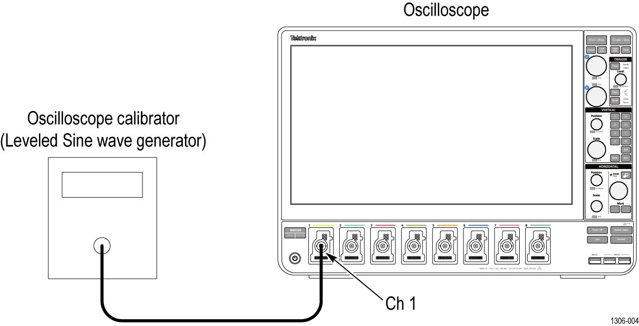
Check random noise, sample acquisition mode
This test checks random noise at 1 M Ω and 50 Ω for each channel, in Sample acquisition mode. You do not need to connect any test equipment to the oscilloscope for this test.
- Disconnect everything from the oscilloscope inputs.
- Tap File > Default Setup.
- Add the AC RMS measurement:
- Tap the Add New... Measure button.
- Set the Source to the channel being tested.
- In the Amplitude Measurements panel, double-tap the AC RMS measurement button to add the measurement badge to the Results bar.
- Tap outside the menu to close it.
- Double-tap the AC RMS measurement badge and tap Show Statistics in Badge to display statistics in the measurement badge.
- Tap the Filter / Limit Results panel.
- Turn on Limit Measurement Population.
- Set the limit to 100.
- Tap outside the menu to close it.
- Set up the Horizontal mode:
- Double-tap the Horizontal setting badge.
- Set Horizontal Mode to Manual.
- Set the Sample Rate to 6.25 GS/s.
- Set the Record Length to 2 Mpts.
- Tap outside the menu to close it.
- Double-tap the Channel badge of the channel being tested.
- Set the Vertical Scale value to 1 mV.
- Check 1 M Ω termination.
- In the Channel badge menu, tap 1 M Ω termination.
- Tap the Bandwidth Limit field and select the highest frequency listed.
- Set the channel Position value to 340 mdivs.
- Once the measurement count (N) in the AC RMS measurement badge reaches 100, record the AC RMS Mean value (the µ readout).
- Set the channel vertical Position value to 360 mdivs.
- Once the measurement count (N) in the measurement badge reaches 100, record the AC RMS Mean value (the µ readout).
- Average the two values and record the result in the 1 mV/div > Full row of the 1 MΩ column of the Test Result record.
- In the channel badge menu, tap the Bandwidth Limit field and select 250 MHz.
- Set the channel vertical Position value to 340 mdivs.
- Once the measurement count (N) in the measurement badge reaches 100, record the AC RMS Mean value (the µ readout).
- Set the channel vertical Position value to 360 mdivs.
- Once the measurement count (N) in the measurement badge reaches 100, record the AC RMS Mean value (the µ readout).
- Average the two values and record the result in the 1 mV/div > 250MHz limit row of the 1 MΩ column of the Test Result record.
- Tap the Bandwidth Limit field and select 20 MHz.
- Set the channel vertical Position value to 340 mdivs.
- Once the measurement count (N) in the measurement badge reaches 100, record the AC RMS Mean value (the µ readout).
- Set the channel vertical Position value to 360 mdivs.
- Once the measurement count (N) in the measurement badge reaches 100, record the AC RMS Mean value (the µ readout).
- Average the two values and record the result in the 1 mV/div > 20MHz limit row of the 1 MΩ column of the Test Result record.
- Check 50 Ω termination.
- In the Channel badge, set Termination to 50 Ω.
- Tap the Bandwidth Limit field and select the highest frequency listed.
- Set the channel vertical Position value to 340 mdivs.
- Once the measurement count (N) in the measurement badge reaches 100, record the AC RMS Mean value (the µ readout).
- Set the channel vertical Position value to 360 mdivs.
- Once the measurement count (N) in the measurement badge reaches 100, record the AC RMS Mean value (the µ readout).
- Average the two values and record the result in the 1 mV/div > Full row of the 50 Ω column of the Test Result record.
- Tap the Bandwidth Limit field and select 250 MHz.
- Set the channel vertical Position value to 340 mdivs.
- Once the measurement count (N) in the measurement badge reaches 100, record the AC RMS Mean value (the µ readout).
- Set the channel vertical Position value to 360 mdivs.
- Once the measurement count (N) in the measurement badge reaches 100, record the AC RMS Mean value (the µ readout).
- Average the two values and record the result in the 1 mV/div > 250MHz limit row of the 50 Ω column of the Test Result record.
- Tap the Bandwidth Limit field and select 20 MHz.
- Set the channel vertical Position value to 340 mdivs.
- Once the measurement count (N) in the measurement badge reaches 100, record the AC RMS Mean value (the µ readout).
- Set the channel vertical Position value to 360 mdivs.
- Once the measurement count (N) in the measurement badge reaches 100, record the AC RMS Mean value (the µ readout).
- Average the two values and record the result in the 1 mV/div > 20MHz limit row of the 50 Ω column of the Test Result record.
- Repeat 1 MΩ and 50 Ω tests at all V/div settings for the current channel.
- Repeat all tests for the remaining input channels.
- Double-tap the AC RMS measurement badge.
- Tap the Configure panel.
- Tap the Source 1 field and select the next channel to test.
- Double-tap the channel badge of the channel that you have finished testing and set Display to Off.
- Tap the channel button on the oscilloscope Settings bar of the next channel to test.
- Double-tap the channel badge for the channel being tested.
- Starting at step 6, repeat these procedures for each input channel.
Check random noise, High Res mode
This test checks random noise at 1 M Ω and 50 Ω for each channel in High Res acquisition mode. You do not need to connect any test equipment to the oscilloscope for this test.
- Disconnect everything from the oscilloscope inputs.
- Tap File > Default Setup.
- Double-tap the Acquisition badge and set Acquisition Mode to High Res.
- Add the
AC RMS measurement:
- Tap the Add New... Measure button to open the Add Measurements menu.
- Set the Source to the channel being tested.
- In the Amplitude Measurements panel, double-tap the AC RMS button to add the measurement badge to the Results bar.
- Tap outside the menu to close it.
- Double-tap the AC RMS measurement badge and tap Show Statistics in Badge to display statistics in the measurement badge.
- Tap the Filter/Limit Results panel.
- Turn on Limit Measurement Population.
- Set the limit to 100.
- Tap outside the menu to close it.
- Set up the Horizontal mode:
- Double-tap the Horizontal setting badge.
- Set Horizontal Mode to Manual.
- Set the Sample rate to 6.25 GS/s.
- Set the Record Length to 2 Mpts.
- Tap outside the menu to close it.
-
Check
1 M Ω termination as follows:
- Double-tap the Channel badge of the channel being tested.
- Set the Vertical Scale value to 1 mV.
- Set Termination to 1 M Ω.
- Tap the Bandwidth Limit field and select the highest frequency listed.
- Set the channel Position value to 340 mdivs.
- Once the measurement count (N) in the measurement badge reaches 100, record the AC RMS Mean value (the µ readout).
- Set the channel Position value to -340 mdivs.
- Once the measurement count (N) in the measurement badge reaches 100, record the AC RMS Mean value (the µ readout).
- Average the two values and record the result in the 1'mV/div > Full row of the 1 MΩ column of the random noise, High Res mode Test Result record.
- Tap the Bandwidth Limit field and select 250 MHz.
- Set the channel Position value to 340 mdivs.
- Once the measurement count (N) in the measurement badge reaches 100, record the AC RMS Mean value (the µ readout).
- Set the channel Position value to -340 mdivs.
- Once the measurement count (N) in the measurement badge reaches 100, record the AC RMS Mean value (the µ readout).
- Average the two values and record the result in the 1 mV/div > 250MHz limit row of the 1 MΩ column of the random noise, High Res mode Test Result record.
- Tap the Bandwidth Limit field and select 20 MHz.
- Set the channel Position value to 340 mdivs.
- Once the measurement count (N) in the measurement badge reaches 100, record the AC RMS Mean value (the µ readout).
- Set the channel Position value to -340 mdivs.
- Once the measurement count (N) in the measurement badge reaches 100, record the AC RMS Mean value (the µ readout).
- Average the two values and record the result in the 1 mV/div > 20MHz limit row of the 1 MΩ column of the random noise, High Res mode Test Result record.
-
Check
50 Ω termination as follows:
- In the Channel badge, set Termination to 50 Ω.
- Tap the Bandwidth Limit field and select the highest frequency listed.
- Set the channel Position value to 340 mdivs.
- Once the measurement count (N) in the measurement badge reaches 100, record the AC RMS Mean value (the µ readout).
- Set the channel Position value to -340 mdivs.
- Once the measurement count (N) in the measurement badge reaches 100, record the AC RMS Mean value (the µ readout).
- Average the two values and record the result in the 1 mV/div > Full row of the 50 Ω column of the random noise, High Res mode Test Result record.
- Tap the Bandwidth Limit field and select 250 MHz.
- Set the channel Position value to 340 mdivs.
- Once the measurement count (N) in the measurement badge reaches 100, record the AC RMS Mean value (the µ readout).
- Set the channel Position value to -340 mdivs.
- Once the measurement count (N) in the measurement badge reaches 100, record the AC RMS Mean value (the µ readout).
- Average the two values and record the result in the 1 mV/div > 250MHz limit row of the 50 Ω column of the random noise, High Res mode Test Result record.
- Tap the Bandwidth Limit field and select 20 MHz.
- Set the channel Position value to 340 mdivs.
- Once the measurement count (N) in the measurement badge reaches 100, record the AC RMS Mean value (the µ readout).
- Set the channel Position value to -340 mdivs.
- Once the measurement count (N) in the measurement badge reaches 100, record the AC RMS Mean value (the µ readout).
- Average the two values and record the result in the 1 mV/div > 20MHz limit row of the 50 Ω column of the random noise, High Res mode Test Result record.
- Repeat 1 MΩ and 50 Ω tests at all V/div settings for the current channel:
-
Repeat all tests for the remaining input channels:
- Double-tap the AC RMS measurement badge.
- Tap the Configure panel.
- Tap the Source 1 field and select the next channel to test.
- Double-tap the channel badge of the channel that you have finished testing and set Display to Off.
- Tap the channel button on the oscilloscope Settings bar of the next channel to test.
- Double-tap the channel badge for the channel being tested.
-
Starting at step 6, repeat these procedures for each input channel.
Check long term sample rate
This test checks the sample rate and delay time accuracy (time base).
- Connect the output of a time mark generator to the oscilloscope channel 1 input using a 50 Ω cable, as shown in the following illustration.
WARNING:Set the generator output to off or 0 volts before connecting, disconnecting, and/or moving the test hookup during the performance of this procedure. The generator is capable of providing dangerous voltages. - Set the time mark generator period to 80 ms. Use a time mark waveform with a fast rising edge.
- If it is adjustable, set the time mark amplitude to approximately 2 VP-P.
- Tap File > Default Setup.
- Tap the channel 1 button on the Settings bar.
- Double-tap the Channel 1 badge to open its Configuration menu.
- Set Termination to 50 Ω.
- Set Vertical Scale to 500 mV.
- Set the Position value to center the time mark signal on the screen.
- Tap outside the menu area to close it.
- Double-tap the Horizontal settings badge.
- Set the Horizontal Scale to 100 ns/div.
- Tap outside the menu area to close it.
- Double-tap the Trigger settings badge.
- Set Source to the channel being tested.
- Set the Level as necessary for a triggered display.
- Tap outside the menu area to close it.
- Double-tap the Horizontal settings badge.
- Adjust the Position value to move the trigger point to the center of the screen.
- Turn Delay to On and set Position to 80 ms.
- Set the Horizontal Scale to 100 ns/div.
- Observe where the rising edge of the marker crosses the center horizontal graticule line. The rising edge should cross within ±2 divisions of the vertical center graticule. Enter the deviation in the test record. Note:A 2.5 x 10⁻⁶ time base error is 2 divisions of displacement.
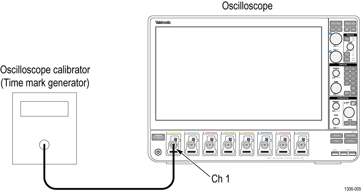
Check delta time measurement accuracy
This test checks the Delta-time measurement accuracy for a given instrument setting and input signal.
-
Connect a 50 Ω coaxial cable from the signal source to the oscilloscope channel 1, as shown in the following illustration.
WARNING:Set the generator output to Off or 0 volts before connecting, disconnecting, or moving the test hookup during the performance of this procedure. The generator is capable of providing dangerous voltages. - Tap File > Default Setup.
- Double-tap the badge of the channel under test to open its configuration menu.
-
Set the Vertical Scale to 5 mV/div.
- Set Termination to 50 Ω.
- Tap outside the menu to close it.
- Double-tap the Horizontal badge in the Settings bar.
- Set the Horizontal Scale to 10 ns/div.
- Set the Horizontal Mode to Manual.
- Set the Sample Rate to an unchecked value listed in the test record. Adjust the Record Length value until the correct Horizontal Scale value is set.
- Tap outside the menu to close it.
- Double-tap the Trigger settings badge.
- Set Source to the channel being tested.
- Set the Level as necessary for a triggered display.
- Tap outside the menu area to close it.
- Add a
Delay measurement for the channel under test:
- Tap the Add New... Measure button.
- Tap the Time Measurements panel.
- Double-tap the Delay measurement to add the measurement badge to the Results bar.
- Tap outside the menu to close it.
- Set the Delay measurement settings:
- Double-tap the Delay measurement badge.
- Check Show Statistics in Badge.
- Tap the Configure panel.
- Set both Source 1 and Source 2 to the channel under test.
- Set From Edge to the rising edge button.
- Set To Edge to the falling edge button.
- Tap the Reference Levels panel.
- Tap % in the Set Levels In control.
- Tap the Filter/Limit Results panel.
- Tap Limit Measurement Population to turn it on.
- Set the Limit field to 500.
- Tap outside the menu to close it.
-
Check the performance as follows:
- Set the calibrator signal source to the frequency and amplitude as shown in the test record.
Note:To provide consistent results, set the signal source frequency such that the zero crossing does not occur very close to the beginning or end of the record.
- Wait 5 - 10 seconds for the oscilloscope to acquire 500 samples before taking the reading.
- Enter the standard deviation readout in the Delay measurement badge in the test record. The value should be less than the upper limit shown in the test record.
- Repeat the check for each combination of oscilloscope and source signal settings in the test record.
- Set the calibrator signal source to the frequency and amplitude as shown in the test record.
-
Repeat tests for the remaining channels:
- Double-tap the channel badge of the channel that you have finished testing and set Display to Off.
- Tap the channel button of the next channel to test.
- Set the calibrator to 0 volts.
- Move the calibrator output to the next channel input to be tested.
- Repeat the procedure from step
3 until all channels have been tested. To change the source for the Delay measurement for each channel test:
- Double-tap the Delay measurement badge.
- Tap the Configure panel label.
- Set the Source 1 and Source 1 fields to the next channel to test.
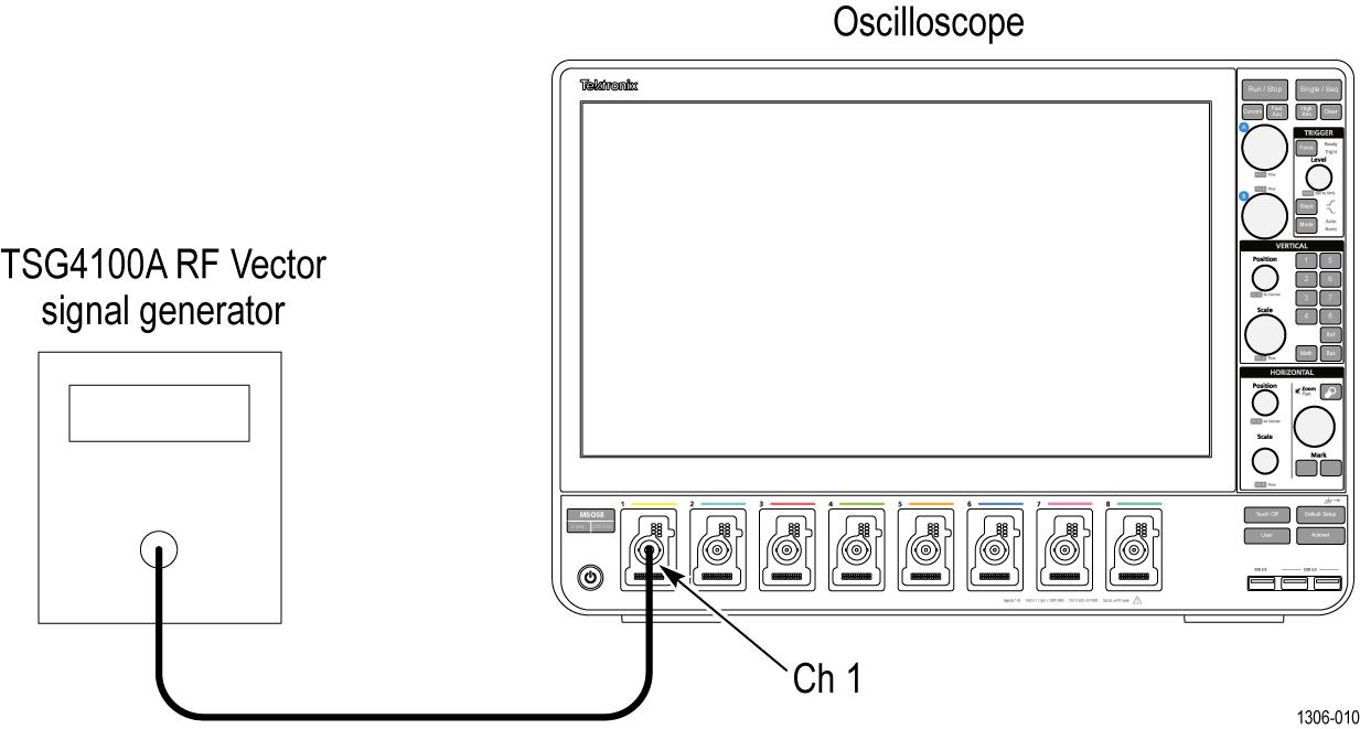
Check digital threshold accuracy
This test checks the threshold accuracy of the logic probe digital channels D0-D7 at 0 V and 25 °C, for all oscilloscope input channels.
| Note:Threshold Accuracy is a function of the logic probe only. It is a typical specification. The Threshold Accuracy test checks the typical logic probe performance, and may be considered a functional check of the oscilloscope digital input.
|
-
Connect the TLP058 digital probe to channel 1.
- Connect the DC voltage source to digital channel
D0.
WARNING:Set the generator output to Off or 0 volts before connecting, disconnecting, or moving the test hookup during the performance of this procedure. The generator is capable of providing dangerous voltages.
If you are using the Fluke 9500 calibrator as the DC voltage source, connect the calibrator head to the digital channel D0, using the BNC-to-0.1 inch pin adapter listed in the Required equipment table. Be sure to connect channel D0 to both the corresponding signal pin and to a ground pin on the adapter.
- Tap File > Default Setup. This resets the instrument and adds the channel 1 badge and signal to the display.
-
Display the digital channels and set the thresholds as follows:
- Double-tap the badge of the channel under test on the Settings bar.
- Double-tap the Threshold field at the bottom of the menu and set the value to 0 V.
- Tap Set All Thresholds. All thresholds are now set for the 0 V threshold check.
- Tap outside the menu to close it.
- Double-tap the Horizontal badge in the Settings bar.
- Set the Horizontal Scale to 10 ns/div.
- Tap outside the menu to close it.
- Set the calibrator DC voltage output (Vs) to -400 mV.
- Wait 1 second. Verify that the logic level is low on D0.
- Increment Vs by
+10 mV. Wait 1 second and check the logic level of the channel D0 signal display.
If the signal level is a logic low or is alternating between high and low, continue to increment Vs by +10 mV, wait 1 second, and check the logic level until the logic state is a steady high.
- Record this Vs value as Vs- for D0 of the test record.
- Double-tap the Trigger badge and set the Slope to Falling edge.
- Set the DC voltage source (Vs) to +400 mV.
- Wait 1 second. Verify that the logic level is high.
- Decrement Vs by
-10 mV. Wait 1 second and check the logic level of the channel D0 signal display.
If the signal level is a logic high or is alternating between high and low, continue to decrement Vs by -10 mV, wait 1 second, and check the logic level until the logic state is a steady low.
- Record this Vs value as Vs+ for D0 of the test record.
- Find the average using this formula: VsAvg = (Vs- + Vs+)/2.
- Record the average as the test result for D0 in the test record. The test result should be between the low and high limits.
- Repeat the procedure for all remaining digital channels as follows:
-
Repeat the procedure for all remaining input channels as follows:
- Move the TLP058 digital probe from channel 1 to channel 2.
- Set the generator output to 0 volts and Off.
- Repeat steps starting at 2 for the channel being tested (channel 2, channel 3, and so on).
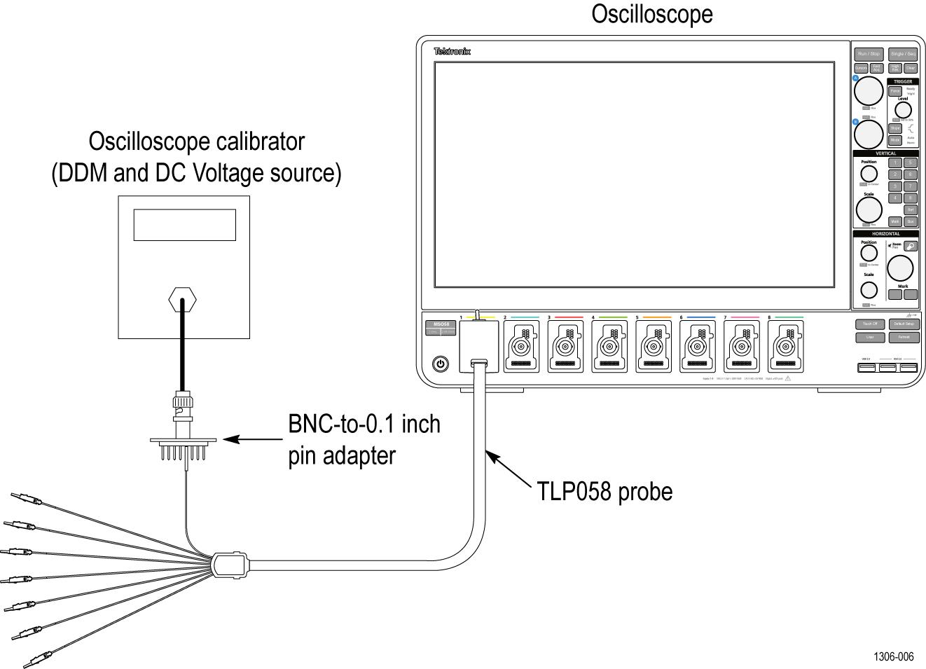
Check DVM voltage accuracy (DC)
This test checks the DC voltage accuracy of the Digital Volt Meter (DVM) option. The DVM option is available for free when you register the instrument at tek.com.
Procedure
- Connect the oscilloscope to a DC voltage source to run this test. If using the Fluke 9500 calibrator as the DC voltage source, connect the calibrator head to the oscilloscope channel to test.
WARNING:Set the generator output to Off or 0 volts before connecting, disconnecting, or moving the test hookup during the performance of this procedure. The generator is capable of providing dangerous voltages.
Check DVM voltage accuracy (AC)
This test checks the AC voltage accuracy of the Digital Volt Meter (DVM) option. The DVM option is available for free when you register the instrument at tek.com.
Procedure
- Connect the output of the leveled square wave generator (for example, Fluke 9500) to the oscilloscope channel 1 input.
WARNING:Set the generator output to Off or 0 volts before connecting, disconnecting, or moving the test hookup during the performance of this procedure. The generator is capable of providing dangerous voltages.
Check trigger frequency accuracy and maximum input frequency
This test checks trigger frequency counter accuracy. The trigger frequency counter is part of the free DVM and trigger frequency option that is available when you register the instrument at tek.com.
Procedure
Check AFG sine and ramp frequency accuracy
This test verifies the frequency accuracy of the arbitrary function generator. All output frequencies are derived from a single internally generated frequency. Only one frequency point of channel 1 is required to be checked.
- Connect a 50 Ω cable from the AFG Out connector to the frequency counter input as shown in the following figure.
Figure 1. Frequency/period test - Tap File > Default Setup to set the instrument to the factory default settings.
- Tap the AFG button to open the AFG menu.
- Set the arbitrary function generator output as follows:
Select menu Setting Output On Waveform Type Sine Frequency 1.000000 MHz Amplitude 1.00 VPP - Turn on the frequency counter:
- Double-tap the Trigger badge to open its menu.
- Set the Source field to the input channel being tested.
- Tap the Set to 50% button to obtain a stable display.
- Tap the Mode & Holdoff panel to open the Mode & Holdoff configuration menu
- In the Mode & Holdoff menu, set the Trigger Frequency Counter to On. The trigger frequency readout is at the bottom of the Trigger badge.
- Tap outside the menu to close it.
- Check that the reading of the frequency counter is between 0.999950 MHz and 1.000050 MHz. Enter the value in the Test record.
- Set the arbitrary function generator output as follows:
Select menu Setting Waveform Type Ramp Frequency 500 kHz - Check that reading of the frequency counter is between 499.975 kHz and 500.025 kHz. Enter the value in the Test record.
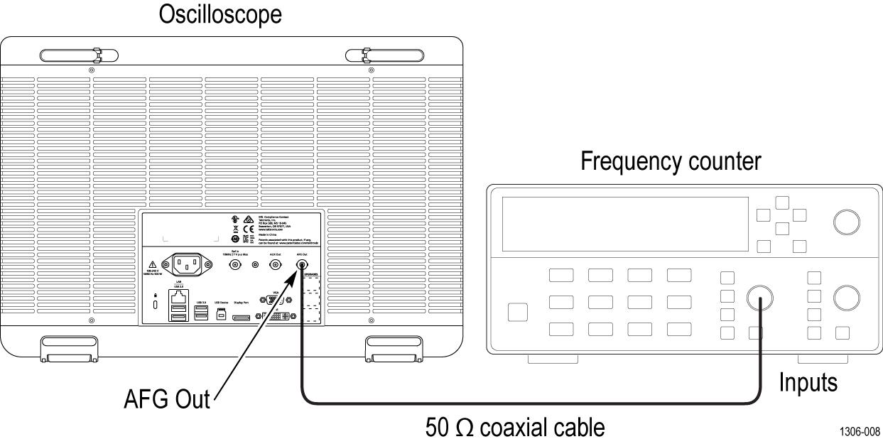
Check AFG square and pulse frequency accuracy
This test verifies the frequency accuracy of the arbitrary function generator. All output frequencies are derived from a single internally generated frequency. Only one frequency point of channel 1 is required to be checked.
- Connect the arbitrary function generator to the frequency counter as shown in the following figure.
Figure 1. Frequency/period test - Tap File > Default Setup to set the instrument to the factory default settings.
- Tap the AFG button to open the AFG menu.
- Set the arbitrary function generator as follows:
Select menu Setting Waveform Type Square Frequency 1.000000 MHz Amplitude 1.00 VPP Output On - Turn on the frequency counter:
- Double-tap the Trigger badge to open its menu.
- Set the Source field to the input channel being tested.
- Tap the Set to 50% button to obtain a stable display.
- Tap the Mode & Holdoff panel to open the Mode & Holdoff configuration menu
- In the Mode & Holdoff menu, set the Trigger Frequency Counter to On. The trigger frequency readout is at the bottom of the Trigger badge.
- Tap outside the menu to close it.
- Check that the frequency counter readout is between 0.999950 MHz and 1.00005 MHz. Enter the value in the Test record.
- Set up the arbitrary function generator as follows:
Select menu Setting Waveform Type Pulse - Check that reading of the frequency counter is between 0.999950 MHz and 1.000050 MHz. Enter the value in the Test record.
Check AFG signal amplitude accuracy
This test verifies the amplitude accuracy of the arbitrary function generator. All output amplitudes are derived from a combination of attenuators and 3 dB variable gain. Some amplitude points are checked. This test uses a 50 Ω terminator. It is necessary to know the accuracy of the 50 Ω terminator in advance of this amplitude test. This accuracy is used as a calibration factor.
- Connect the 50 Ω terminator to the DMM as shown in the following figure and measure the resistance value.
Figure 1. 50 Ω terminator accuracy - Calculate the 50 Ω calibration factor (CF) from the reading value and record as follows:
Table 1. CF (Calibration Factor) = 1.414 × ((50 / Measurement Ω) + 1) Measurement (reading of the DMM) Calculated CF Examples:- For a measurement of 50.50 Ω, CF = 1.414 ( 50 / 50.50 + 1) = 2.814.
- For a measurement of 49.62 Ω, CF = 1.414 ( 50 / 49.62 + 1) = 2.839.
- Connect the arbitrary function generator output to the DMM as shown in the following figure. Be sure to connect the 50 Ω terminator to the AFG Out connector.
Figure 2. Amplitude test - Tap the AFG button and set up the arbitrary function generator output as follows:
Select menu Setting Waveform Type Sine Frequency 1.000000 kHz Amplitude 30 mVPP Load Impedance 50 Ω Output On - Measure the AC RMS voltage readout on the DMM.
- Multiply the DMM voltage by the calculated CF to get the corrected peak to peak voltage. Enter the resulting value in the Measurement field in the following table.
- Change the AFG output amplitude to the next value in the table.
- Repeat steps 5 through 7 for each amplitude value. Check that the peak to peak voltages are within the limits in the table below. Enter the values in the test record.
Waveform Type Frequency Amplitude Measurement Range Sine 1.000 kHz 30.0 mVPP 28.55 mVPP - 31.45 mVPP Sine 1.000 kHz 300.0 mVPP 294.5 mVPP - 305.5 mVPP Sine 1.000 kHz 800.0 mVPP 787.0 mVPP - 813.0 mVPP Sine 1.000 kHz 1.500 VPP 1.4765 VPP - 1.5235 VPP Sine 1.000 kHz 2.000 VPP 1.969 VPP - 2.031 VPP Sine 1.000 kHz 2.500 VPP 2.4615 VPP - 2.5385 VPP
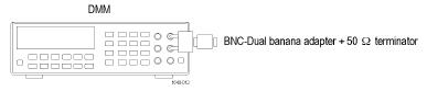
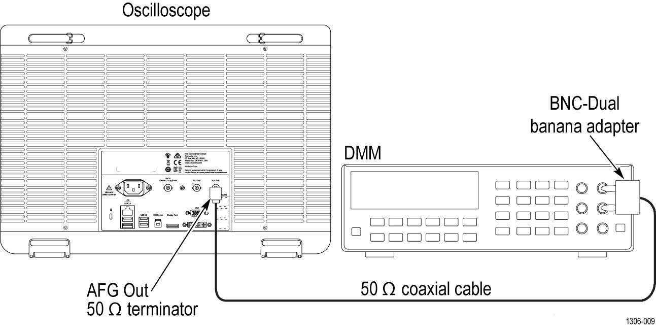
Check AFG DC offset accuracy
This test verifies the DC offset accuracy of the arbitrary function generator. This test uses a 50 Ω terminator. It is necessary to know the accuracy of the 50 Ω terminator in advance of this test. This accuracy is used as a calibration factor.
- Connect the 50 Ω terminator to the DMM as shown in the following figure and measure the resistance value.
Figure 1. 50 Ω terminator accuracy - Calculate the 50 Ω calibration factor (CF) from the reading value and record as follows:
Table 1. CF (Calibration Factor) = 0.5 × (( 50 / Measurement Ω) + 1) Measurement (reading of the DMM) Calculated CF
Examples:- For a measurement of 50.50 Ω, CF = 0.5 ( 50 / 50.50 + 1) = 0.9951.
- For a measurement of 49.62 Ω, CF = 0.5 ( 50 / 49.62 + 1) = 1.0038.
- Connect the arbitrary function generator output to the DMM as shown in the following figure. Be sure to connect the 50 Ω terminator to the arbitrary function generator AFG Output connector.
Figure 2. DC offset tests - Tap the AFG button and set up the arbitrary function generator as follows:
Select menu Setting Waveform Type DC Offset + 1.25 V Output On - Measure the voltage readout on the DMM.
- Multiply the DMM voltage by the calculated CF to get the corrected offset voltage. Enter the resulting value in the Measurement field in the following table.
Function Offset Measurement Range DC + 1.25 Vdc Vdc 1.23025 Vdc to 1.26975 Vdc DC 0.000 Vdc Vdc - 0.001 Vdc to + 0.001 Vdc DC - 1.25 Vdc Vdc -1.26975 Vdc to -1.23025 Vdc - Change the AFG output amplitude to the next value in the table, measure the voltage readout on the DMM, multiply the DMM readout by the calculated CF to get the corrected offset voltage, and enter the resulting value in the Measurement field in the table.
- Verify that the corrected offset measurements are within the range.
Help us improve our technical documentation. Provide feedback on our TekTalk documentation forum.