Soaring demand for cell phones, pagers mobile radios and base-stations, is putting pressure on test engineers to shorten production test time. This may require selection of new test equipment that can improve throughput and accuracy in several areas, including a wide variety of DC and low-frequency board-level tests, and battery testing or simulation.
Battery Characteristics
To test portable communication devices under realistic conditions, you may need a power supply that can simulate a battery under various discharge states. This requires a power supply with a variable output impedance, which closely duplicates the voltage characteristics of a battery during energy drain. These power supplies should also have an ultra-wide bandwidth output stage to minimize transient voltage droop and recovery time to allow end-of-life rechargeable battery testing. In addition to accurate battery simulation, it is very helpful to have a read-back power supply that can accurately measure load currents. This eliminates the need for a separate instrument and calculation of dynamic power consumption for comparison to test specs.
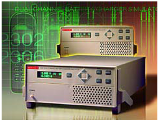
The Keithley Instruments Models 2302 and 2306 are typical of this new breed of power supply specifically designed for portable telecommunication product testing. The 2306 even has a second channel that allows seamless transfer of power from the units battery channel to its charger channel while keeping the device under test (DUT) powered. This allows accurate simulation of a DUTs battery/power supply circuit as it switches to the charger when battery voltage is low, thereby allowing realistic testing of the DUT under these conditions.
Switching Systems for Board Testing
The principal board-level tests on wireless devices are internal voltages, current drains and power consumption. To speed up multiple measurements, a typical test configuration includes automated signal routing equipment that ties different instruments to several points on the DUT. However, the test system designer must balance throughput and accuracy by selecting the appropriate switching system.
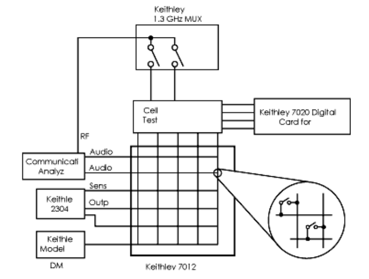
Simplified diagram of a cell phone test system using a matrix switch configuration. (A multiplexer topology also could be used; see text.)When you consider the number of signal connections made through the switching system (Figure 1), it becomes apparent that switching consumes a major portion of test cycle time. Several design factors affect switching time.
Switch Configurations
The current trend in switching system designs is to use one or two basic topologies.The most common ones are the 1 x m multiplexer and the n x m matrix, where the number of inputs, n, is switched to any one of the m outputs. Multiplexer designs are easiest to construct and usually are the most cost effective. However, overall throughput may benefit from a matrix design, since any row can be connected to any column at any time. Figure 2 shows two common types of multiplexers. The standard multiplexer consists of a simple design that uses 1 x m relays (Figure 2a,) or a combination of smaller relays, and works well at low frequencies.
For large values of m and high frequencies, the unterminated stubs may introduce signal degradation due to reflection effects. An improved design utilizing tree switching (Figure 2b) eliminates stubs but introduces additional relays and insertion loss into the signal path and increases system cost.
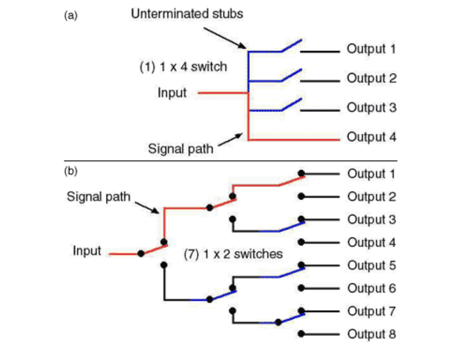
Multiplex configurations: (a) 1 x 4 multiplex using a single 1 x 4 switch (b) 1 x 8 multiplex using seven 1 x 2 switches in a tree configuration. Multiplexing can be done with relays or solid-state switching devices. Solid state switches tend to have settling times of a few hundred microseconds; reed relay settling times typically range from three to 10 milliseconds, but cost less. Switching devices are normally installed on a switch card housed in the card cage of a mainframe that also includes drive lines and test instruction parameters.
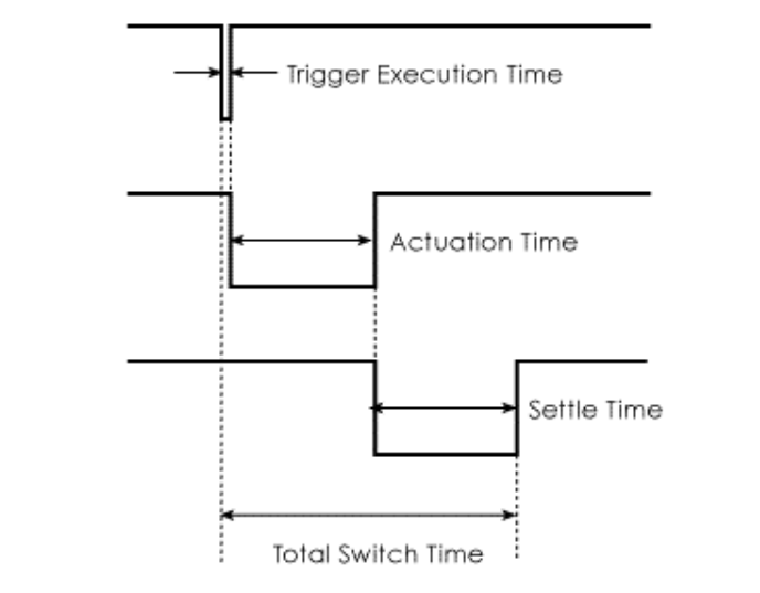
The system may connect these devices through several ports, such as external trigger lines, input/output signals, and remote control connections (GPIB, RS-232, etc.). See Figure 1.Switching Times Switching time is another important specification. It is the time it takes to disconnect one signal and connect another one to the measurement instrument. Total switching time is a combination of trigger execution time, actuation time and settle time. (Figure 3.)
The majority of a multiplexers switching time is the combination of the time it takes for contacts to move across the switch gap (actuation time) and the time it takes for contact bounce to stop (settle time.)Along with switching time, a major consideration is the bandwidth of the signal path. A lot of new switch cards have recently come to market with broadband capabilities. However, keep in mind the rule that bandwidth costs money, which applies to RF switching systems as well as other signal propagation systems. Specify only what you need.
Measuring Instruments
Typically, production testing is computer controlled with individual instruments and the switching system connected to a PC on the IEEE-488 bus. The test setup may also involve the use of a device handler with a fixture that holds the DUTs. A device handler can consume up to 100 ms during unloading and loading of a DUT. As discussed earlier, the switching system can consume several milliseconds for each actuation. Modern GPIB instruments can perform measurements at rates as high as 2000 readings per second, or about 0.5 ms/reading. The IEEE-488 bus can transfer data at about 1 Mb/s, so it is least likely to limit test system throughput.
There will be circumstances when factors other than speed affect instrument selection criteria. Most often, accuracy will be a major consideration. Look for programmable instrument features that allow accuracy and measurement speed tradeoffs, such as the following:
Integration Rate
This is the time it takes the instruments A/D converter to look at the input signal. The integration time affects the usable measurement resolution, the amount of reading noise, and the ultimate reading rate of the measurement. The optimum integration time setting involves a tradeoff between speed and common mode or normal mode noise.
If speed is the most important consideration, then a small integration rate is used, such as 0.01 power line cycles (PLCs), at the expense of reading additional noise and getting less usable resolution. The greatest noise reduction is achieved by using integer PLC values.
Ranging
Instrument measurement rates are usually stated for a fixed measurement range. While some instruments have fast autoranging features, actual speed is not predictable. If the feature is programmable, autoranging should not be used when optimum speed is required; a fixed range is the only way to ensure timing precision.
Filters
When digital filters are available, measurement rates are typically stated with all filters turned off. Although filtering improves noisy measurements, it also slows the rate of measurement. With a digital filter, an instrument takes a number of A/D conversions and averages them before displaying the result. The greater the number of conversions averaged, the slower the measurement rate.
Autozero
During autozero the A/D conversion is switched through four distinct periods: signal integrate, reference integrate, zero integrate and calculate. With autozero disabled, the A/D conversion does not use the zero integrate or reference integrate periods and measurement speed is increased. However, it also means the readings could drift slightly after a period of time. Assuming that a small amount of drift can be tolerated over several measurements, then you can program the instrument to autozero only at the start of a test cycle,
Trigger Delay
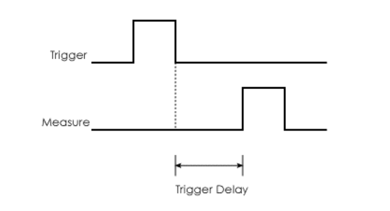
This is the period between the leading edge of the trigger signal and the time when the instrument starts the A/D conversion. This delay is used when signals have significant settling times, for example, in a multi-channel test system with relays used to make connections to various inputs. Starting the A/D conversion before the signal is settled could result in a noisy, inaccurate measurement. By reading the relay or switching system spec sheet, you can determine maximum settling time and program the trigger delay so it is only as long as necessary.
Display
Updating an instruments front panel display takes time. In applications where speed is critical, the display should be disabled, particularly in applications where you only need a digital pass/fail signal at the end of each test.
Besides programmability, there are advantages to storing as much of the test sequence as possible in instrument memory. Some instruments are designed to store up to 100 or more test configurations. By calling up the test sequence from instrument memory, external bus traffic between the host PC and the instrument is kept to a minimum. This shortens the data transmission part of the test cycle. Using an instrument with a comparator circuit and sending only a pass/fail signal as mentioned above, instead of actual measurement values, reduces transmission time and total test time even more.
