THIS APPLICATION NOTE
- Explains the basic setup of a mixed signal oscilloscope (MSO)
- Tells how to interpret the logic signal display on a Tektronix MSO
- Explains how to easily identify and measure setup and hold violations in digital designs using an MSO
Introduction
Timing relationships between signals are critical to reliable operation of digital designs. With synchronous designs, the timing of the clock signal relative to data signals is especially important.
Using a mixed signal oscilloscope, the timing relationships between multiple logic inputs and a clock signal can easily be determined. Setup & Hold triggering automates this clock-to-data timing determination
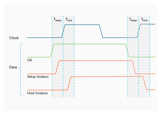
Setup Time is the time the input data signals are stable (either high or low) before the active clock edge occurs. Hold Time is the time the input data signals are stable (either high or low) after the active clock edge occurs. Setup and Hold Times are specified in component data sheets for synchronous devices (such as flip-flops) and must be met to assure that the component will behave correctly and reliably.
Based on their ability to capture both analog and digital representations of signals and display them in a time-correlated format, mixed signal oscilloscopes (MSOs) are ideal for verifying the signal integrity of the digital signals and debugging digital circuits. This application note uses a 5 Series MSO for illustration. The 2, 4, 5 and 6 Series MSOs operate identically. MSO2000 and MSO5000 Series oscilloscopes follow the same principles, but the user interface differs. They all combine the performance of a professional grade oscilloscope with the basic functions of a logic analyzer. The 3 Series MDO, MDO3000 and MDO4000 Series mixed domain oscilloscopes also offer 16-channel logic analyzer capabilities. Throughout this application note, any features or capabilities referred to in MSOs are also available in MDO products. For information on the features in each series, please visit tek.com.
MSO Setup
UNDERSTANDING DIGITAL TIMING RESOLUTION (DIGITAL SAMPLE RATE)
An important MSO acquisition specification is the timing resolution used for capturing digital signals. The sample rate varies between MSO models. It is important to understand your timing measurement resolution, especially when making judgments on setup and hold times. Table 1. Setup and hold specifications for ICs are often a few nanoseconds or less. When testing them with the digial logic inputs of your MSO, it is important to consider the timing resolution of the logic input.
DIGITAL SAMPLE RATES AND RECORD LENGTH TABLE FOR SETUP AND HOLD APP NOTE
| DIGITAL TIMING RESOLUTION | RECORD LENGTH | ||
| 2 Series MSO | 2 ns | 10 Mpoints | |
| 3 Series MDO | Main acquisition | 2 ns | 10 Mpoints |
| MagniVu acquisition | 121.2 ps | 10,000 points | |
| 4 Series B MSO | 160 ps | 31.25 Mpoints; 62.5 Mpoints optional | |
| 5 Series B MSO | 160 ps | 62.5 Mpoints; 125 Mpoints optional | |
| 6 Series B MSO | 20 ps on 2 channels 40 ps on 4 channels 80 ps on >4 channels |
62.5 Mpoints; up to 1 Gpoints optional | |
| MSO5000 Series | Main acquisition | 2 ns | 25 Mpoints; up to 250 Mpoints optional |
| MagniVu acquisition | 60.6 ps | 10,000 points | |
| MDO4000 Series | Main acquisition | 2 ns | 20 Mpoints |
| MagniVu acquisition | 60.6 ps | 10,000 points | |
| MDO3000 Series | Main acquisition | 2 ns | 10 Mpoints |
| MagniVu acquisition | 121.2 ps | 10,000 points | |
| MSO2000 Series | 1 ns (2 ns when two probes are used) | 1 Mpoints |
Table 1.Setup and hold specifications for ICs are often a few nanoseconds or less. When testing them with the digial logic inputs of your MSO, it is important to consider the timing resolution of the logic input.
SETTING DIGITAL THRESHOLDS
A mixed signal oscilloscope’s digital channels view a digital signal as either a logic high or logic low, just like a digital circuit views the signal. This means as long as ringing, overshoot and ground bounce do not cause logic transitions, these analog characteristics are not of concern to the MSO. Just like a logic analyzer, an MSO uses a user-specified threshold voltage to determine if the signal is logic high or logic low.
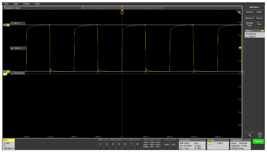
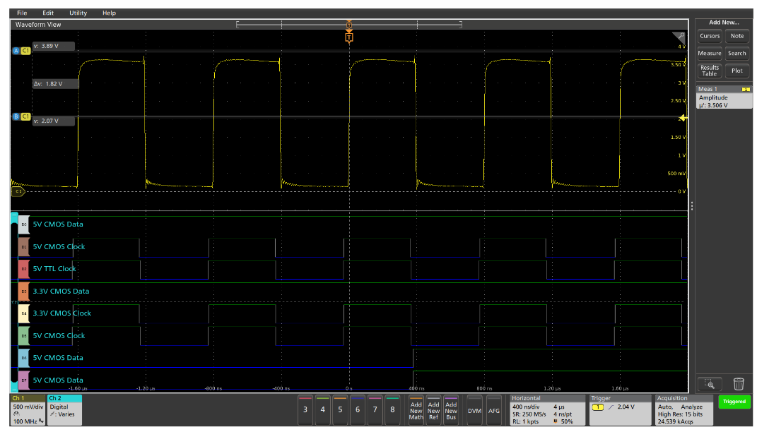
The MSO’s analog channel can be used to quickly check the logic swing of your digital signal. In Figure 1, the oscilloscope automatically measures the digital signal amplitude as about 3.6 V. For logic families with symmetrical voltage swings like CMOS, the threshold is at half of the signal amplitude. However, for logic families with asymmetrical voltage swings like TTL (Transistor-Transistor Logic), you typically need to consult the component data sheet and define the threshold as half-way (TTL Vthreshold = 1.4V) between the logic device’s maximum low-level input voltage (TTL VIL = 0.8V) and minimum high-level input voltage (TTL VIH = 2.0V) values.
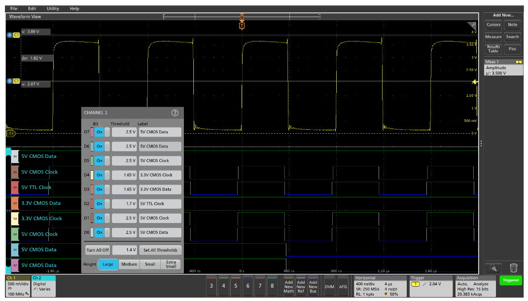
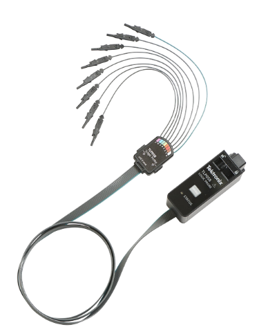
Most Tektronix MSOs provide per-channel threshold settings that are useful in debugging circuits with mixed logic families. Figure 2 shows the 5 Series MSO measuring multiple logic signals with an 8-channel TLP058 probe. The TTL signal threshold is set to 1.7 V, the 3.3 V CMOS signal thresholds are set to 1.65V, and the 5 V CMOS signal thresholds are set to 2.5 V, enabling reliable acquisition of the various logic signals at the same time.
For the 3 Series MDO, MSO2000 and MDO3000 Series, the thresholds are adjusted per probe pod (a grouping of 8 channels) and therefore, the TTL signals would be on one pod while the LVPECL signals would be on the second pod.
INTERPRETING THE COLOR-CODED DIGITAL WAVEFORM DISPLAY
Digital timing waveforms look very similar to analog waveforms except only logic highs and lows are shown. To make analysis easier, Tektronix MDO/MSO oscilloscopes show logic lows as blue and logic highs as green on the digital waveforms, allowing you to see the logic value even if a transition is not visible. The waveform label color also matches the probe color-coding to make it easier to see which signal corresponds to which test point, as shown in Figure 3.
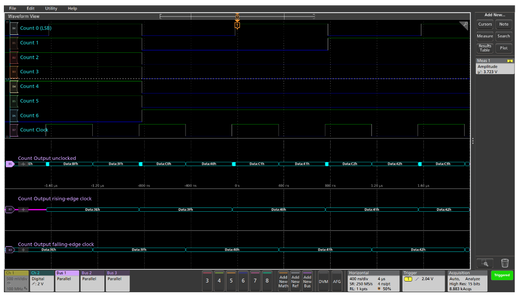
The digital timing waveforms can be grouped to create a bus. One digital signal is defined as the least significant bit and the other digital signals represent the other bits of the binary value up to the most significant bit. The oscilloscope will then decode the bus into a binary or hex value.
REMOVING TIMING SKEW BETWEEN CHANNELS
Every Tektronix MDO or MSO series oscilloscope has a compatible logic probe. To simplify digital measurements, the oscilloscope compensates for the propagation delay of the logic probe. Therefore, there are no digital channel probe deskew adjustments.
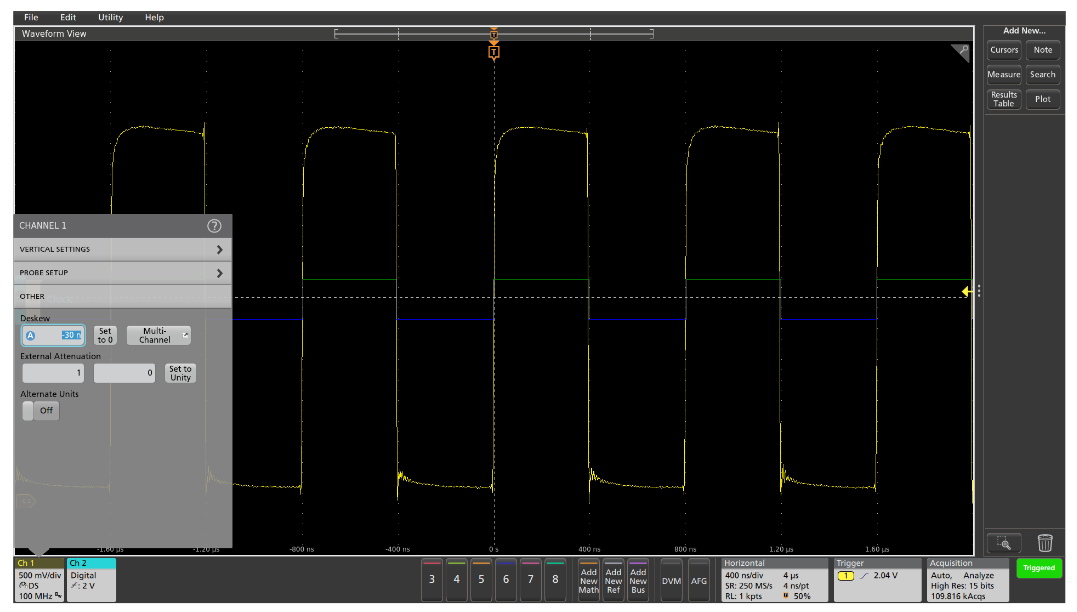
However, for better time-correlation measurements between the analog and digital waveforms, it’s important to remove the analog to digital time skew. In the example shown in Figure 5, to align the analog channels with the digital channels, the 2 V (50% amplitude) position on the analog waveform is time-aligned with the digital signal transitions which occur at the 2 V threshold. The deskew value is manually adjusted to align the analog channel to the digital channel. This deskew process needs to be repeated for any other analog channels.
Analog channel skews should be checked when the analog probes are changed and the digital thresholds should be checked when measuring a different logic family. With the threshold and skews configured, the oscilloscope is ready for verifying and debugging digital circuits.
FLIP-FLOP TIMING MEASUREMENTS
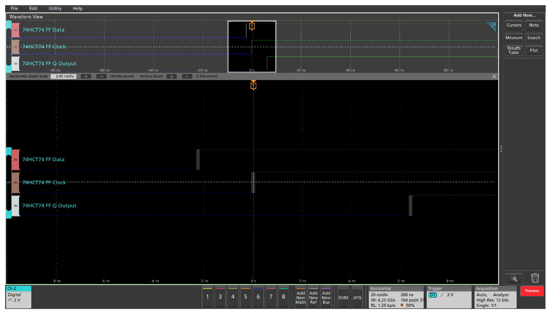
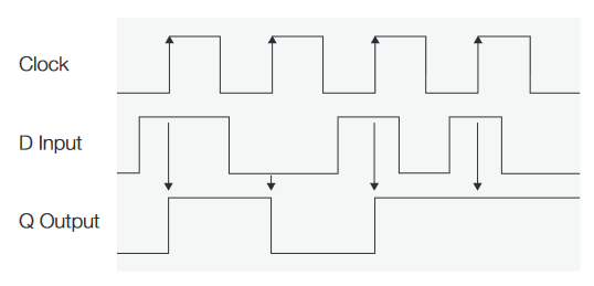
The simplest synchronous logic device is a flip-flop. The logic state of the D Input appears at the Q Output only after the rising clock edge (after the D-Flip-Flop propagation delay). An MSO is an ideal tool to verify the operation of a flip-flop and debug digital circuits.
At first glance, as shown in Figure 7, the flip-flop looks like it is working as expected. The data signal has been stable for several nanoseconds before the rising edge of the clock, and the data remains stable for many nanoseconds after the clock edge. The propagation from clock edge to the Q output is about 6 ns.
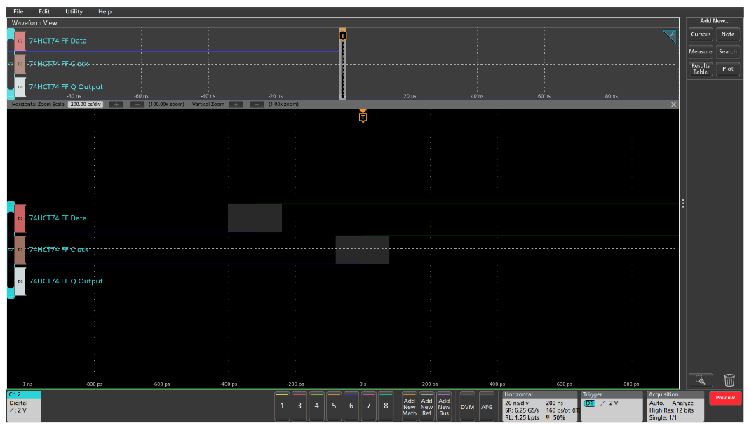
But Figure 8 shows an instance where the data signal is transitioning just 300 ps before the clock edge, well below the 15 ns setup time specification – a setup time violation. Notice that the Q output does not change state as expected.
Notice the gray regions around the signal transitions in Figure 8. The MSO displays these regions to indicate the timing uncertainty related to the digital sample rate.
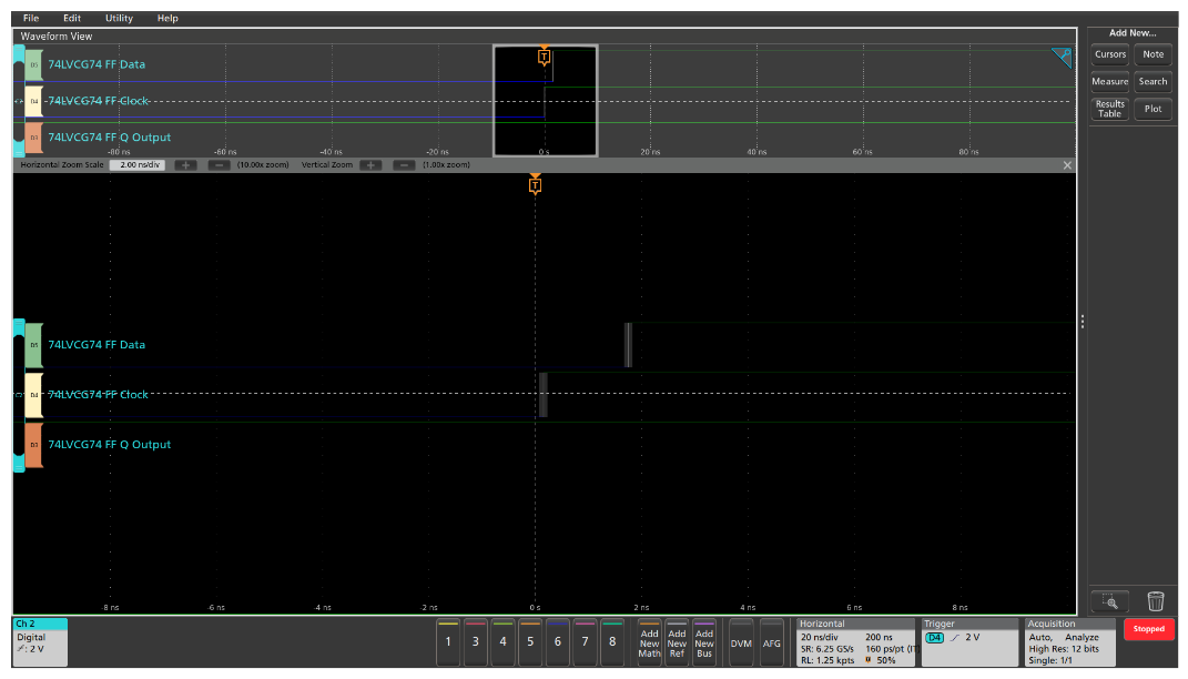
Figure 9 shows an instance where the data signal is transitioning about 300 ps after the clock edge. This is well below the 3 ns hold time specification – a hold time violation. Again, notice that the Q output does not change state as expected.

Capturing Setup and Hold Violations
MSOs have a specialized trigger mode designed to automatically capture every setup and/or hold violation. The setup and hold trigger measures the timing relationship between the clock and data signal (or, with some MSOs, data signals) and captures signals when the setup time or hold time is below the specification. This capability simplifies debug, but also can be used for unattended monitoring of a design.
After consulting the 74LVCG74 component data sheet, the setup and hold trigger parameters (2 ns and 1 ns, respectively) are set to capture any violations, as shown in Figure 10. The MSO automatically triggers on the first input condition that violates the specified parameters.
In the previous example, setup and hold triggers were used on the inputs to the flip-flop. Another approach is to trigger on signal errors on the output of the device, and capture the input signals for analysis.
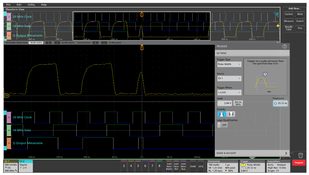
In the next example, an older design based on the 74LS74 low-power Schottky TTL technology, is exhibiting intermittent errors. The minimum output voltage for a high is 2.4 V, so all high output signals should be at least that high. The design is based on a 20 MHz clock (50 ns period), so all output pulses should be at least that wide.
Armed with these facts, the oscilloscope can quickly determine if the output signal is behaving as expected, and capture the inputs and outputs if it is not. Figure 11 shows a pulse width trigger finding a glitch, a signal where the pulse width is less than half of the minimum expected pulse width for this design.

Not only are there intermittent glitches on the output of the flip-flop, but some appear to have a low amplitude. Figure 12 shows a runt trigger capturing narrow, low-amplitude pulses which do not meet the component’s specification.

Using either of these trigger setups, you can capture the input and output signals. Figure 13 shows a setup time measurement with cursors that clearly indicates a setup time violation (about 6 ns, which is much lower than the 20 ns minimum value).
Mixed signal oscilloscopes combine basic logic analyzer functionality with the analog signal analysis of an oscilloscope. Tektronix MSOs and MDOs include setup and hold triggering, pulse triggering, and high resolution digital sampling to facilitate fast digital debugging.
Find more valuable resources at TEK.COM
Copyright © Tektronix. All rights reserved. Tektronix products are covered by U.S. and foreign patents, issued and pending. Information in this publication supersedes that in all previously published material. Specification and price change privileges reserved. TEKTRONIX and TEK are registered trademarks of Tektronix, Inc. All other trade names referenced are the service marks, trademarks or registered trademarks of their respective companies.
01/24 55W-61095-1


