Introduction
Semiconductor materials used in power electronics are transitioning from silicon to wide bandgap semiconductors such as silicon carbide (SiC) and gallium nitride (GaN) due to their superior performance in automotive and industrial applications. GaN and SiC enable smaller, faster and more efficient designs. Regulatory and economic pressures continue to push efficiency gains in high-voltage power electronics designs. The power-density advantages of smaller and lighter designs are particularly evident in space-constrained and/or mobile usages such as electric vehicles, but compact power electronics are more broadly desirable as well, especially from the standpoint of reduced system cost. At the same time, efficiency is growing in importance as governments introduce financial incentives and more stringent energy-efficiency regulations.
Guidelines issued by global entities, such as the European Union’s Eco-design Directive, the United States Department of Energy 2016 Efficiency Standards, and China’s Quality Certification Centre (CQC) Mark govern energy efficiency requirements for electrical products and equipment. The need to enact greater energy efficiency in power electronics stretches from the point of power generation to the point of consumption, as illustrated in Figure 1. Power converters operate at multiple stages throughout the generation, transmission, and consumption chain, and, because none of those operations is 100% efficient, some power loss occurs at each step. Chiefly due to energy lost as heat, these reductions in overall efficiency multiply throughout the cycle. [1]

When designing power converters, a 0% power loss is ideal as illustrated in Figure 2.

However, switching losses are inevitable. So, the goal is to minimize the losses through design optimization.Design parameters that are related to efficiency must be rigorously measured.
A typical converter would have an efficiency of about 87% to 90%, meaning that 10% to 13% of the input power is dissipated within the converter, mostly as waste heat. A significant portion of this loss is dissipated in the switching devices such as MOSFETs or IGBTs. [2]

Ideally, the switching device is either “on” or “off” as shown in Figure 3 and instantaneously switches between these states. In the “on” state, the impedance of the switch is zero ohms and no power is dissipated in the switch, regardless of how much current is flowing through it. In the “off” state, the impedance of the switch is infinite, and zero current is flowing, so no power is dissipated.
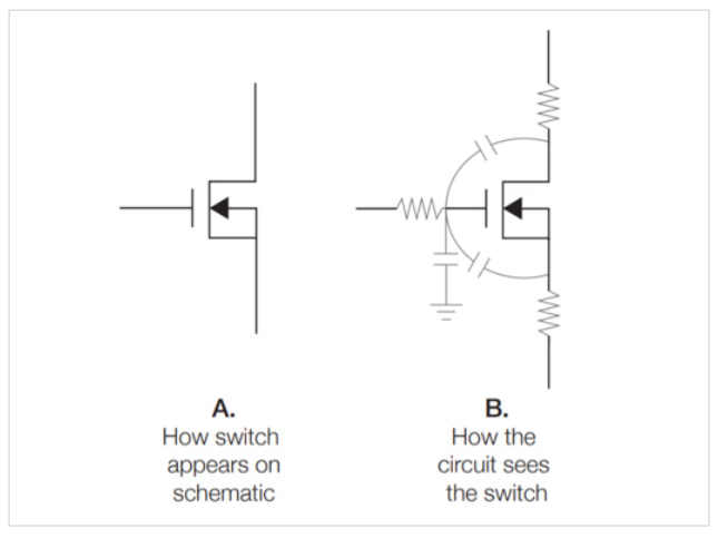
In practice, power is dissipated during the transition between “on” and “off” (turn-off) and between “off” and “on” (turn-on). These non-ideal behaviors occur because of parasitic elements in the circuit. As shown in Figure 4, the parasitic capacitances on the gate slow down the switching speed of the device, extending the turn-on and turn-off times. The parasitic resistances between the MOSFET drain and source dissipate power whenever drain current is flowing. [2]
There’s also reverse recovery loss of the body diode in the MOSFET to consider. Reverse recovery time of the diode is a measure of the switching speed in the diode and thus affects the switching losses in the converter design.
Therefore, design engineers will need to measure all these timing parameters in order to keep the switching losses at minimum and thus design more efficient converters.
The preferred test method to measure the switching parameters of MOSFETs or IGBTs is the “Double Pulse Test” method. This application note will describe the Double Pulse Test and how it’s implemented. In particular, this application note will explain how to generate pulses with the Tektronix AFG31000 Arbitrary Function Generator and measure important parameters with a 4, 5 or 6 Series MSO oscilloscope.
What is the Double Pulse Test?
Double Pulse Test is a method to measure the switching parameters and evaluate the dynamic behaviors of power devices. Users of this application typically want to measure the following switching parameters: [3]
- Turn-on Parameters: Turn-on delay (td(on)), rise time (tr), ton (turn-on time), Eon (On Energy), dv/dt and di/dt. Energy loss is then determined. [4]
- Turn-off Parameters: Turn-off delay (td(off)), fall time (tf),toff (turn-off time), Eoff (Off Energy), dv/dt and di/dt. Energy loss is then determined. [4]
- Reverse Recovery Parameters: trr (reverse recovery time), Irr (reverse recovery current), Qrr (reverse recovery charge), Err (reverse recovery energy), di/dt and Vsd (forward on voltage). [4]
This test is performed to:
- Guarantee specifications of power devices like MOSFETs and IGBTs.
- Confirm actual value or deviation of the power devices or power modules.
- Measure these switching parameters under various load conditions and validate performance across many devices.
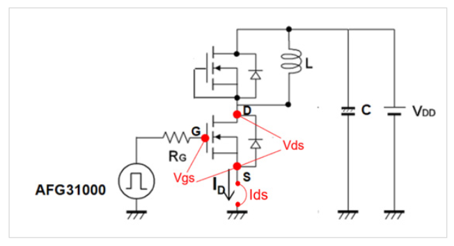
A typical Double Pulse Test circuit is shown in Figure 5.

The test is done with an inductive load and a power supply.The inductor is used to replicate circuit conditions in a converter design. The power supply is used to provide voltage to the inductor. The AFG31000 is used to output pulses that trigger the gate of the MOSFET and thus turns it on to start conduction of current.
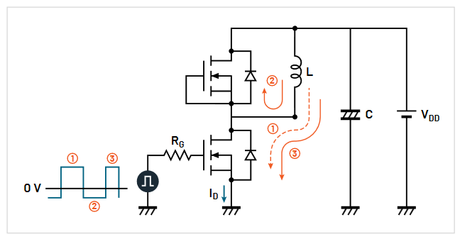
Figure 6 shows the current flow within the different stages of the test for a Double Pulse Test with MOSFETs. The same current flow would apply when using IGBTs as shown in Figure 7.
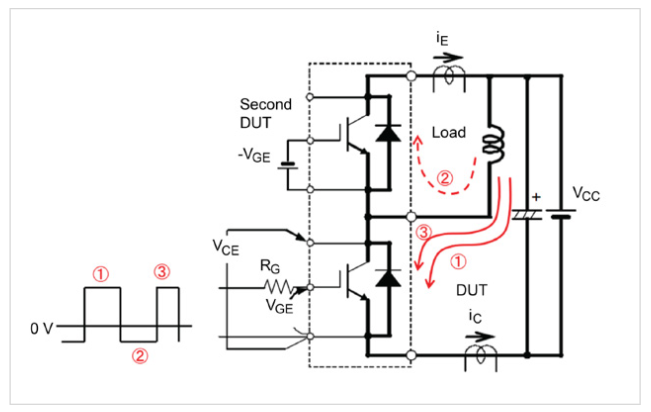

Figure 8 shows typical measurements taken on the low side MOSFET or IGBT. Here are the different stages of the Double Pulse Test (These stages refer to Figures 6, 7 and 8)
- The first step, represented by turn-on pulse number 1, is the initial adjusted pulse width. This establishes current in the inductor. This pulse is adjusted to get to the desired test current (Id) as shown in Figure 8.
- The second step (2) is to turn-off the first pulse, which creates current in the free-wheeling diode. The turnoff period is short to keep the load current as close as possible to a constant value through the inductor. Figure 8 shows Id on the low side MOSFET that goes to zero in step 2; however, the current is flowing through the inductor and the high side diode. This could be seen in Figures 6 and 7, as the current flows through the diode of the high side MOSFET (the MOSFET that doesn’t get turned on).
- The third step (3) is represented by the second turn-on pulse. The pulse width is shorter than the first pulse so that the device is not overheated. The second pulse needs to be long enough for the measurements to be taken. The current overshoot seen in Figure 8 is due to the reverse recovery of the free-wheeling diode from the high side MOSFET/IGBT.
- Turn-off and turn-on timing measurements are then captured at the turn-off of the first pulse and the turn-on of the second pulse.
The next section will discuss the test setup and how the measurements are taken.
Double Pulse Test Setup
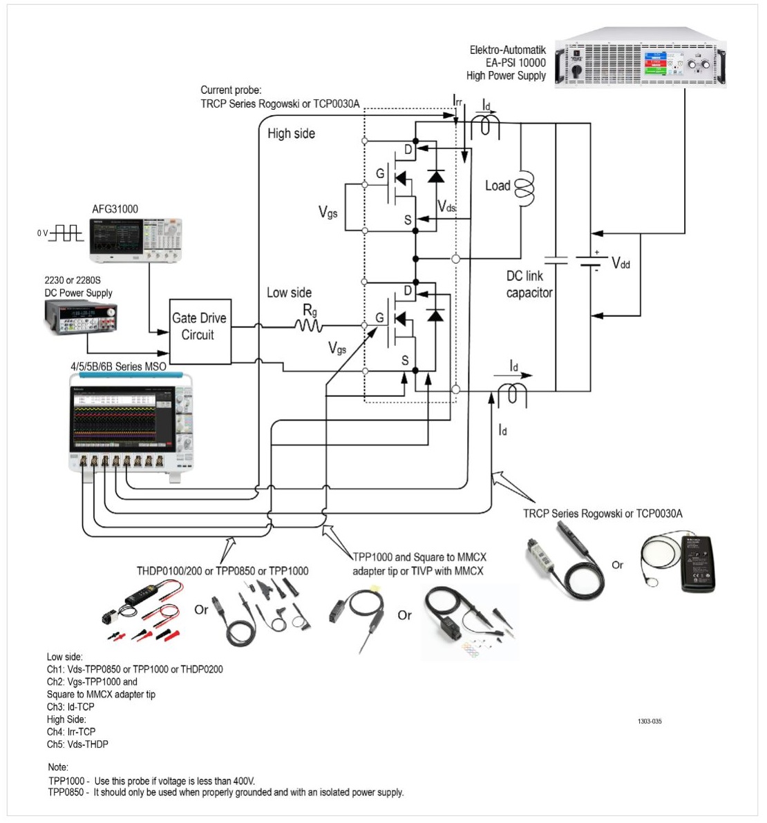
Figure 9 shows the equipment setup for running a Double Pulse Test. The following equipment is required:
- AFG31000: Connects to the isolated gate driver and uses the Double Pulse Test application on the unit to quickly generate the pulses with varying pulse widths. The isolated gate driver is what turns the MOSFET on.
- Oscilloscope: 4/5/6 Series MSO (this setup uses a Tektronix 5 Series MSO): Measures VDS, VGS, and ID.
- Double Pulse Test Software on the scope: Opt. WBGDPT on the 4/5/6 Series MSO to make automated measurements
- Probes for Double Pulse Test on the low side device and diode reverse recovery on the high side:
Low side probing:
- – Ch1: VDS - TPP Series or THDP/TMDP Series voltage probe
- – Ch2: VGS - TPP Series or TIVP Isolated probes with MMCX adapter tips.
- – Ch3: ID - TCP Series current probe
High side probing:
- – Ch4: IRR - TCP Series current probe
- – Ch5: VDS - THDP/TMDP Series voltage probe
- DC power supplies:
High voltage power supply:
- – EA-PSI 10000 programmable power supply up to 2 kV and 30 kW
- – 2657A High Voltage Source Meter Unit (SMU) up to 3 kV
- – 2260B-800-2, programmable DC power supply up to 800 V
Power supply to gate drive circuit:
- – Series 2230 or Series 2280S DC power supply
Double Pulse App on the AFG31000
The AFG31000 Double Pulse Test application can be downloaded directly from the tek.com website and installed onto the AFG31000. Figure 10 shows the icon of the Double Pulse Test on the home screen of the AFG31000 after the application is downloaded and installed on the unit.
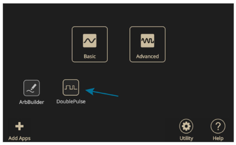
The Double Pulse Test application lets the user create pulses with varying pulse widths, which has been the main user pain point due to the time-consuming methods to create pulses with varying pulse widths. Some of these methods include creating waveforms on the PC and uploading them to the function generator. Others are using microcontrollers that require a lot of effort and time to program. The Double Pulse Test application on the AFG31000 enables this from the front display. The application is intuitive and quick to setup. The first pulse width is adjusted to get the desired switching current value. The second pulse could also be adjusted independently of the first pulse and is usually shorter than the first pulse so that the power device is not destroyed. The user also has the capability of defining the time gaps between each pulse.
Figure 11 shows the Double Pulse Test application window. Here the user can set the:
- Number of pulses: 2 to 30 pulses
- High and low voltage magnitude (V)
- Trigger delay (s)
- Trigger source – manual, external, or timer
- Load – 50 Ω or high Z
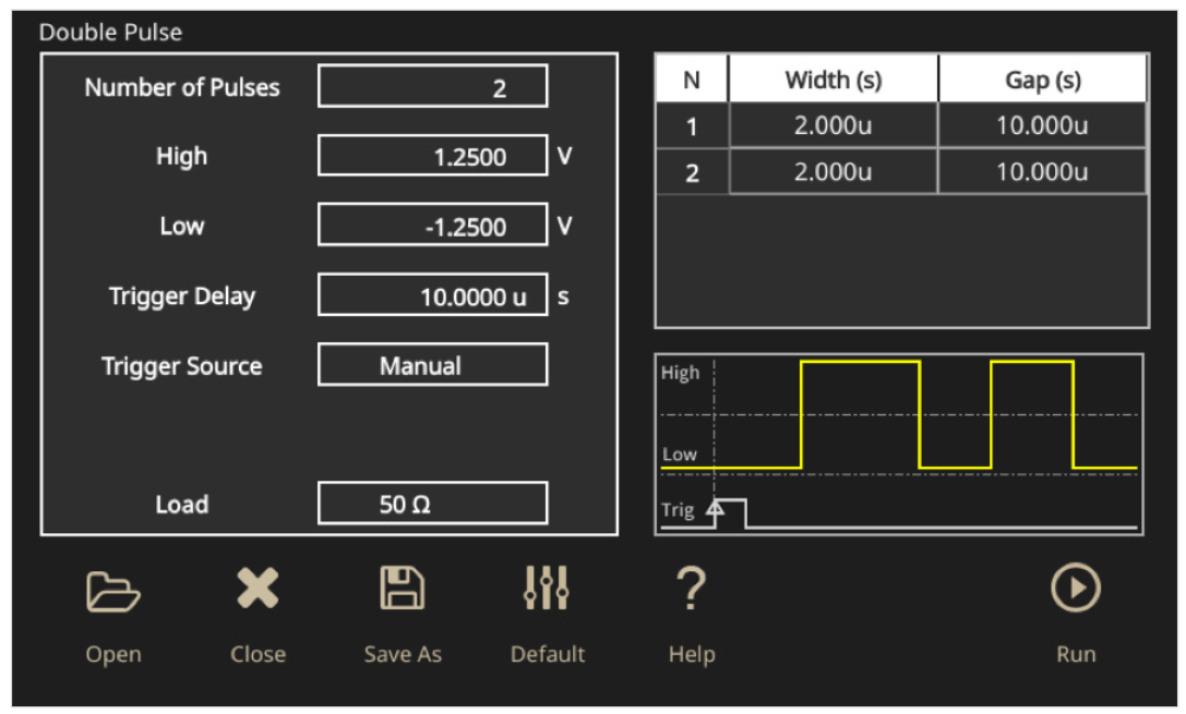
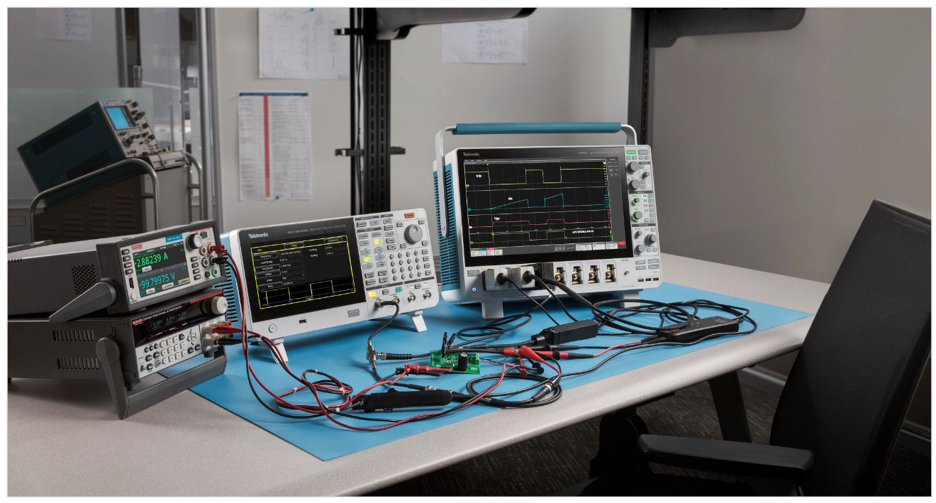
Figure 12 shows an actual test setup for the Double Pulse Test.
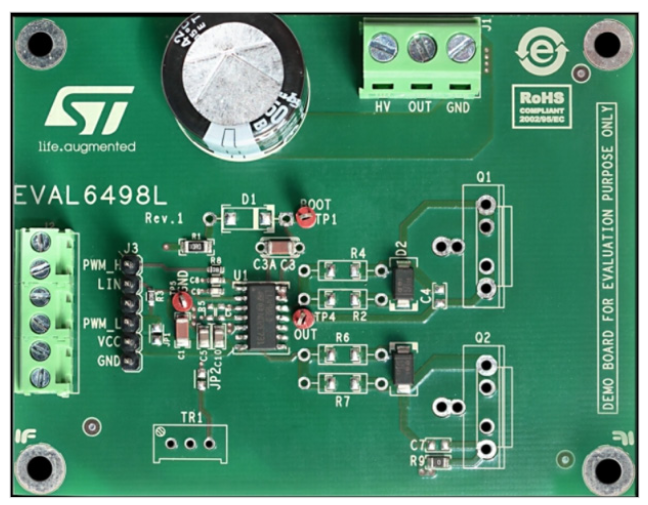
In this example, an ST Micro-Electronics evaluation board is being used as a gate driver for N-channel power MOSFETs and IGBTs: EVAL6498L shown in Figure 13.
The MOSFETs that were used are also from ST MicroElectronics: STFH10N60M2. These are N-channel 600V MOSFETs, rated at 7.5 A drain current.
Other equipment and devices used in the test circuit include:
- Tektronix 4, 5 or 6 Series MSO oscilloscope
- Tektronix current probe TCP0030A-120 MHz
- Tektronix high voltage differential probes: TMDP0200
- Keithley DC power supply – 2280S (supplies power to the gate driver IC)
- Keithley 2461 SMU Instrument (supplies voltage to the inductor)
- Inductor: ~1 mH
The power connections are as follows:
- The MOSFETs are soldered onto the board. Q2 is the low side, and Q1 is the high side.
- Gate and source on Q1 will need to be shorted since Q1 will not be turned on.
- Gate resistor is soldered for Q2. R = 100 Ω.
- CH1 from the AF31000 is connected to inputs PWM_L and GND on the eval board.
- Keithley power supply is connected to Vcc and GND inputs on the eval board to provide power to the gate driver IC.
- Keithley 2461 SMU Instrument is connected to HV and GND to provide power to the inductor.
- The inductor is then connected to HV and OUT
Double Pulse Test Measurements
Once all the power connections have been safely connected, we can connect the probes from the oscilloscope to Q2 (low side MOSFET) as shown in Figure 14.
- A passive probe is connected to VGS.
- Differential voltage probes are connected to VDS.
- TCP0030A current probe through a loop on the source lead of the MOSFET.
Careful probing and optimization will help the user get good results. There are steps that the user can take to make accurate and repeatable measurements like removing voltage, current and timing errors from the measurement. Automated measurement software such as the WBG-DPT option for the 4/5/6 Series MSOs eliminates manual steps to save time and provide repeatable results.
The Double Pulse Test can now be set on the AFG31000 as shown in the screen capture in Figure 15.
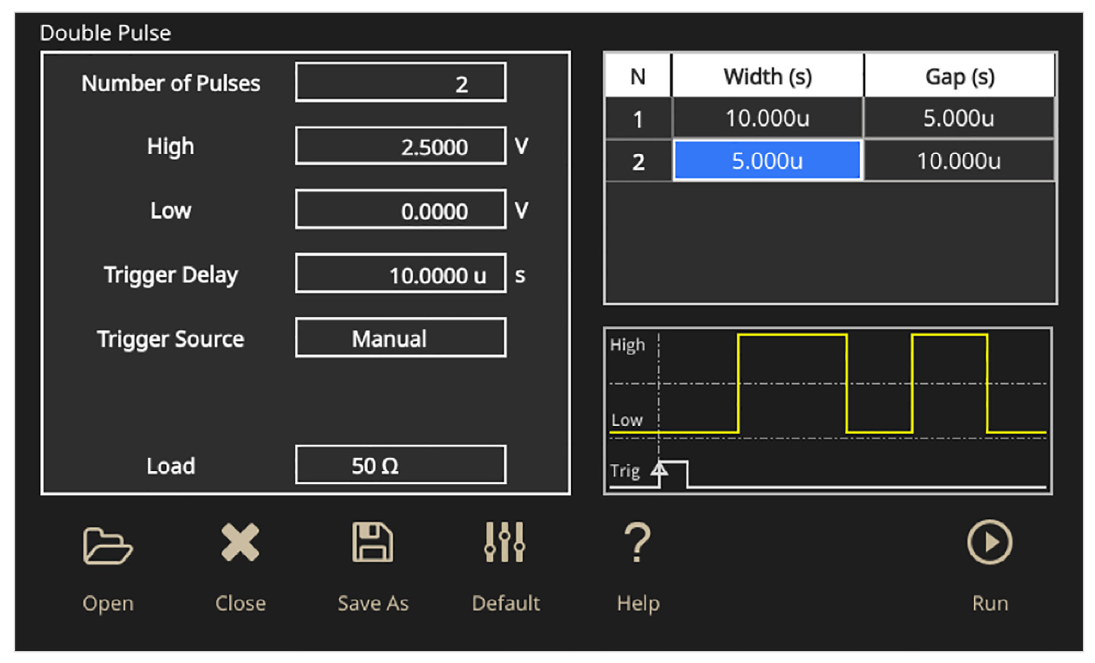
The amplitude of the pulses is set to 2.5 V. The pulse width for the first pulse is set to 10 µs, the gap is set to 5 µs and the second pulse is set to 5 µs. The trigger is set to manual.
The SMU instrument is set to source 100 V into HV. With the gate drive signal and power supplies configured, it is time to configure and perform double pulse tests using the WBG-DPT app on the oscilloscope.
Double Pulse Test Software on the 4/5/6 Series MSO
The WBG-DPT application offers several important advantages over manual testing:
- Shorter test times
- Enables repeatable measurements, even on signals with ringing
- Make measurements as per JEDEC/IEC standards or using custom parameters
- Preset feature to facilitate oscilloscope setup
- Easy navigation between pulses and annotation
- Summarize measurements in results tables
- Document results with reports, session files and waveforms
- Full programmatic interface enables automation
- Pass/Fail testing with configurable limits and actions to be taken on failures
For more information about WBG-DPT app, refer to the datasheet.
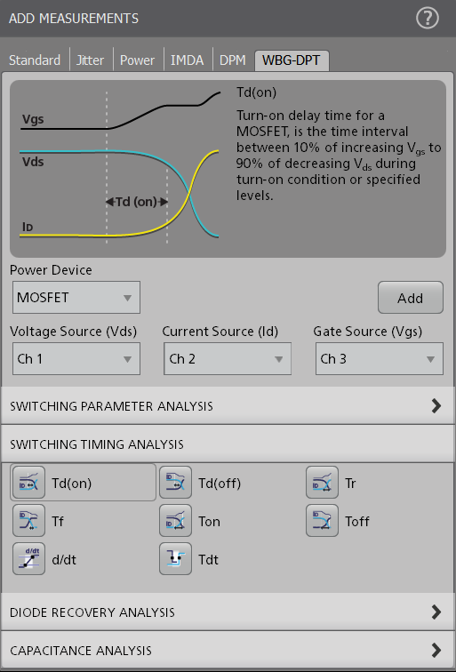
The measurements are categorized as Switching Parameter Analysis, Switching Timing Analysis and Diode Recovery Analysis.
WBG Deskew Function
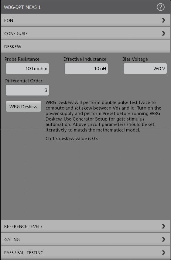
The WBG deskew function calculates the skew between Drain to Source Voltage (VDS) and Drain Current (ID) or Collector to Emitter Voltage (VCE) and Collector Current (IC) when the Power Device is a MOSFET or an IGBT respectively. The skew value is then applied on to the source to which VDS or VCE signal is configured on the scope.
WBG Deskew differs from conventional scope deskew.Conventionally, skew between probes is computed before starting any measurement on test setup. In WBG, the skew of the measurement system is performed as a postacquisition operation.
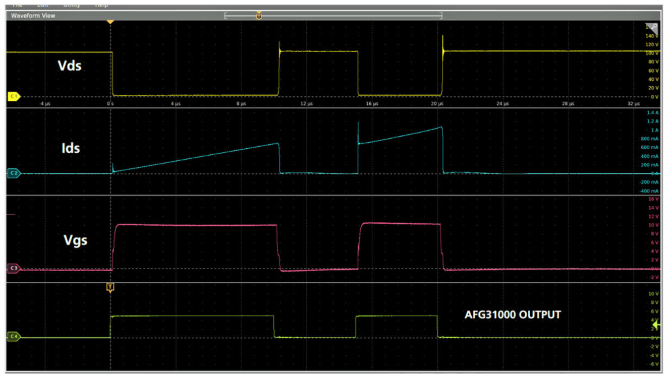
Notice the waveforms in Figure 18 resemble the ones shown in Figure 8. Again, the current overshoot seen on Ids is due to reverse recovery of the free-wheeling diode from the high side MOSFET/IGBT. This spike is intrinsic to the device being used and will contribute to the losses.
Measuring Turn-on and Turn-off Timing and Energy Losses
In order to calculate the turn-on and the turn-off parameters, we look at the falling edge of the first pulse and the rising edge of the second pulse.
The industry standard to measure the turn-on and turn-off parameters is shown in Figure 19.
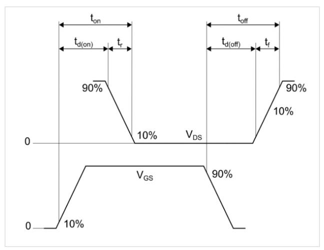
- td(on): Time interval between VGS at 10% of its peak and Vds at 90% of its peak amplitude.
- Tr: Time interval between VDS at 90% and 10% of its peak amplitude.
- td(off): Time interval between VGS at 90% of its peak and Vds at 10% of its peak amplitude.
- Tf: Time interval between VDS at 10% and 90% of its peak amplitude.
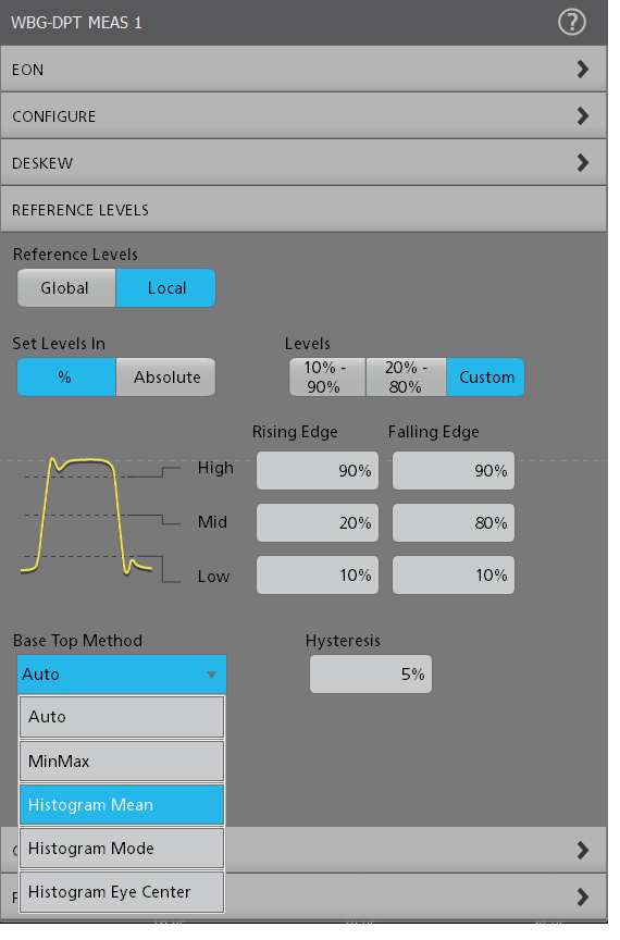
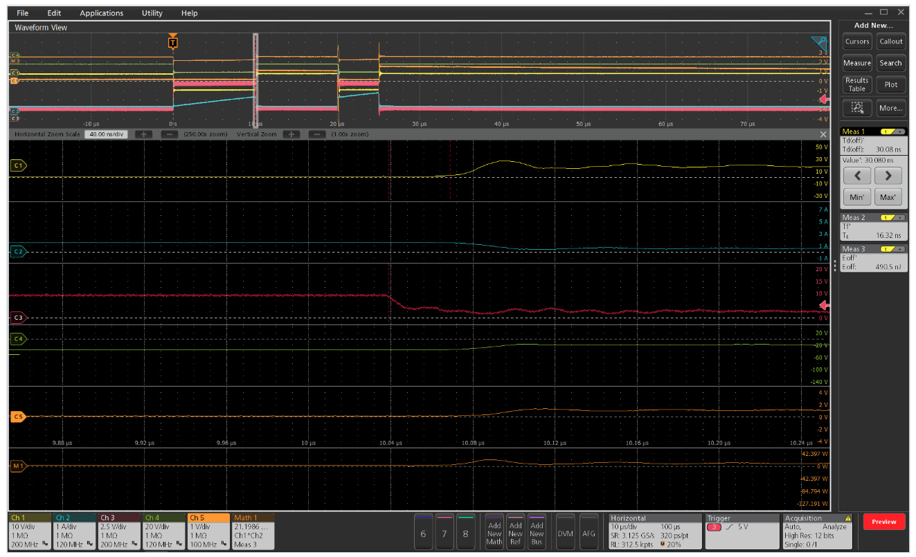
Figure 21 shows the waveforms captured on the scope and the measurements for turn-on parameters. On the oscilloscope, launch the WBG-DPT app. Select the ‘Power Device’ type as MOSFET. Configure the VDS, ID, and VGS sources.
Go to Switching Timing Analysis group. Add Td(on), Td(off), Tr, and Tf measurements.
Configure Td(on) measurement, click on Preset. This arms the scope for a single acquisition.
Turn on the Power supplies.
Turn on the AFG31000 to generate the output pulses.
The resulting waveforms are captured on the scope as shown in Figure 21.
The following equation is then used to calculate the energy losses during the transition:

Typically, designers would use the integral function on the oscilloscope for this specific energy loss computation. The WBG-DPT app offers the Eon measurement under the Switching Parameter Analysis group. This measurement sets up the integration and quickly displays the result.
The same equation from above can be used to calculate energy losses during the turn-off transition:

The DPT application includes an automatic Eoff measurement in the Switching Parameter Analysis menu.This performs the calculations and provides the energy loss results directly.
Note: The data shown in scope captures is for reference only.
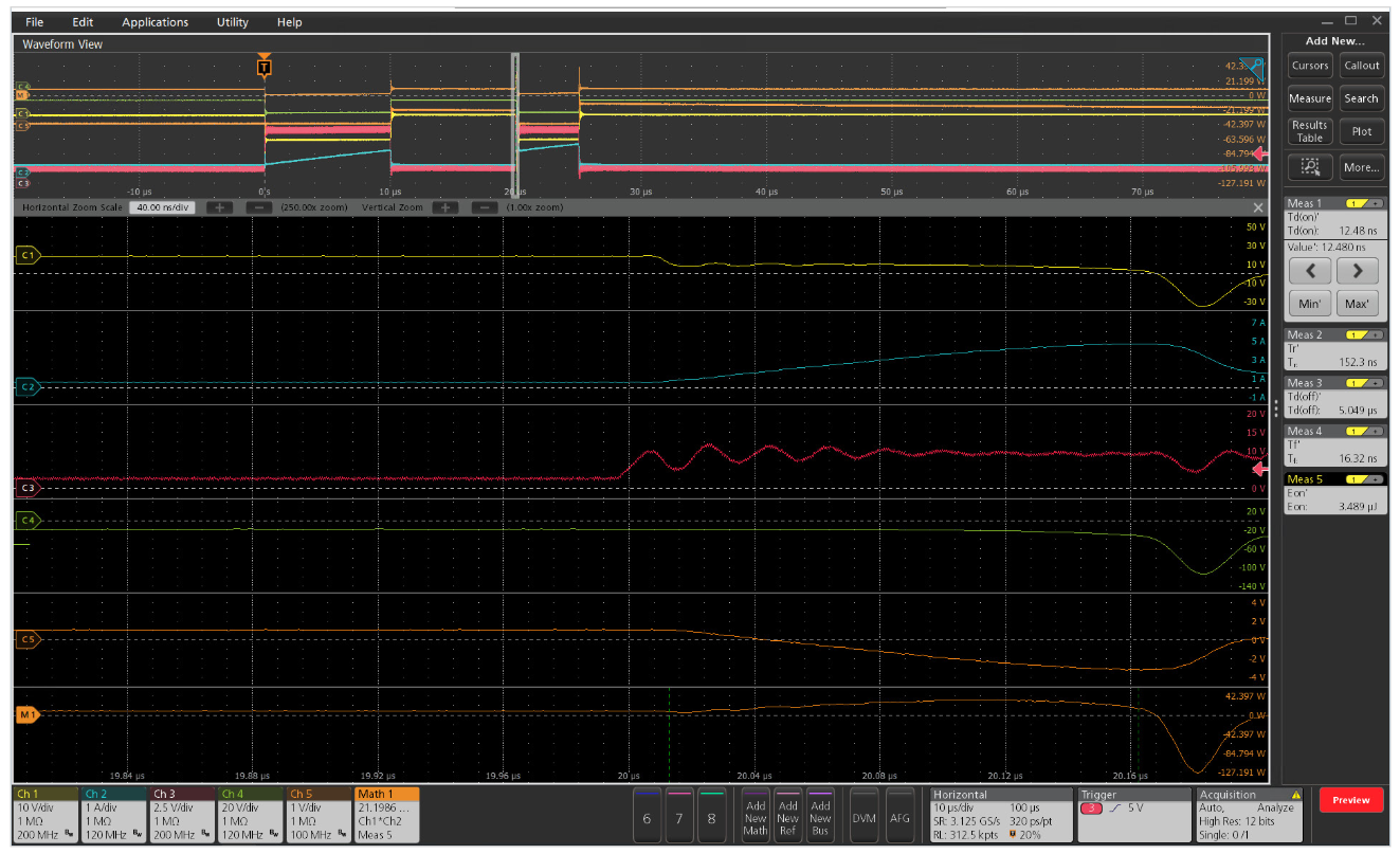
Figure 22 shows the turn-off waveforms measurements obtained using the scope cursors.
Measuring Reverse Recovery
Now, the reverse recovery characteristics of the MOSFET need to be measured.
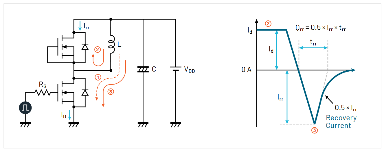
Reverse recovery current occurs during the turn-on of the second pulse. As shown in Figure 23, the diode is conducting in a forward condition during phase 2. As the low side MOSFET turns on again, the diode should immediately switch to a reverse blocking condition; however, the diode will conduct in a reverse condition for a short period of time, which is known as the reverse recovery current. This reverse recovery current is translated into energy losses, which directly impact the efficiency of the power converter. The measurements are now done on the high side MOSFET. Id is measured through the high side MOSFET and Vsd across the diode.
Figure 23 also shows how reverse recovery parameters are retrieved below.
Reverse Recovery Parameters: trr (reverse recovery time), Irr (reverse recovery current), Qrr (reverse recovery charge), Err (reverse recovery energy), di/dt, and Vsd (forward on voltage).
The following equation is then used to calculate the energy losses during the transition:

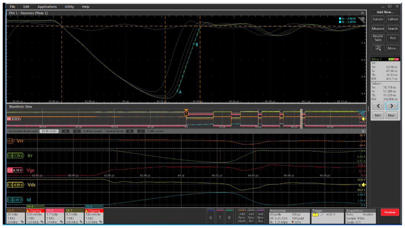
The WBG-DPT supports Trr , Qrr, and Err measurements under the Diode Reverse Recovery group. The waveforms and captured results are shown in Figure 24.
Multiple Trr measurements can also be displayed in an overlapped plot that shows selected pulse with annotation, tangent lines and configured values.
Measuring Deadtime
For switching devices in half-bridge configuration, one switch must be off before the other switch turns on in order to ensure the integrity of the DUT and safety of personnel. If both switches turn on at the same time, “shootthrough” occurs, which will cause failure. However, leaving both switches off for too long impacts efficiency. Thus, optimizing deadtime is a critical design goal.
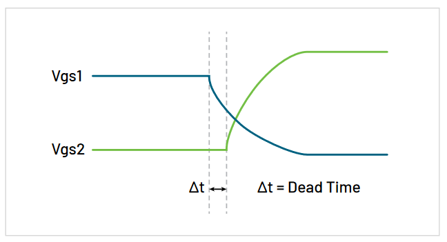
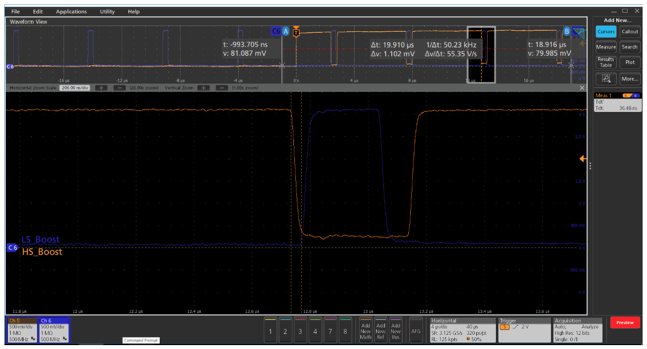
Deadtime (Tdt) is the time delay between the turn off time of one MOSFET and turn on time of the other MOSFET, measured on the gate drive signals for each MOSFET. Deadtime is shown as Δt in Figure 25.
The WBG-DPT application includes an automated deadtime measurement which can be found under the Switching Timing Analysis tab, as shown in Figure 16. The Tdt measurement is shown in Figure 26 in the badge on the right side of the display. The deadtime is the time interval between the configured falling edge level of one gate voltage and the configured rising edge level of the other gate voltage. The default rising and falling edge levels are 50%. The measurement annotations (dashed vertical lines) indicate the deadtime measurements on the gate drive signal.
In some scenarios, the deadtime measurement must be performed on waveforms with slow rise or fall times. In those cases, custom edge levels can be configured in measurement. Custom levels can be relative with respect to the high and low levels of the waveform, or absolute values.
Conclusion
Double Pulse Test is the preferred test method to measure the switching parameters and evaluate the dynamic behaviors of power devices. Test and design engineers that use this application are interested in understanding the switching, timing, and reverse recovery behaviors of the power devices. The test requires two voltage pulses with varying pulse widths, which is the main user pain point due to the time-consuming methods to create pulses with varying pulse widths. Some of these methods include creating waveforms on the PC and uploading them to the function generator. Others are using microcontrollers that require a lot of effort and time to program. This application note has shown that the Tektronix AFG31000 Arbitrary Function Generator offers a straight forward method to create pulses with varying pulse widths right on the front display. The Double Pulse Test application on the AFG31000 is quick to set up and to output pulses, thus allowing design and test engineers to focus on gathering data and designing more efficient converters.
The WBG-DPT double pulse application on the 4/5/6 Series MSO enables standard-specific tests to analyze power devices’ behavior while saving time compared to manual testing.
The application includes a preset feature to help capture the right waveform, detailed configuration options to test beyond the standards, enables signal conditioning feature for analyzing noisy waveforms, offers navigation and annotation feature, and offers detailed documentation to enable repeatable measurements.
Automated double pulse test setup and analysis on the AFG31000 and 4/5/6 Series MSO combine to greatly reduce test times and achieve faster time to market for next generation power converters.
References
- https://www.tek.com/document/technical-brief/evolving-materials-and-testing-emerginggenerations-power-electronics
- https://www.tek.com/document/application-note/measuring-power-supply-switching-loss-oscilloscope
- Infineon: Double Pulse Test for IGBT & FWD – Principle https://u.dianyuan.com/upload/space/2011/07/29/1311925659-501009.pdf
- https://training.ti.com/understanding-mosfetdatasheets-switching-parameters
- https://www.mouser.com/datasheet/2/389/stfh10n60m2-974335.pdf
- https://www.st.com/resource/en/data_brief/eval6498l.pdf
- https://www.tek.com/datasheet/advanced-powermeasurement-and-analysis
- https://www.tek.com/document/application-note/measuring-vgs-wide-bandgap-semiconductors


