Meeting the Growing Need for Bandwidth
The communications industry’s insatiable need for bandwidth, driven primarily by the exploding growth in the Internet, has led to the industry’s recent and significant deployment of 10-Gb/s systems in accordance with the STM-64/OC-192 standards for SDH and SONET. Tektronix developed the CSA8000 sampling oscilloscope to aid designers with physical-layer testing at these aggressive speeds. High-speed, low-noise, tunable sampling modules 80C02 and 80C04 make it the ideal tool to test these new 10-Gb/s transmitter devices and systems.
The CSA8000 delivers nearly 2-times improvement in both conversion gain and signal-to-noise ratio (SNR) with the unique architecture of its 80C02 and 80C04 sampling modules. These modules also enable tighter tolerances to the ideal ITU optical reference receiver (ORR) response. The result is better repeatability of measurement results, giving designers greater confidence in the quality of their measurements when creating 10-Gb/s transmitters and networks.
Communications Industry Turns to 10-Gb/s Systems
The growth of the Internet, as well as e-commerce, virtual private networks, IP telephony, and other data-centric applications, is prompting a demand for increased bandwidth that shows no signs of slowing down. To keep up, network providers are being forced to move quickly from 2.5-Gb/s to 10-Gb/s system deployment. As the component prices for this technology continue to decrease, and the reliability of 10-Gb/s technologies increases, this trend will only intensify.
Telephone deregulation has also helped to fuel the drive to 10-Gb/s systems. New service providers are creating networks to compete with established carriers. To ensure their investment will have plenty of headroom for future needs, they are installing the most bandwidth possible, currently 10 Gb/s. Even the incumbents are actively upgrading legacy fiber to include 10-Gb/s capabilities.
Until recently, when 10-Gb/s systems could finally be deployed cost-effectively and reliably, the required growth in bandwidth was provided by dense wavelength division multiplexing (DWDM). With this technology, multiple wavelengths of light are used to carry many signals on a single fiber strand. Up to 160 channels per fiber are now possible with this approach, with each wavelength carrying a 2.5-Gb/s base signal, resulting in enormous increases in effective bandwidth.
Despite the promise of dramatically increased network capacity, DWDM has some limitations. Its most significant drawback is very simple – each wavelength requires a separate receiver called line-terminating equipment (LTE). For example, with 40 wavelengths, 40 LTEs are needed per fiber. Numbers like these have been viable given the cost of DWDM equipment and the space available in telephone company central offices. But to achieve a 4-times improvement in network bandwidth for this particular example would require installing a total of 160 separate LTEs at 2.5 Gb/s. A more attractive alternative is to upgrade to 10 Gb/s with 40 wavelengths to achieve data bandwidths with the same network capacity that offer greater effectiveness.
The Design Challenges at 10-Gb/s Rates
Although the typical complications are to be expected when negotiating a 4- times increase in the data rate, moving from a 2.5-Gb/s to a 10-Gb/s system involves new factors that make the transition an especially difficult challenge. In the electrical domain, 10-GHz narrow-band microwave components have been around for some time, but only recently have semiconductor processes advanced to the point where digital circuits and very broad-band analog circuits are possible at 10 Gb/s. Even though these new processes support extremely fast active devices, interconnect parasitic elements have a more significant impact on the response than in the past.
In addition, the interconnect between components, even with "chip on board" or hybrid technology, can easily create long delays relative to the unit interval. This is especially true considering that a 50-picosecond (ps) microstrip line (1/2 the bit interval) is about 6 mm on aluminum. The bond wires used to get on and off the IC then add a relatively large impedance in series with the transmission line, making a poor match to the line. This distributed nature, combined with imperfect source and load matching, can create either large aberrations that are delayed from the data edge, or a resonance with ringing through the data interval. These types of effects can reduce margins or cause pattern dependence. Simulating the effect of parasitic elements on crosstalk, timing and pulse settling is possible, but requires a great deal of intuition from the designer as to what is important and how it should be modeled.
In the optical domain, optical amplifiers and DWDM have changed the way systems are deployed. Optical amplifiers are replacing regenerators wherever possible because a single amplifier can simultaneously amplify all of the wavelengths in a DWDM system. Unfortunately, without regeneration, the analog waveform, including any distortion from dispersion and noise, is amplified and sent along through the next fiber length. The result is an accumulation of these effects over the total span between regenerators. To avoid crosstalk in DWDM systems, it is necessary to include some dispersion in the path to minimize four-wave mixing. Very careful dispersion management is required to ensure that, in aggregate, the accumulated dispersion results in a reasonable eye shape at the end of the fiber.
All these effects make it essential that designers carefully measure waveform performance when debugging systems during design or when verifying conformance in manufacturing and during network commissioning. Bit error rate (BER) measurements remain the ultimate test. Eye diagram measurements, such as mask conformance, noise, jitter, extinction ratio, and Q-Factor, along with pulse measurements characterizing rise time and aberrations, provide a direct view of the time domain characteristics and offer valuable insight into the source of error and margin problems.
Measurement Issues
One of the key ways that transmitter designers solve physical-layer signal problems is by looking at analog waveforms. At STM-64/OC-192 rates, the only way to capture these waveforms is with a sampling oscilloscope. General purpose oscilloscopes simply lack enough bandwidth or sufficiently low jitter to properly measure a 10-Gb/s signal. Conversely, modern sampling oscilloscopes support optical inputs with reference receiver response to allow for standardized, controlled measurements of high-speed transmitters, making it easier to compare measurements from different instruments and ensure interoperability with other telecom equipment. Some designers and manufacturing test engineers also prefer looking at the unfiltered waveform to understand the total signal output, which the receiver must then be able to handle.
Pulse response fidelity in the measurement equipment is crucial. To achieve an extinction ratio of 12 dB, the combined response of the device-under-test and the oscilloscope must settle to better than 6 percent in less than 50 ps from the 50% crossing. Clearly, the measurement system must be better than this in order to be useful. At lower rates, ITU standards clearly define the specific reference receiver response. These standards specify the scalar frequency response as having a Bessel-Thompson shape that is near Gaussian, with the –3 dB electrical power response roll-off point at three-fourths the bit rate. This would result in a rise time of 0.467 UI, 0.84% overshoot which peaks near the center of the interval, and settling to 0.12% by the center of the next bit interval. Along with providing a definition of an ideal receiver, the ITU standards describe the acceptable deviation from that ideal. For STM-16/OC-48, the allowable deviation is ±0.5 dB from DC to three-fourths the bit rate, increasing linearly (on the dB scale) to ±3 dB at 1.5 times the bit rate.
For STM-64/OC-192, the ITU standards have not yet been finalized, though the proposed response extends the methods used at STM-16, specifying a similar fourth-order Bessel-Thompson response with a bandwidth of three-fourths the bit rate (7.46 GHz). The acceptable deviation, however, is increased to ±0.85 dB from DC to three-fourths the bit rate, increasing linearly to ±4 dB at 1.5 times the bit rate.
Minimizing noise in the sampling oscilloscope is essential. If the measurement is being made through a tap that only provides a small percentage of the available power or is at the end of a long fiber in order to view the impact of accumulated noise or dispersion, the signal level might be small relative to the oscilloscope noise. For instance, for a –10 dBm signal with an extinction ratio of 13 dB, the difference between the high and low level is about 180 µw. If the oscilloscope noise level is 8 µw root mean square (RMS) or approximately 64 µw peak-to-peak (p-p) (good for a sampling oscilloscope), then the eye opening will be reduced by 35 percent just from the oscilloscope noise. The resulting Q-factor would be 11:1. Noise also obscures the view of transient response variations in the signal caused by pattern dependence. The real cause of BER problems might be aberrations or crosstalk rather than random noise, but it goes unnoticed because of the measurement noise.
Limitations of the Traditional Sampling Architecture
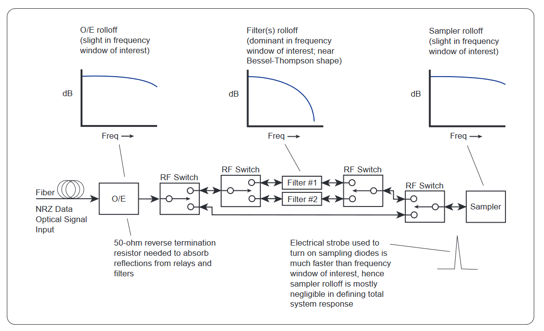
Traditionally, filtering for the reference receiver response within a sampling oscilloscope is provided by separate analog hardware filters inserted between the optical-to-electrical (O/E) converter and the sampler. Microwave switches are used to select between multiple filters and a full bandwidth path (see Figure 1). Although these filters provide an accurate roll-off to achieve the Bessel-Thompson response, they also introduce a finite impedance mismatch at their input and output. This mismatch at the filters reflects some of the input signal back to the O/E converter, which in turn reflects it back toward the sampler. The result is aberrations in the step response, indicated by ripple in the frequency response.
Similarly, imperfections in the switches, cables, and connectors cause reflections, further degrading the response. This threat to the response of the measurement system becomes especially acute when measuring higher data rate signals such as STM-64/OC-192 and 10-Gb/s waveforms. Reasons for this include the fact that component imperfections are worse at higher frequencies and that the unit interval (UI) is short relative to cabling delays. This means that aberrations are larger and can appear several periods later than where they were generated, possibly right in the center of the eye.
In order to minimize the effect of reflections, a reverse termination resistor is traditionally added at the O/E converter to absorb reflected signals. Unfortunately, the termination also absorbs half of the original output signal from the O/E converter, effectively increasing the noise floor of the instrument. Also, in previous lower data rate receivers, the reverse termination could be made nearly ideal over the relevant frequency range. This is much more difficult in a receiver for 10 Gb/s and the termination is typically less effective at absorbing reflections.
Tektronix’ 10-Gb/s Optical Module Solutions with the CSA8000
The new Tektronix 80C02 and 80C04 optical modules are optimized for physical-layer communications measurements at STM-64/OC-192. The 80C04 module is also capable of measuring 10.664-Gb/s signals (standard STM-64/OC-192 plus 7% forward error correction (FEC) as specified by ITU-T G.975). These modules deliver outstanding signal acquisition performance by implementing the reference receiver with an elegant, new approach that minimizes the number of components while staying within a tighter tolerance band than the previously proposed ITU standards. The result is breakthrough performance with exceptionally low noise and good fidelity at 10 Gb/s. This enables the CSA8000 with the 80C02 or 80C04 module to provide the best available signal acquisition performance for measuring STM-64/OC-192 waveforms.
Instead of employing the traditional filtering architecture, this new approach accomplishes the desired frequency roll-off by adjusting the bandwidth of the sampler low enough so that, without a filter, the system response falls within a tight tolerance band around the ideal Bessel-Thompson response. The 80C02 module provides an ORR response for STM-64/OC-192 and three higher bandwidth settings (12.5 GHz, 20 GHz, and 30 GHz). The 80C04 module delivers an ORR response for STM-64/OC-192, an ORR response for STM-64/OC-192 plus 7% FEC, and two higher bandwidth settings (20 GHz and 30 GHz). Because all these settings can also be achieved by simply adjusting the sampler bandwidth, the filter and microwave switch components can be eliminated (see Figure 2), resulting in a very clean transmission path between the O/E converter and the sampler. In fact, the cabling and termination in the sampler are good enough to eliminate the reverse termination in the O/E without causing excessive frequency response ripple. Elimination of the reverse termination in the O/E increases signal amplitude by about 3 dB, leading to a significantly better noise performance and more accurate measurements than were previously available in sampling oscilloscopes.
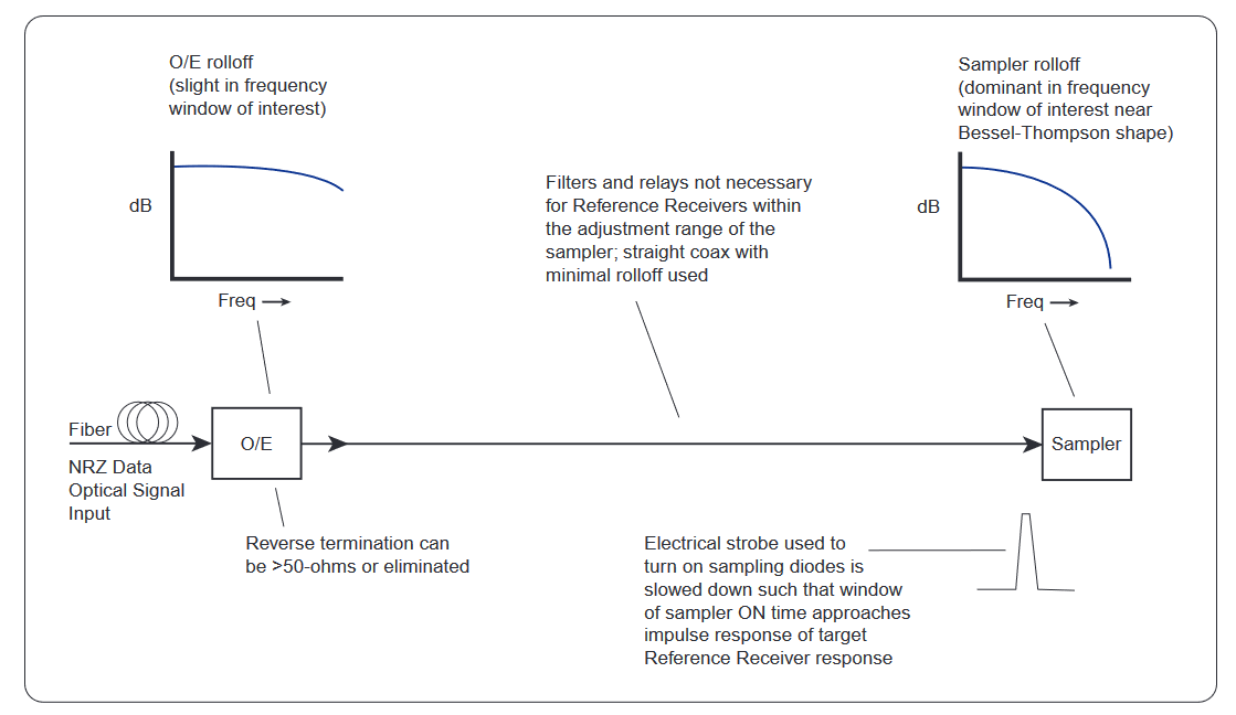
A more subtle consequence of removing the filter is that the reduced sampler bandwidth further improves noise performance. In a system with a filter, the sampler bandwidth must be tuned substantially higher to allow the combined system response to meet the specified bandwidth. Since the sampler is the dominant noise source, and its noise depends almost linearly on bandwidth, system performance is improved considerably by removing the filter and reducing sampler bandwidth.
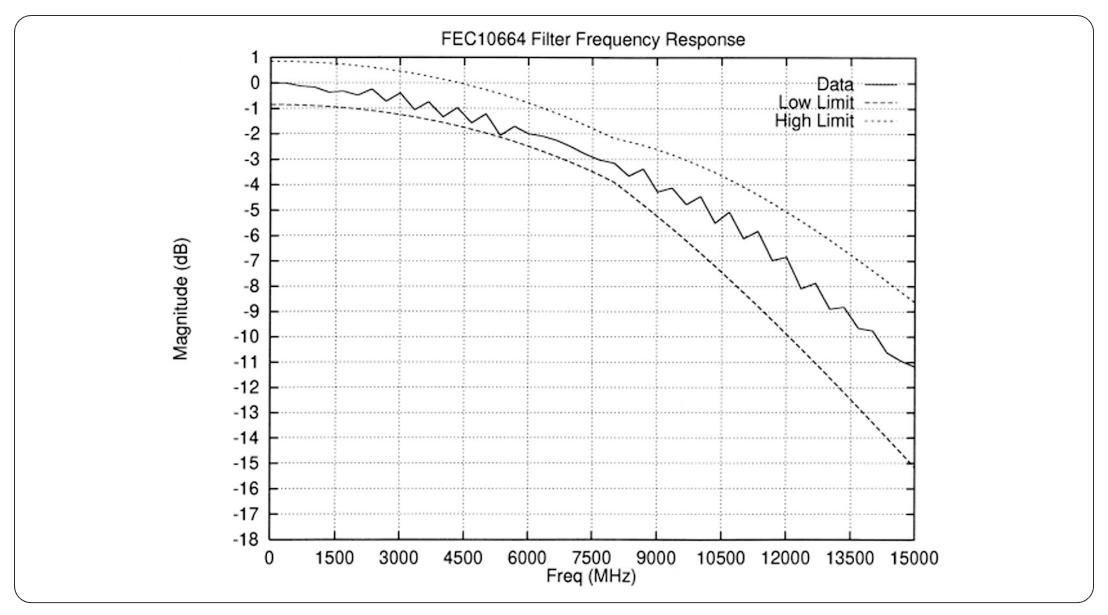
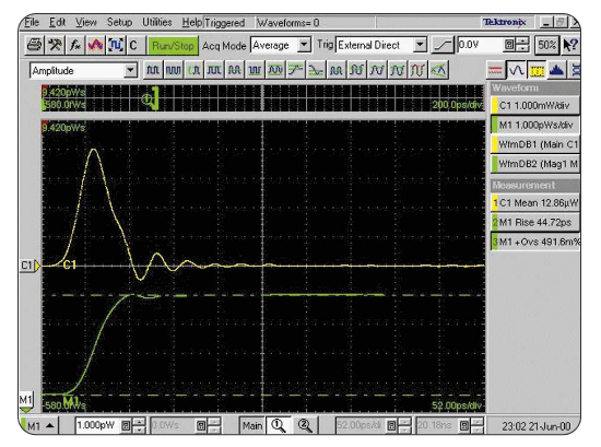
Figure 3 shows the measured 10.664 Gb/s reference receiver response of a typical 80C04 module along with the newly proposed tolerance curves for the ITU standard. Though this sampler filter has characteristics that deviate slightly from those of a Bessel-Thompson filter, it has properties that make it appropriate in this reference receiver application. Most importantly, the filter created by the sampler gating adds no overshoot or additional settling in the step response. In addition, the rise time is 44 ps, which is close to the ideal rise time of 46.9 ps. Figure 4 shows the measured impulse and computed step response of a typical 80C02 or 80C04 optical module.
This method of achieving a reference receiver system response also has the advantage of being tunable. This tunability enables the 80C04 module to support both the STM-64/OC-192 standard data rate of 9.953 Gb/s and the 7% FEC rate of 10.664 Gb/s. In addition, larger variations can be tolerated in O/E and interconnect components while still allowing tight correlation to the ideal ITU response standard. This new method directly supports an improved repeatability of accurate measurement results, creating a much higher level of confidence when evaluating 10-Gb/s devices.
The 80C01 module provides three reference receiver settings – STM-4/OC-12, STM-16/OC-48, and STM-64/OC-192. The two lower rates use separate filter components to produce the receiver response while the 10-Gb/s receiver is achieved using only sampler adjustments. In this case, the ability to adjust the sampler as a reference receiver provides coverage of the third rate. This would otherwise be impossible to fit into the module and would compromise the electrical performance at all of the rates given the extra switching required if a filter component were used.
CSA8000/80C02 or 80C04: The Best Waveform Measurement Solution for 10-Gb/s Devices
The Tektronix CSA8000, in combination with the 80C02 or 80C04 optical sampling module, is designed to satisfy the needs of the 10-Gb/s transmitter designer. Their unique reference receiver architecture makes them ideal for examining data signals at these aggressive speeds. By dramatically minimizing the number of components and employing a tunable response, the design of these modules enables tighter tolerances to the ideal ITU standards, while delivering a superior signal-to-noise ratio and an improved conversion gain for low-power signals. The result is a higher repeatability of measurement results, giving designers greater assurance of the quality of their measurements when creating 10-Gb/s components and networks. This is the type of optimal measurement performance designers need to confidently and efficiently produce solutions for the demanding STM-64/OC-192 standards.
Additional CSA8000 Features Further Boost Measurement Confidence
Along with the innovative 80C01, 80C02 and 80C04 sampling modules, the CSA8000 offers a host of other capabilities and features to ensure high-quality measurement of high-speed data signals.
The 80C03 datacom sampling module supports waveform compliance testing of Gigabit Ethernet and Fibre Channel. Its amplified optical-to-electrical (O/E) converter design enables the user to examine very low-level optical signals.
All four modules – the 80C01, 80C02, 80C03, and 80C04 – offer an optional clock recovery that aids in signal acquisition when a clock signal is not available, as is often the case. Triggering on a recovered clock filters out extremely long-term jitter, which is exactly how a receiver works. The eye diagram is, therefore, very representative of the operation of the receiver. Clock recovery eliminates the problems with triggering on the data and provides excellent trigger sensitivity due to the narrow loop bandwidth in the clock recovery phaselocked loop (PLL). Clock recovery also eliminates variable transmission delay effects when measuring the electrical signal at the end of a long fiber.
The CSA8000 itself delivers other features that help improve the repeatability of high-speed data measurements. When a signal amplitude is too low to measure, the CSA8000 can average and overlay multiple waveforms to create an eye diagram using FrameScan™ acquisition. This technique reduces the noise on the input signal, making it easier to observe the signal’s pulse shape as well as the effects of pattern-dependent (non-random) jitter.
FrameScan is unique in that it does not require a specialized bitpattern generator to create an averaged eye diagram. Instead, the pattern generator requires only a frame sync and possibly a 10-MHz frequency reference. A new ultra-stable horizontal timebase, which can be locked to an external frequency reference, allows the oscilloscope to look at edges far from the frame sync without adding excessive jitter – a capability not previously available in sampling oscilloscopes.
The CSA8000 also offers simultaneous electrical and optical inputs, which allow correction of board measurements with optical effects. This capability enables a designer to see how problems such as ground bounce, reflections between modules, and crosstalk affect the optical signal. Since these effects can cause noise, jitter, or pattern-dependent pulse distortion in the transmitter serializer/deserializer (SERDES), they can directly affect the analog waveform driving the laser or optical modulator. When problems in the optical signal are found, such as data-dependent jitter, the simultaneous display of electrical and optical signals can help the transmitter designer determine the cause of those problems. If there is a clear correlation between a transmitted waveform and other effects, such as ground bounce, the designer knows where to go to fix the problem.
Enabling a Brighter Optical Transport Network
CSA8000 Communications Signal Analyzer

Specifically designed for high-performance communications applications, the CSA8000 Communications Signal Analyzer is the ideal tool for design evaluation and manufacturing test of datacom and telecom components, transceiver subassemblies, and transmission systems.
Optical Sampling Modules
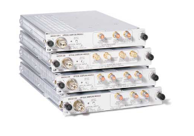
Equipped with one or more optical sampling modules, The CSA8000 sampling oscilloscopes provide complete optical test solutions for telecom (622 Mb/s to 10.664 Gb/s) or datacom (Fibre Channel and Gigabit Ethernet) applications, as well as general-purpose optical component testing. High-speed, low-noise, tunable sampling modules 80C02 and 80C04 make the CSA8000 the superior tool to test 10-Gb/s transmitter devices and systems.
Electrical Sampling Modules
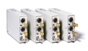
The 8000 Series sampling oscilloscopes, configured with one or more electrical sampling modules, provide complete electrical test solutions from 12.5 GHz to 50 GHz bandwidth, including a module for timedomain (TDR) characterization.
OTS9100 Optical Test System
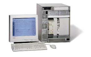
The OTS9100 Optical Test System consists of a 10 Gb/s SONET/SDH signal generator or transmitter and signal analyzer or receiver to help you focus on system transmission quality verification during production and installation.
For Further Information
Tektronix maintains a comprehensive, constantly expanding collection of application notes, technical briefs and other resources to help engineers working on the cutting edge of technology.
Please visit "Resources For You" at www.tektronix.com

